EP0892500A1 - System zur Auflösungserhöhung bei der Umwandlung von digitalen Daten in PWM-Signale zur Steuerung einer Vollbrückenausgangsstufe - Google Patents
System zur Auflösungserhöhung bei der Umwandlung von digitalen Daten in PWM-Signale zur Steuerung einer Vollbrückenausgangsstufe Download PDFInfo
- Publication number
- EP0892500A1 EP0892500A1 EP97830361A EP97830361A EP0892500A1 EP 0892500 A1 EP0892500 A1 EP 0892500A1 EP 97830361 A EP97830361 A EP 97830361A EP 97830361 A EP97830361 A EP 97830361A EP 0892500 A1 EP0892500 A1 EP 0892500A1
- Authority
- EP
- European Patent Office
- Prior art keywords
- bit
- bits
- input
- digital value
- datum
- Prior art date
- Legal status (The legal status is an assumption and is not a legal conclusion. Google has not performed a legal analysis and makes no representation as to the accuracy of the status listed.)
- Granted
Links
- 238000006243 chemical reaction Methods 0.000 claims abstract description 19
- 230000000295 complement effect Effects 0.000 claims description 6
- 238000000034 method Methods 0.000 claims description 6
- 230000001939 inductive effect Effects 0.000 claims 1
- 101001084254 Homo sapiens Peptidyl-tRNA hydrolase 2, mitochondrial Proteins 0.000 description 4
- 102100030867 Peptidyl-tRNA hydrolase 2, mitochondrial Human genes 0.000 description 4
- 238000010586 diagram Methods 0.000 description 2
- 230000010363 phase shift Effects 0.000 description 2
- 230000003190 augmentative effect Effects 0.000 description 1
- 230000006399 behavior Effects 0.000 description 1
- 230000000052 comparative effect Effects 0.000 description 1
- 230000006870 function Effects 0.000 description 1
- 238000000638 solvent extraction Methods 0.000 description 1
Images


Classifications
-
- H—ELECTRICITY
- H03—ELECTRONIC CIRCUITRY
- H03M—CODING; DECODING; CODE CONVERSION IN GENERAL
- H03M1/00—Analogue/digital conversion; Digital/analogue conversion
- H03M1/66—Digital/analogue converters
- H03M1/82—Digital/analogue converters with intermediate conversion to time interval
- H03M1/822—Digital/analogue converters with intermediate conversion to time interval using pulse width modulation
- H03M1/825—Digital/analogue converters with intermediate conversion to time interval using pulse width modulation by comparing the input signal with a digital ramp signal
-
- H—ELECTRICITY
- H02—GENERATION; CONVERSION OR DISTRIBUTION OF ELECTRIC POWER
- H02M—APPARATUS FOR CONVERSION BETWEEN AC AND AC, BETWEEN AC AND DC, OR BETWEEN DC AND DC, AND FOR USE WITH MAINS OR SIMILAR POWER SUPPLY SYSTEMS; CONVERSION OF DC OR AC INPUT POWER INTO SURGE OUTPUT POWER; CONTROL OR REGULATION THEREOF
- H02M7/00—Conversion of AC power input into DC power output; Conversion of DC power input into AC power output
- H02M7/42—Conversion of DC power input into AC power output without possibility of reversal
- H02M7/44—Conversion of DC power input into AC power output without possibility of reversal by static converters
- H02M7/48—Conversion of DC power input into AC power output without possibility of reversal by static converters using discharge tubes with control electrode or semiconductor devices with control electrode
- H02M7/53—Conversion of DC power input into AC power output without possibility of reversal by static converters using discharge tubes with control electrode or semiconductor devices with control electrode using devices of a triode or transistor type requiring continuous application of a control signal
- H02M7/537—Conversion of DC power input into AC power output without possibility of reversal by static converters using discharge tubes with control electrode or semiconductor devices with control electrode using devices of a triode or transistor type requiring continuous application of a control signal using semiconductor devices only, e.g. single switched pulse inverters
- H02M7/5387—Conversion of DC power input into AC power output without possibility of reversal by static converters using discharge tubes with control electrode or semiconductor devices with control electrode using devices of a triode or transistor type requiring continuous application of a control signal using semiconductor devices only, e.g. single switched pulse inverters in a bridge configuration
- H02M7/53871—Conversion of DC power input into AC power output without possibility of reversal by static converters using discharge tubes with control electrode or semiconductor devices with control electrode using devices of a triode or transistor type requiring continuous application of a control signal using semiconductor devices only, e.g. single switched pulse inverters in a bridge configuration with automatic control of output voltage or current
- H02M7/53873—Conversion of DC power input into AC power output without possibility of reversal by static converters using discharge tubes with control electrode or semiconductor devices with control electrode using devices of a triode or transistor type requiring continuous application of a control signal using semiconductor devices only, e.g. single switched pulse inverters in a bridge configuration with automatic control of output voltage or current with digital control
Definitions
- the present invention relates to techniques for driving a generic R-L actuator through an output power stage having a so-called bridge configuration and more in particular to a technique for driving an output bridge stage in a PWM mode thus partitioning the voltage delivered to the actuator and thereby controlling the current flowing through it.
- the control signal of the PWM driving system may, according to recently developed techniques, be generated by a circuit that transforms a predefined N-bit digital value permanently stored in a nonvolatile memory that can be scanned at a variable clock speed, in a digital signal whose amplitude is compatible with the input requisites of the output power stage, the duty-cycle of which is proportional to the N-bit digital value read from the memory.
- the comparator COMP generates a clock impulse for the toggle bistable circuit FF2 each time the CNT counter state equals the value of the sample to be converted.
- the unitary increment (highlighted in an exaggerated manner in Fig. 2) of the input sample value to be converted results in a double and symmetric decrement of the output duty-cycle.
- the unitary increment (highlighted in an exaggerated manner in Fig. 2) of the input sample value to be converted results in a double and symmetric decrement of the output duty-cycle.
- going from a sample value 188 to a sample value 189 results in a duty-cycle decrement as depicted by the dashed line of Fig. 2.
- a double duty-cycle differential increment is produced if compared to the case of a half-bridge output stage.
- the system of the present invention avoids such augmented duty-cycle increments for unitary variations of the value of input samples in driving a full-bridge.
- An object of the present patent application is a circuit that improves the definition of the above mentioned conversion process by increasing from N to N+2 bits the dimension of the input datum, thereby improving the control of the current in the actuator without incrementing the size (number of bits) of the digital comparator.
- the two signals IN1 and IN2 are obtained by converting into two PWM signals an original digital datum DATAIN which is considered stored in N+2 bits.
- the N msb of DATAIN will be referred to as VAL whereas the complementary of VAL, in respect to 2 N /2 , will be referred to as *VAL+1.
- the condition of null current through the load is obtained when the two input signals IN1 and IN2 are perfectly in phase with each other and with a duty-cycle equal to 50%.
- VAL a unitary increment of VAL corresponds a unitary decrement of *VAL+1 in order to maintain symmetry about the value corresponding to a null current through the load (2 N /2 for the case of a generic N value).
- the value VAL is incremented from 145 to 146 and, correspondingly, the value of *VAL+1, symmetric about the value 128, is decremented from 111 to 110.
- the differential duty-cycle DIFF is therefore incremented by A+B+C+D pursuant a unitary increment/decrement of VAL and *VAL+1.
- the system permits to have a definition of 1/255 ((1/2 N ) in the case of a generic N value) for a differential duty-cycle ranging from 0 to 100%.
- the system of the present invention permits to obtain a greater definition without increasing the number of bits of the up/down counter (comparator).
- N is the number of bits of the up/down counter
- the system herein disclosed allows for the conversion of an input datum (original datum) mapped on N+2 bits.
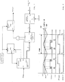
- Fig. 5 shows a block diagram of the system of the invention.
- the DATAIN value to be converted is mapped on N+2 bits in the memory. Among these, the N msb are indicated with VAL.
- the complementary value *VAL is obtained and the two digital values are loaded in two registers of N-bits each.
- the two lsb of the input value, together with the up/down signal of the counter, are used by the multiplexing block to select the datum to be compared.
- the two least significative bits of the input datum are used by a digital circuit to identify three intermediate levels between two consecutive values representable by an N-bit dynamic.
- the two supplementary lsb are used by a dedicated digital circuit to decide of "how much" the base duty-cycle (identified by DC145 and corresponding to the two lsb equal to zero) should be incremented or decremented.
- the system functions in a dynamic manner generating a different duty-cycle depending on the value of the two lsb of the datum to be converted and of the counting direction of the up/down counter.
- the comparator thereby generates the two IN1 and IN2 signals that drive the output power stage.
- DATO1 is always equal to VAL+1.
Landscapes
- Engineering & Computer Science (AREA)
- Theoretical Computer Science (AREA)
- Power Engineering (AREA)
- Analogue/Digital Conversion (AREA)
- Control Of Motors That Do Not Use Commutators (AREA)
- Control Of Direct Current Motors (AREA)
- Inverter Devices (AREA)
Priority Applications (4)
| Application Number | Priority Date | Filing Date | Title |
|---|---|---|---|
| EP97830361A EP0892500B1 (de) | 1997-07-17 | 1997-07-17 | System zur Auflösungserhöhung bei der Umwandlung von digitalen Daten in PWM-Signale zur Steuerung einer Vollbrückenausgangsstufe |
| DE69719317T DE69719317D1 (de) | 1997-07-17 | 1997-07-17 | System zur Auflösungserhöhung bei der Umwandlung von digitalen Daten in PWM-Signale zur Steuerung einer Vollbrückenausgangsstufe |
| US09/112,999 US6310912B1 (en) | 1997-07-17 | 1998-07-10 | System for increasing the definition in converting a digital datum in a PWM signal for driving a full-bridge output stage |
| JP20384998A JP4187831B2 (ja) | 1997-07-17 | 1998-07-17 | デジタルデータをフルブリッジ出力段部駆動用のpwm信号に変換するときの精細度を増加させる装置及び方法 |
Applications Claiming Priority (1)
| Application Number | Priority Date | Filing Date | Title |
|---|---|---|---|
| EP97830361A EP0892500B1 (de) | 1997-07-17 | 1997-07-17 | System zur Auflösungserhöhung bei der Umwandlung von digitalen Daten in PWM-Signale zur Steuerung einer Vollbrückenausgangsstufe |
Publications (2)
| Publication Number | Publication Date |
|---|---|
| EP0892500A1 true EP0892500A1 (de) | 1999-01-20 |
| EP0892500B1 EP0892500B1 (de) | 2003-02-26 |
Family
ID=8230711
Family Applications (1)
| Application Number | Title | Priority Date | Filing Date |
|---|---|---|---|
| EP97830361A Expired - Lifetime EP0892500B1 (de) | 1997-07-17 | 1997-07-17 | System zur Auflösungserhöhung bei der Umwandlung von digitalen Daten in PWM-Signale zur Steuerung einer Vollbrückenausgangsstufe |
Country Status (4)
| Country | Link |
|---|---|
| US (1) | US6310912B1 (de) |
| EP (1) | EP0892500B1 (de) |
| JP (1) | JP4187831B2 (de) |
| DE (1) | DE69719317D1 (de) |
Cited By (4)
| Publication number | Priority date | Publication date | Assignee | Title |
|---|---|---|---|---|
| EP1137162A1 (de) * | 2000-03-23 | 2001-09-26 | STMicroelectronics S.r.l. | Analogdigitale Pulsbreitenmodulatorsteuerschaltung |
| WO2002035893A1 (en) * | 2000-10-25 | 2002-05-02 | Koninklijke Philips Electronics N.V. | Circuit arrangement |
| EP1014552B1 (de) * | 1998-12-23 | 2003-04-23 | STMicroelectronics S.r.l. | Umwandlung von einem numerischen Befehlswert in ein Pulsbreitenmodulationsantriebsignal mit konstanter Frequenz für eine elektromagnetische Last |
| ITUB20153268A1 (it) * | 2015-08-27 | 2017-02-27 | St Microelectronics Srl | Unita' di controllo per un circuito a ponte, e relativo procedimento e circuito integrato |
Families Citing this family (18)
| Publication number | Priority date | Publication date | Assignee | Title |
|---|---|---|---|---|
| US6519168B2 (en) * | 2000-07-24 | 2003-02-11 | Chippower.Com, Inc. | High frequency DC to AC inverter |
| CA2483672A1 (en) * | 2002-06-19 | 2003-12-31 | Wavecrest Laboratories Llc | Adaptive control architecture for electric machines |
| JP2006238698A (ja) * | 2002-06-19 | 2006-09-07 | Wavecrest Lab Llc | 向上した性能及び効率を備える適応電気モータ及び発電機 |
| US7886164B1 (en) | 2002-11-14 | 2011-02-08 | Nvidia Corporation | Processor temperature adjustment system and method |
| US7882369B1 (en) | 2002-11-14 | 2011-02-01 | Nvidia Corporation | Processor performance adjustment system and method |
| US7849332B1 (en) | 2002-11-14 | 2010-12-07 | Nvidia Corporation | Processor voltage adjustment system and method |
| US7479753B1 (en) * | 2004-02-24 | 2009-01-20 | Nvidia Corporation | Fan speed controller |
| US7376182B2 (en) * | 2004-08-23 | 2008-05-20 | Microchip Technology Incorporated | Digital processor with pulse width modulation module having dynamically adjustable phase offset capability, high speed operation and simultaneous update of multiple pulse width modulation duty cycle registers |
| JP4837354B2 (ja) * | 2005-09-30 | 2011-12-14 | ルネサスエレクトロニクス株式会社 | Pwm信号生成装置及びpwm信号生成方法並びにモータ制御装置及びモータ制御方法 |
| US9134782B2 (en) | 2007-05-07 | 2015-09-15 | Nvidia Corporation | Maintaining optimum voltage supply to match performance of an integrated circuit |
| JP2008283782A (ja) * | 2007-05-10 | 2008-11-20 | Mitsuba Corp | モータ駆動装置 |
| US8370663B2 (en) | 2008-02-11 | 2013-02-05 | Nvidia Corporation | Power management with dynamic frequency adjustments |
| JP2010115066A (ja) * | 2008-11-08 | 2010-05-20 | Asahi Kasei Toko Power Device Corp | Pwm制御回路 |
| US9256265B2 (en) | 2009-12-30 | 2016-02-09 | Nvidia Corporation | Method and system for artificially and dynamically limiting the framerate of a graphics processing unit |
| US9830889B2 (en) | 2009-12-31 | 2017-11-28 | Nvidia Corporation | Methods and system for artifically and dynamically limiting the display resolution of an application |
| US8839006B2 (en) | 2010-05-28 | 2014-09-16 | Nvidia Corporation | Power consumption reduction systems and methods |
| KR20140057877A (ko) * | 2012-11-05 | 2014-05-14 | 콘티넨탈 오토모티브 시스템 주식회사 | H-브릿지 회로 제어시스템 및 그 제어방법 |
| EP4102703A1 (de) * | 2021-06-09 | 2022-12-14 | Delta Electronics (Thailand) Public Co., Ltd. | Alternierende asymmetrische phasenverschiebungsmodulation |
Citations (3)
| Publication number | Priority date | Publication date | Assignee | Title |
|---|---|---|---|---|
| US4590457A (en) * | 1983-12-20 | 1986-05-20 | American Microsystems, Inc. | Digital to analog converter utilizing pulse width modulation |
| US5103462A (en) * | 1989-10-06 | 1992-04-07 | Endress U. Hauser Gmbh U. Co. | Arrangement for the conversion of an electrical input quantity into a dc signal proportional thereto |
| EP0760552A1 (de) * | 1995-08-31 | 1997-03-05 | STMicroelectronics S.r.l. | Verfahren und Schaltung zur pulsbreitenmodulierten Brückensteuerung und Plattenantrieb unter Verwendung derselben |
Family Cites Families (4)
| Publication number | Priority date | Publication date | Assignee | Title |
|---|---|---|---|---|
| US4138632A (en) * | 1977-04-04 | 1979-02-06 | Pneumo Corporation | Pulse width modulator digital servo system |
| US4894598A (en) * | 1986-11-20 | 1990-01-16 | Staubli International Ag | Digital robot control having an improved pulse width modulator |
| DE69034055D1 (de) * | 1989-10-02 | 2003-05-08 | Canon Kk | Bilderzeugungsgerät und Modulationsverfahren |
| JP3687861B2 (ja) * | 1995-03-20 | 2005-08-24 | 株式会社ルネサステクノロジ | 制御システム及び相補ノンオーバーラップpwm信号を形成する方法 |
-
1997
- 1997-07-17 EP EP97830361A patent/EP0892500B1/de not_active Expired - Lifetime
- 1997-07-17 DE DE69719317T patent/DE69719317D1/de not_active Expired - Lifetime
-
1998
- 1998-07-10 US US09/112,999 patent/US6310912B1/en not_active Expired - Lifetime
- 1998-07-17 JP JP20384998A patent/JP4187831B2/ja not_active Expired - Fee Related
Patent Citations (3)
| Publication number | Priority date | Publication date | Assignee | Title |
|---|---|---|---|---|
| US4590457A (en) * | 1983-12-20 | 1986-05-20 | American Microsystems, Inc. | Digital to analog converter utilizing pulse width modulation |
| US5103462A (en) * | 1989-10-06 | 1992-04-07 | Endress U. Hauser Gmbh U. Co. | Arrangement for the conversion of an electrical input quantity into a dc signal proportional thereto |
| EP0760552A1 (de) * | 1995-08-31 | 1997-03-05 | STMicroelectronics S.r.l. | Verfahren und Schaltung zur pulsbreitenmodulierten Brückensteuerung und Plattenantrieb unter Verwendung derselben |
Cited By (8)
| Publication number | Priority date | Publication date | Assignee | Title |
|---|---|---|---|---|
| EP1014552B1 (de) * | 1998-12-23 | 2003-04-23 | STMicroelectronics S.r.l. | Umwandlung von einem numerischen Befehlswert in ein Pulsbreitenmodulationsantriebsignal mit konstanter Frequenz für eine elektromagnetische Last |
| US6594308B1 (en) | 1998-12-23 | 2003-07-15 | Stmicroelectronics S.R.L. | Conversion of a numeric command value in a constant frequency PWM drive signal for an electromagnetic load |
| EP1137162A1 (de) * | 2000-03-23 | 2001-09-26 | STMicroelectronics S.r.l. | Analogdigitale Pulsbreitenmodulatorsteuerschaltung |
| US6385067B2 (en) | 2000-03-23 | 2002-05-07 | Stmicroelectronics S.R.L. | Analog/digital PWM control circuit of a winding |
| WO2002035893A1 (en) * | 2000-10-25 | 2002-05-02 | Koninklijke Philips Electronics N.V. | Circuit arrangement |
| CN100393180C (zh) * | 2000-10-25 | 2008-06-04 | 皇家菲利浦电子有限公司 | 电路装置 |
| ITUB20153268A1 (it) * | 2015-08-27 | 2017-02-27 | St Microelectronics Srl | Unita' di controllo per un circuito a ponte, e relativo procedimento e circuito integrato |
| US9780770B2 (en) | 2015-08-27 | 2017-10-03 | Stmicroelectronics S.R.L. | Control unit for a bridge circuit, and related method and integrated circuit |
Also Published As
| Publication number | Publication date |
|---|---|
| EP0892500B1 (de) | 2003-02-26 |
| US6310912B1 (en) | 2001-10-30 |
| JPH11103586A (ja) | 1999-04-13 |
| DE69719317D1 (de) | 2003-04-03 |
| JP4187831B2 (ja) | 2008-11-26 |
Similar Documents
| Publication | Publication Date | Title |
|---|---|---|
| EP0892500B1 (de) | System zur Auflösungserhöhung bei der Umwandlung von digitalen Daten in PWM-Signale zur Steuerung einer Vollbrückenausgangsstufe | |
| US5337338A (en) | Pulse density modulation circuit (parallel to serial) comparing in a nonsequential bit order | |
| US5028926A (en) | Successive type analog-to-digital converter with a variable reference voltage for the digital to analog converter | |
| US5638017A (en) | Pulse width modulation circuit | |
| EP1014552B1 (de) | Umwandlung von einem numerischen Befehlswert in ein Pulsbreitenmodulationsantriebsignal mit konstanter Frequenz für eine elektromagnetische Last | |
| US20020041246A1 (en) | Device and control structure of multi-level pulse width modulation | |
| EP0586228B1 (de) | Schaltung zur Berechnung des Gleichstromwertes in einem digitalen Aufzeichnungs-/Wiedergabesystem | |
| US5155488A (en) | D/a conversion circuit | |
| US6310913B1 (en) | Circuit and method for modulating pulse width | |
| US7028108B2 (en) | System and method for controlling data transfer for data array control unit having first and second selector with data shift register | |
| US20010028319A1 (en) | Apparatus for and method of converting sampling frequency of digital signals | |
| EP0582311A2 (de) | Parallel-Serien-Umsetzer | |
| JPH05276036A (ja) | A/dコンバータのオフセット補償回路 | |
| US5479158A (en) | Priority selection circuit with increasing priority levels for non-selected requested devices | |
| EP0613289A1 (de) | Bildleser | |
| US6642875B2 (en) | PWM converting circuit, D/A converter and PWM converting method with improved resolution | |
| US5333263A (en) | Digital image processing apparatus | |
| KR100629538B1 (ko) | 제 1 디지털 신호의 에지와 제 2 디지털 신호의 에지 사이의 시간차를 검출하는 회로 | |
| EP0460775A2 (de) | Schaltung zur Erzeugung eines pulsförmigen Ausgangssignales aus drei binären Eingangssignalen | |
| EP1098507A2 (de) | Bildverarbeitungsvorrichtung | |
| KR0185924B1 (ko) | 디지탈데이타 검출장치 | |
| JPH0376311A (ja) | パルス幅変調回路 | |
| JPH06224708A (ja) | パルス幅変調回路 | |
| US5307474A (en) | Apparatus and method for processing literal operand computer instructions | |
| KR100258862B1 (ko) | 감마보상회로 |
Legal Events
| Date | Code | Title | Description |
|---|---|---|---|
| PUAI | Public reference made under article 153(3) epc to a published international application that has entered the european phase |
Free format text: ORIGINAL CODE: 0009012 |
|
| AK | Designated contracting states |
Kind code of ref document: A1 Designated state(s): DE FR GB IT |
|
| AX | Request for extension of the european patent |
Free format text: AL;LT;LV;RO;SI |
|
| 17P | Request for examination filed |
Effective date: 19990527 |
|
| AKX | Designation fees paid |
Free format text: DE FR GB IT |
|
| GRAH | Despatch of communication of intention to grant a patent |
Free format text: ORIGINAL CODE: EPIDOS IGRA |
|
| GRAH | Despatch of communication of intention to grant a patent |
Free format text: ORIGINAL CODE: EPIDOS IGRA |
|
| GRAA | (expected) grant |
Free format text: ORIGINAL CODE: 0009210 |
|
| AK | Designated contracting states |
Designated state(s): DE FR GB IT |
|
| REG | Reference to a national code |
Ref country code: GB Ref legal event code: FG4D |
|
| REF | Corresponds to: |
Ref document number: 69719317 Country of ref document: DE Date of ref document: 20030403 Kind code of ref document: P |
|
| PG25 | Lapsed in a contracting state [announced via postgrant information from national office to epo] |
Ref country code: DE Free format text: LAPSE BECAUSE OF FAILURE TO SUBMIT A TRANSLATION OF THE DESCRIPTION OR TO PAY THE FEE WITHIN THE PRESCRIBED TIME-LIMIT Effective date: 20030527 |
|
| ET | Fr: translation filed | ||
| PLBE | No opposition filed within time limit |
Free format text: ORIGINAL CODE: 0009261 |
|
| STAA | Information on the status of an ep patent application or granted ep patent |
Free format text: STATUS: NO OPPOSITION FILED WITHIN TIME LIMIT |
|
| 26N | No opposition filed |
Effective date: 20031127 |
|
| PGFP | Annual fee paid to national office [announced via postgrant information from national office to epo] |
Ref country code: IT Payment date: 20070726 Year of fee payment: 11 |
|
| PGFP | Annual fee paid to national office [announced via postgrant information from national office to epo] |
Ref country code: FR Payment date: 20070730 Year of fee payment: 11 |
|
| REG | Reference to a national code |
Ref country code: FR Ref legal event code: ST Effective date: 20090331 |
|
| PG25 | Lapsed in a contracting state [announced via postgrant information from national office to epo] |
Ref country code: IT Free format text: LAPSE BECAUSE OF NON-PAYMENT OF DUE FEES Effective date: 20080717 Ref country code: FR Free format text: LAPSE BECAUSE OF NON-PAYMENT OF DUE FEES Effective date: 20080731 |
|
| PGFP | Annual fee paid to national office [announced via postgrant information from national office to epo] |
Ref country code: GB Payment date: 20120629 Year of fee payment: 16 |
|
| GBPC | Gb: european patent ceased through non-payment of renewal fee |
Effective date: 20130717 |
|
| PG25 | Lapsed in a contracting state [announced via postgrant information from national office to epo] |
Ref country code: GB Free format text: LAPSE BECAUSE OF NON-PAYMENT OF DUE FEES Effective date: 20130717 |