EP0893883A2 - Device for limiting the hold current of a gate turn-off thyristor - Google Patents
Device for limiting the hold current of a gate turn-off thyristor Download PDFInfo
- Publication number
- EP0893883A2 EP0893883A2 EP98810626A EP98810626A EP0893883A2 EP 0893883 A2 EP0893883 A2 EP 0893883A2 EP 98810626 A EP98810626 A EP 98810626A EP 98810626 A EP98810626 A EP 98810626A EP 0893883 A2 EP0893883 A2 EP 0893883A2
- Authority
- EP
- European Patent Office
- Prior art keywords
- switch
- circuit
- current
- thyristor
- gate
- Prior art date
- Legal status (The legal status is an assumption and is not a legal conclusion. Google has not performed a legal analysis and makes no representation as to the accuracy of the status listed.)
- Withdrawn
Links
- 238000004146 energy storage Methods 0.000 claims description 12
- 230000008878 coupling Effects 0.000 claims description 8
- 238000010168 coupling process Methods 0.000 claims description 8
- 238000005859 coupling reaction Methods 0.000 claims description 8
- 238000004804 winding Methods 0.000 claims description 8
- 239000003990 capacitor Substances 0.000 description 7
- 238000010586 diagram Methods 0.000 description 6
- 230000006870 function Effects 0.000 description 3
- 230000001939 inductive effect Effects 0.000 description 3
- 238000010276 construction Methods 0.000 description 2
- 230000003287 optical effect Effects 0.000 description 2
- 230000004913 activation Effects 0.000 description 1
- 239000004020 conductor Substances 0.000 description 1
- 238000001816 cooling Methods 0.000 description 1
- 230000001419 dependent effect Effects 0.000 description 1
- 238000001514 detection method Methods 0.000 description 1
- 239000003792 electrolyte Substances 0.000 description 1
- 238000000605 extraction Methods 0.000 description 1
- 230000036039 immunity Effects 0.000 description 1
- 238000000034 method Methods 0.000 description 1
- 230000008569 process Effects 0.000 description 1
- 230000009467 reduction Effects 0.000 description 1
- 238000011144 upstream manufacturing Methods 0.000 description 1
Images


Classifications
-
- H—ELECTRICITY
- H03—ELECTRONIC CIRCUITRY
- H03K—PULSE TECHNIQUE
- H03K17/00—Electronic switching or gating, i.e. not by contact-making and –breaking
- H03K17/51—Electronic switching or gating, i.e. not by contact-making and –breaking characterised by the components used
- H03K17/56—Electronic switching or gating, i.e. not by contact-making and –breaking characterised by the components used by the use, as active elements, of semiconductor devices
- H03K17/72—Electronic switching or gating, i.e. not by contact-making and –breaking characterised by the components used by the use, as active elements, of semiconductor devices having more than two PN junctions; having more than three electrodes; having more than one electrode connected to the same conductivity region
- H03K17/73—Electronic switching or gating, i.e. not by contact-making and –breaking characterised by the components used by the use, as active elements, of semiconductor devices having more than two PN junctions; having more than three electrodes; having more than one electrode connected to the same conductivity region for DC voltages or currents
-
- H—ELECTRICITY
- H03—ELECTRONIC CIRCUITRY
- H03K—PULSE TECHNIQUE
- H03K17/00—Electronic switching or gating, i.e. not by contact-making and –breaking
- H03K17/51—Electronic switching or gating, i.e. not by contact-making and –breaking characterised by the components used
- H03K17/56—Electronic switching or gating, i.e. not by contact-making and –breaking characterised by the components used by the use, as active elements, of semiconductor devices
- H03K17/72—Electronic switching or gating, i.e. not by contact-making and –breaking characterised by the components used by the use, as active elements, of semiconductor devices having more than two PN junctions; having more than three electrodes; having more than one electrode connected to the same conductivity region
- H03K17/722—Electronic switching or gating, i.e. not by contact-making and –breaking characterised by the components used by the use, as active elements, of semiconductor devices having more than two PN junctions; having more than three electrodes; having more than one electrode connected to the same conductivity region with galvanic isolation between the control circuit and the output circuit
- H03K17/723—Electronic switching or gating, i.e. not by contact-making and –breaking characterised by the components used by the use, as active elements, of semiconductor devices having more than two PN junctions; having more than three electrodes; having more than one electrode connected to the same conductivity region with galvanic isolation between the control circuit and the output circuit using transformer coupling
Definitions
- the invention relates to the field of power electronics. It starts from a device for limiting a holding current of a shutdown thyristor the preamble of the independent claim.
- Switch-off thyristors or GTOs require a not inconsiderable holding current on Gate to keep it on.
- top performance GTOs such as. a 3 kA / 4.5 kV type, for example, between 4 A and 8 A Holding current required when switched on, so that the latching conditions even after dips in the anode current and after commutation between the GTO and the anti-parallel diode is reliably restored.
- To the Recommutation is often necessary to increase the current surge To make available.
- the state of the art is often used again a switch-on pulse is applied. The power requirement, the construction volume and also the This significantly increases the cooling requirements of the control circuits.
- a control circuit for hard-driven GTOs are described in European patent application EP 0 489 945 A1 described by the same inventor.
- driving a shutdown thyristor hard in contrast to conventional control becomes a higher and a lot steeper current is applied to the gate to turn off the GTO.
- means for generating an inrush current are provided. Generate these funds a current to turn on the GTO and a hold current to maintain of the switched on state.
- the means each include capacitors in which the necessary energy is stored and if necessary with the help of switches is removed.
- the object of the invention is therefore a device for limiting the holding current specify that is simple and yet works reliably.
- a control circuit to which the device belongs should be compact, be built reliably and with high efficiency. This The object is solved by the features of the independent claim.
- the device according to the invention is characterized in that a transistor in the current path between the turn-on circuit of the drive circuit and either the gate or the cathode of the turn-off thyristor is connected, the Control electrode of the transistor with the cathode or the gate of the turn-off thyristor connected is.
- a transistor in the current path between the turn-on circuit of the drive circuit and either the gate or the cathode of the turn-off thyristor is connected, the Control electrode of the transistor with the cathode or the gate of the turn-off thyristor connected is.
- it is preferably a pnp transistor in the second case an npn transistor.
- the control circuit comprises a switch-on circuit and a switch-off circuit.
- the inrush current and the holding current are generated from voltage pulses, which are converted into currents with the help of an electrical energy store become.
- the holding current is preferably generated by repeating voltage pulses. The repetition frequency of these voltage pulses can then be increased as required or be reduced. Especially when the gate cathode voltage is negative the frequency is reduced to again when the voltage is positive again to be raised.
- a control circuit according to the invention thus includes Frame of the switch-on circuit at least one electrical energy storage device converts the voltage pulses into currents.
- It can be a common energy storage for the inrush current and for the holding current or separate energy storage be provided.
- the transfer of the required energy from the Energy storage of the switch-off circuit on the energy storage of the switch-on circuit can either by inductive coupling or by capacitive coupling respectively.
- the holding current can in particular also when a negative voltage with respect to the cathode is present at the gate, reliably and be limited with almost no losses.
- the structure of the invention Device is very simple.
- the circuitry effort one after Control circuit constructed according to the invention can thus be kept extremely low become. This makes it possible to arrange the control circuit very close to the GTO and keep the inductance low as desired
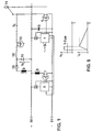
- FIG. 1 shows a circuit diagram of a control circuit for a switch-off thyristor 14.
- the control circuit includes the switch-off circuit and a switch-on circuit.
- the switch-off circuit is essentially formed by a switch-off logic 1, by the energy store 3 and a switch 4.
- the switch 4 is connected to the gate of the GTO 14 and to the energy store 3 and is controlled by the switch-off logic 1.
- the switch-off logic 1 is preferably fed by a series regulator 2 (a commercially available voltage regulator).
- the switch-off logic 1 receives the required control signals, for example via an optical waveguide, indicated by the arrow and the transistor on the left edge of the block of the switch-off logic 1.
- a command sent via the optical waveguide to switch off the GTO 14 is amplified in the logic 1 and forms a voltage on the switch 4 so that it begins to conduct. Because of the polarity of the energy store 3, a current is thus drawn from the gate of the GTO 14. This makes the gate of the GTO negative towards the cathode and the GTO turns off.
- the switch 3 can in particular also comprise a parallel connection of MOSFETs. The same applies to the energy store 3, which can consist of a plurality of EL-KOs connected in parallel.
- a switch-on circuit is also provided. This includes switch-on logic 5, which is fed by the energy store 3 in the same way as the switch-off logic 1 becomes.
- the corresponding series regulator is designated by 6.
- the two logics 1 and 5 are connected to each other in terms of signals. Receives the switch-off logic 1 a command to turn off the GTO 14, so it becomes an activation the switch-on logic 5 prevented. However, if logic 1 receives a switch-on command, the switch-on logic 5 thus forces the switch 7 which it controls for clocking.
- the switch 7 is also arranged between the connections 50 and 51.
- the voltage pulses generated in this way are with the help of Switch 7 series-connected transformer 8, 9 to a rectifier diode 10 transmit an electrical energy storage, preferably an inductor 12 feeds.
- the inductance of the transformer 8, 9 should cover the whole arrangement to keep low inductance as desired, be smaller than the inductance 12. This can be achieved structurally, for example, that the coils 8 and 9 integrated into the board and magnetically coupled with a core. Depending on the required The size of the inductor 12 can also be used as a conductor loop on the circuit board to get integrated.
- the inductance 12 is connected to the via a further switch 13 Gate of the GTO 14 connected.
- the switch 13 separates the switch-on circuit Turn off and off the gate of the GTO.
- FIG. 5 shows such a voltage pulse V T , which is transmitted via the transformer 8, 9.
- the voltage pulse is rectified by the diode 10 and converted into a current in the inductor 12.
- the current can swing over the freewheeling diode 11 arranged between the positive connection 50 and the cathode.
- the current through the inductor 12 has a triangular shape as shown in FIG. 5.
- approximately 200 A to 400 A are required to switch on, which should be maintained for approximately 5 to 15 ⁇ s.
- the GTO 14 still needs a certain holding current to maintain the switched-on state.
- the simplest way to do this is to repeat the switch-on pulse described with a specific frequency f1.
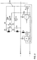
- FIG. 2 shows an embodiment that meets this requirement.
- a second inductance 24 is provided, which is also fed via the transformer via a second secondary winding 20.
- the rectifier diode bears the reference number 21, the free-wheeling diode 22.
- a capacitor 23 is preferably connected in parallel with the free-wheeling diode 22.
- the capacitance 23 enables a slower extraction of energy, so that the repetition frequency can be kept lower and the holding current is nevertheless sufficiently uniform.
- the inductance 24 can be chosen larger than the inductance 12, for example in the range from 10 to 50 ⁇ H.
- a separate transformer and a separate logic can also be provided. In this generation of the holding current, which is separate from the generation of the switch-on pulse, the switch 13 is opened after the ignition of the GTO 14, so that the inductance 12 is separated from the gate.
- a device according to the invention for limiting the holding current in each Operating state comprises a transistor 26, which in the case of FIG Current path between the switch-on circuit and cathode is connected. Is preferred an emitter follower with a bipolar transistor 26 and a base series resistor 25. This device reliably prevents the holding current from being negative Gate-cathode voltage can rise unhindered. With a negative voltage namely, the diode 22 becomes conductive, and the current could thus be unimpeded increase. This is effectively prevented by the device according to the invention.
- the voltage pulse required for generating the holding current can also be tapped directly from the rectified voltage after the diode 10 without a second secondary winding.
- Figure 3 shows a corresponding embodiment.
- the common node of the rectifier diode 10 and the freewheeling diode 11 is connected to the second inductor 24.
- the current rise limiting means bear the reference symbols 27 for the bipolar transistor and 28 for the series resistor.
- a reverse polarity transistor is used and transistor 27 is connected in the gate current path.
- the mode of operation of this embodiment is essentially the same as that of FIG. 2. It works as follows: With a positive gate-cathode voltage, the current from the inductor 4 is divided into a base current and a collector current of the transistor 27. The base current switches the transistor through .
- the inductor 24 is connected directly to the gate of the GTO 14.
- the transistor begins to regulate: In order for the transistor to carry a collector current, its emitter must be around the forward voltage, ie approx. 0.7 V more positive than the base.
- the inductance 24 to be considered as a current source in the first approximation, however, continues to work as a counter voltage.
- the collector voltage becomes negative as soon as the commutation process, ie the GTO 14, forces this.
- U a U EB + Ur.
- U is the voltage across the inductor, UEB denotes the emitter-base voltage UR and the voltage drop across the base resistor.
- FIG. 4 shows a corresponding embodiment.
- a switch-on logic 5a drives two transistors 31 and 30 arranged between the connections 50 and 51.
- the transistor 31 generates a positive voltage pulse, the transistor 30 resets again.
- the generated voltage pulse is passed on to the rectifier diode 10 via a coupling capacitor 32.
- a recharging diode 33 is provided, which is arranged between the cathode of the GTO or the positive connection 50 of the voltage source and the rectifier diode 10. Otherwise, the circuit according to FIG. 4 functions like that already described above.
- FIG. 6 shows an embodiment of the invention in which the switch-off circuit is used to generate the ignition current.
- Logics 1 and 5 are no longer shown for the sake of clarity.
- the circuit works as follows: A charging transistor 36 connects a switchable ignition inductor 35 to the positive terminal 50 before the switch-off transistor 4 is blocked. As a result, a current builds up in the inductor 35, which commutates directly to the gate after the switch 4 has been blocked and thus forms the required ignition pulse.
- the inductance 35 can be selected so that the current dissipates in approximately 5 to 10 microseconds.
- the charging diode 37 connected upstream of the inductance 35 then blocks, and the charging transistor 36 can be blocked again.
- the transistor 36 If the transistor 36 is blocked before the current has decayed, the residual energy can be returned to the energy store 3 via the freewheeling diode 38. In this way, a particularly short and yet fully effective ignition pulse is generated.
- the part of the switch-on circuit which is designed to generate the holding current can be constructed as already described, or the energy required can be transferred from the energy store 3 by means of a storage inductor 34 and the rectifier diode 21 to the energy store 24 by clocking the switch 7. To switch off the GTO 14, a current is drawn from the gate by actuating the switch 4.
- the control circuit explained enables a reduction in the repetition frequency f1 of the voltage pulses for the holding current as soon as a negative gate-cathode voltage occurs at the GTO.
- the loss occurs in the bipolar transistor 26 or 27 of the current increase limiting means, particularly for GTOs highest performance, i.e. those with a high demand for holding current (> 1 A).
- the repetition frequency can be restored after a positive voltage between the gate and cathode of the GTO can be increased again. Thereby achieved one again a higher gate current, so that a complete recommutation of the GTO is ensured.
- a post-ignition pulse in the usual way This eliminates the need for form.
- the gate current can be influenced by influencing the repetition frequency of the voltage pulses can be set.
- the circuit can also be constructed so that the switch-on circuit has its own power supply having.
- the transformer 8, 9 would be omitted in this case at least one additional supply line and an additional energy store are necessary.
- the device according to the invention allows the holding current to be reliable to restrict.
- a control circuit equipped with this device has a compact and extremely efficient structure, so that the circuit arrangement becomes low inductive.
- the circuit is therefore also for hard-controlled GTOs especially suitable.
Landscapes
- Engineering & Computer Science (AREA)
- Power Engineering (AREA)
- Power Conversion In General (AREA)
- Thyristors (AREA)
Abstract
Es wird eine Vorrichtung zur Begrenzung des Haltestromes eines GTOs angegeben.
Die Vorrichtung ist Teil einer Ansteuerschaltung zum Ein- und Ausschalten
des GTOs und dadurch gekennzeichnet, dass ein Transistor in den
Strompfad zwischen der Einschaltschaltung der Ansteuerschaltung und entweder
dem Gate oder der Kathode des Abschaltthyristors geschaltet ist, wobei
die Steuerelektrode des Transistors mit der Kathode bzw. dem Gate des
Abschaltthyristors verbunden ist. Im ersten Fall handelt es sich vorzugsweise
um einen pnp-Transistor im zweiten Fall um einen npn-Transistor.

Description
Die Erfindung bezieht sich auf das Gebiet der Leistungselektronik. Sie geht aus von einer Vorrichtung zum Begrenzen eines Haltestromes eines Abschaltthyristors nach dem Oberbegriff des unabhängigen Anspruches.The invention relates to the field of power electronics. It starts from a device for limiting a holding current of a shutdown thyristor the preamble of the independent claim.
Abschaltthyristoren oder GTOs benötigen einen nicht unerheblichen Haltestrom am Gate, um den eingeschalteten Zustand aufrecht zu erhalten. Bei GTOs höchster Leistung wie z.B. einem 3 kA/4.5 kV Typ werden beispielsweise zwischen 4 A und 8 A Haltestrom im eingeschalteten Zustand benötigt, damit die Einrastbedingungen auch nach Einbrüchen im Anodenstrom und nach Kommutiervorgängen zwischen dem GTO und der antiparallelen Diode zuverlässig wiederhergestellt wird. Zum Wiederaufkommutieren ist es zudem oft notwendig, einen erhöhten Stromstoss zur Verfügung zu stellen. Beim Stand der Technik wird zu diesem Zweck häufig erneut ein Einschaltpuls angelegt. Der Leistungsbedarf, das Bauvolumen und auch der Kühlungsbedarf der Ansteuerschaltungen wird dadurch deutlich vergrössert.Switch-off thyristors or GTOs require a not inconsiderable holding current on Gate to keep it on. With top performance GTOs such as. a 3 kA / 4.5 kV type, for example, between 4 A and 8 A Holding current required when switched on, so that the latching conditions even after dips in the anode current and after commutation between the GTO and the anti-parallel diode is reliably restored. To the Recommutation is often necessary to increase the current surge To make available. For this purpose, the state of the art is often used again a switch-on pulse is applied. The power requirement, the construction volume and also the This significantly increases the cooling requirements of the control circuits.
Gerade aber für sogenannt hart angesteuerte GTOs, wäre es wünschenswert, eine möglichst kompakte Ansteuerschaltung zur Verfügung zu haben, damit diese in unmittelbarer Nähe des GTOs angeordnet werden kann. Eine Ansteuerschaltung für hart angesteuerte GTOs wird in der Europäischen Patentanmeldung EP 0 489 945 A1 des gleichen Erfinders beschrieben. Bei der harten Ansteuerung eines Abschaltthyristors wird im Gegensatz zur konventionellen Ansteuerung ein höherer und sehr viel steilerer Strom zum Ausschalten des GTOs an das Gate angelegt wird. Ausserdem sind Mittel zum Erzeugen eines Einschaltstromes vorgesehen. Diese Mittel erzeugen einen Strom zum Einschalten des GTO und einen Haltestrom zum Aufrechterhalten des eingeschalteten Zustandes. Die Mittel umfassen jeweils Kondensatoren, in denen die notwendige Energie gespeichert wird und mit Hilfe von Schaltern bedarfsweise entnommen wird.But especially for so-called hard driven GTOs, it would be desirable to have one to have the most compact possible control circuit available so that this in can be arranged in the immediate vicinity of the GTO. A control circuit for hard-driven GTOs are described in European patent application EP 0 489 945 A1 described by the same inventor. When driving a shutdown thyristor hard in contrast to conventional control becomes a higher and a lot steeper current is applied to the gate to turn off the GTO. Furthermore means for generating an inrush current are provided. Generate these funds a current to turn on the GTO and a hold current to maintain of the switched on state. The means each include capacitors in which the necessary energy is stored and if necessary with the help of switches is removed.
Aus der nicht vorveröffentlichten Deutschen Patentanmeldung mit dem Aktenzeichen 197 08 873.2, ebenfalls des selben Erfinders, ist ferner eine räumliche Anordnung für eine Ansteuereinheit bekannt. Um die harte Ansteuerung zu realisieren, sind nämlich Anordnungen mit sehr niederinduktivem Aufbau gefragt. Zu diesem Zweck wird in der nicht vorveröffentlichten Patentanmeldung vorgeschlagen, die Bauelement in unmittelbarer Nähe des GTO anzuordnen. Grosse Aufbauten komplizieren zudem durch die enge Verknüpfung mit dem GTO den gesamten Stromrichter bezüglich Stabilität und Gesamtbauvolumen. Deshalb ist insbesondere bei hart angesteuerten GTOs notwendig, die Ansteuerschaltungen klein, zuverlässig und mit hohen Wirkungsgrad versehen aufzubauen.From the unpublished German patent application with the file number 197 08 873.2, also by the same inventor, is also a spatial arrangement known for a control unit. To implement the hard control, arrangements with a very low-inductance structure are in demand. To this Purpose is proposed in the unpublished patent application which Arrange component in the immediate vicinity of the GTO. Complicate large structures also through the close link with the GTO the entire converter in terms of stability and overall construction volume. That is why hard-controlled GTOs necessary, the control circuits small, reliable and build with high efficiency.
Im Besonderen, wenn der Strom im eingeschalteten Zustand auf die Antiparalleldiode kommutiert hat, liegt an der Anode des GTOs eine bezüglich der Kathode negative Spannung. Diese wird durch die innere Struktur auf das Gate übertragen. Aufgrund der negativen Spannung des Gate gegenüber der Kathode würde der Haltestrom in das Gate ohne geeignete Massnahmen ungehindert ansteigen.Especially when the current is switched on to the anti-parallel diode has commutated, there is a negative on the anode of the GTO with respect to the cathode Tension. This is transferred to the gate through the internal structure. Because of the negative voltage of the gate against the cathode would be the holding current climb unhindered without suitable measures.
Aufgabe der Erfindung ist es deshalb, eine Vorrichtung zur Begrenzung des Haltestromes anzugeben, die einfach aufgebaut ist und trotzdem zuverlässig funktioniert. Ausserdem soll eine Ansteuerschaltung, zu der die Vorrichtung gehört, kompakt, zuverlässig und mit einem hohen Wirkungsgrad versehen aufgebaut sein. Diese Aufgabe wird durch die Merkmale des unabhängigen Anspruchs gelöst.The object of the invention is therefore a device for limiting the holding current specify that is simple and yet works reliably. In addition, a control circuit to which the device belongs should be compact, be built reliably and with high efficiency. This The object is solved by the features of the independent claim.
Die erfindungsgemässe Vorrichtung ist dadurch gekennzeichnet, dass ein Transistor in den Strompfad zwischen der Einschaltschaltung der Ansteuerschaltung und entweder dem Gate oder der Kathode des Abschaltthyristors geschaltet ist, wobei die Steuerelektrode des Transistors mit der Kathode bzw. dem Gate des Abschaltthyristors verbunden ist. Im ersten Fall handelt es sich vorzugsweise um einen pnp-Transistor im zweiten Fall um einen npn-Transistor.The device according to the invention is characterized in that a transistor in the current path between the turn-on circuit of the drive circuit and either the gate or the cathode of the turn-off thyristor is connected, the Control electrode of the transistor with the cathode or the gate of the turn-off thyristor connected is. In the first case, it is preferably a pnp transistor in the second case an npn transistor.
Die Ansteuerschaltung umfasst eine Einschaltschaltung und eine Ausschaltschaltung. Der Einschaltstrom und der Haltestrom werden aus Spannungsimpulsen erzeugt, die mit Hilfe eines elektrischen Energiespeichers in Ströme umgewandelt werden. Schaltungstechnisch ist es von besonderem Vorteil, wenn die benötigten Spannungspulse derselben Energiequelle, bzw. demselben Energiespeicher entnommen werden wie der für die Erzeugung des Ausschaltstromes benötigte Puls. Der Haltestrom wird vorzugsweise durch Wiederholen von Spannungspulsen erzeugt. Die Wiederholfrequenz dieser Spannungspulse kann dann je nach Bedarf erhöht oder verringert werden. Insbesondere wenn die Gate-Kathoden-Spannung negativ wird, wird die Frequenz reduziert, um bei erneut positiver Spannung wieder erhöht zu werden. Eine erfindungsgemässe Ansteuerschaltung umfasst somit im Rahmen der Einschaltschaltung mindestens einen elektrischen Energiespeicher, der die Spannungspulse in Ströme umwandelt. Es können ein gemeinsamer Energiespeicher für den Einschaltstrom und für den Haltestrom oder auch getrennte Energiespeicher vorgesehen sein. Die Übertragung der benötigten Energie aus dem Energiespeicher der Ausschaltschaltung auf die Energiespeicher der Einschaltschaltung kann entweder mittels induktiver Kopplung oder mittels kapazitiver Kopplung erfolgen. Besonders bevorzugt wird eine Ansteuerschaltung, bei der die elektrische Speisung der benötigten Logikschaltungen und der anderen Bauteile auf dem erwähnten Energiespeicher der Ausschaltschaltung basiert.The control circuit comprises a switch-on circuit and a switch-off circuit. The inrush current and the holding current are generated from voltage pulses, which are converted into currents with the help of an electrical energy store become. In terms of circuitry, it is particularly advantageous if the required Voltage pulses taken from the same energy source or the same energy store become like the pulse needed to generate the breaking current. The holding current is preferably generated by repeating voltage pulses. The repetition frequency of these voltage pulses can then be increased as required or be reduced. Especially when the gate cathode voltage is negative the frequency is reduced to again when the voltage is positive again to be raised. A control circuit according to the invention thus includes Frame of the switch-on circuit at least one electrical energy storage device converts the voltage pulses into currents. It can be a common energy storage for the inrush current and for the holding current or separate energy storage be provided. The transfer of the required energy from the Energy storage of the switch-off circuit on the energy storage of the switch-on circuit can either by inductive coupling or by capacitive coupling respectively. A control circuit in which the electrical Supply of the required logic circuits and the other components on the mentioned Energy storage of the switch-off circuit is based.
Mit dem erfindungsgemässen Vorrichtung kann der Haltestrom insbesondere auch dann, wenn eine bezüglich der Kathode negative Spannung am Gate anliegt, zuverlässig und nahezu ohne Verluste begrenzt werden. Der Aufbau der erfindungsgemässen Vorrichtung ist sehr einfach. Der schaltungstechnische Aufwand einer nach der Erfindung aufgebauten Ansteuerschaltung kann somit äusserst gering gehalten werden. Damit ist es möglich, die Ansteuerschaltung sehr nahe beim GTO anzuordnen und die Induktivität wie gewünscht gering zu haltenWith the device according to the invention, the holding current can in particular also when a negative voltage with respect to the cathode is present at the gate, reliably and be limited with almost no losses. The structure of the invention Device is very simple. The circuitry effort one after Control circuit constructed according to the invention can thus be kept extremely low become. This makes it possible to arrange the control circuit very close to the GTO and keep the inductance low as desired
Weitere vorteilhafte Ausführungsformen ergeben sich aus den entsprechenden abhängigen Ansprüchen.Further advantageous embodiments result from the corresponding dependent ones Claims.
Nachfolgend wird die Erfindung anhand von Ausführungsbeispielen im Zusammenhang mit den Zeichnungen näher erläutert.In the following, the invention is described in connection with exemplary embodiments explained in more detail with the drawings.
Es zeigen:
- Fig. 1
- Ein Schaltbild zur Erläuterung der Funktion einer Ansteuereinheit für einen GTO;
- Fig. 2
- Ein Schaltbild einer Ausführungsform der Erfindung;
- Fig. 3
- Ein Schaltbild einer weiteren Ausführungsform der Erfindung;
- Fig. 4
- Ein Schaltbild einer dritten Ausführungsform der Erfindung;
- Fig. 5
- Eine schematische Darstellung des Spannungspulses und des dadurch erzeugten Stromes;
- Fig. 6
- Ein Schaltbild einer vierten Ausführungsform der Erfindung.
- Fig. 1
- A circuit diagram to explain the function of a control unit for a GTO;
- Fig. 2
- A circuit diagram of an embodiment of the invention;
- Fig. 3
- A circuit diagram of another embodiment of the invention;
- Fig. 4
- A circuit diagram of a third embodiment of the invention;
- Fig. 5
- A schematic representation of the voltage pulse and the current generated thereby;
- Fig. 6
- A circuit diagram of a fourth embodiment of the invention.
Die in den Zeichnungen verwendeten Bezugszeichen und deren Bedeutung sind in der Bezugszeichenliste zusammengefasst aufgelistet. Grundsätzlich sind in den Figuren gleiche Teile mit gleichen Bezugszeichen versehen.The reference symbols used in the drawings and their meaning are in the list of reference symbols is summarized. Basically are in the figures Identical parts with the same reference numerals.
Figur 1 zeigt ein Schaltbild einer Ansteuerschaltung für einen Abschaltthyristor 14.
Mit 50 und 51 sind die Plus- und Minusanschlüsse einer Spannungsquelle mit z.B. 20
V Ausgangsspannung bezeichnet. Von dieser Spannungsquelle wird ein zu einer
Ausschaltschaltung gehörender Energiespeicher 3 gespeist. Der Energiespeicher 3
kann insbesondere in Form einer Elektrolytkodensatorbank ausgebildet sein. Die
Ansteuerschaltung umfasst neben der Ausschaltschaltung und eine Einschaltschaltung.
Die Ausschaltschaltung wird im wesentlichen gebildet durch eine Ausschaltlogik
1, durch den Energiespeicher 3 und einen Schalter 4. Der Schalter 4 ist an das
Gate des GTO 14 und an den Energiespeicher 3 angeschlossen und wird von der
Ausschaltlogik 1 angesteuert. Die Ausschaltlogik 1 wird vorzugsweise von einem
Längsregler 2 (ein handelsüblicher Spannungsregler) gespeist. Die benötigten Steuersignale
empfängt die Ausschaltlogik 1 beispielsweise über einen Lichtwellenleiter,
angedeutet durch den Pfeil und den Transistor am linken Rand des Blockes der Ausschaltlogik
1. Ein über den Lichtwellenleiter gesandter Befehl, den GTO 14 auszuschalten,
wird in der Logik 1 verstärkt und bildet eine Spannung an dem Schalter 4,
so dass dieser zu leiten beginnt. Aufgrund der Polarität des Energiespeichers 3 wird
somit ein Strom aus dem Gate des GTOs 14 gezogen. Dadurch wird das Gate des
GTOs gegenüber der Kathode negativ, und der GTO schaltet aus. Der Schalter 3
kann insbesondere auch eine Parallelschaltung von MOSFETs umfassen. Analoges
gilt für den Energiespeicher 3, der aus eine Mehrzahl von parallel geschalteten EL-KOs
bestehen kann. FIG. 1 shows a circuit diagram of a control circuit for a switch-
Ausserdem ist eine Einschaltschaltung vorgesehen. Diese umfasst eine Einschaltlogik
5, die in gleicher Weise wie die Ausschaltlogik 1 von dem Energiespeicher 3 gespeist
wird. Der entsprechende Längsregler ist mit 6 bezeichnet. Die beiden Logiken
1 und 5 sind signalmässig miteinander verbunden. Empfängt die Ausschaltlogik 1
einen Befehl zum Ausschalten des GTOs 14, so wird auf diese Weise eine Aktivierung
der Einschaltlogik 5 unterbunden. Empfängt die Logik 1 jedoch einen Einschaltbefehl,
so zwingt die Einschaltlogik 5 den von ihr angesteuerten Schalter 7
zum Takten. Der Schalter 7 ist ebenfalls zwischen den Anschlüssen 50 und 51 angeordnet.
Die auf diese Weise erzeugten Spannungspulse werden mit Hilfe des zum
Schalter 7 in Serie geschalteten Transformators 8, 9 zu einer Gleichrichter Diode 10
übertragen, die einen elektrischen Energiespeicher, vorzugsweise eine Induktivität
12 speist. Die Induktivität des Transformators 8, 9 sollte, um die ganze Anordnung
wie gewünscht niederinduktiv zu halten, kleiner sein als die Induktivität 12. Dies
kann baulich beispielsweise dadurch erreicht werden, dass die Spulen 8 und 9 auf
der Platine integriert und mit einem Kern magnetisch gekoppelt werden. Je nach geforderter
Grösse der Induktivität 12 kann auch sie als Leiterschleife auf der Platine
integriert werden. Die Induktivität 12 ist über einen weiteren Schalter 13 mit dem
Gate des GTO 14 verbunden. Der Schalter 13 trennt die Einschaltschaltung beim
Ausschalten und im ausgeschalteten Zustand von dem Gate des GTO.A switch-on circuit is also provided. This includes switch-on
Figur 5 zeigt einen solchen Spannungspuls VT, der über den Transformator 8, 9 übertragen
wird. Sekundärseitig wird der Spannungspuls durch die Diode 10 gleichgerichtet
und in der Induktivität 12 in einen Strom umgewandelt. Über die zwischen
Plusanschluss 50 und Kathode angeordnete Freilaufdiode 11 kann der Strom umschwingen.
Der Strom durch die Induktivität 12 hat in erster Näherung eine Dreiecksform
wie in Figur 5 dargestellt. Für einen 3 kA, 4.5 kV GTO werden zum Einschalten
ca. 200 A bis 400 A benötigt, die während ca. 5 bis 15 µs aufrecht erhalten
werden sollten. Daraus ergeben sich beispielhafte Werte für die Induktivität 12 im
Bereich von 100 nH. Nach dem Einschalten benötigt der GTO 14 aber noch einen
gewissen Haltestrom, um den eingeschalteten Zustand aufrecht zu erhalten. Am einfachsten
kann dies dadurch erfolgen, dass der beschriebene Einschaltpuls mit einer
bestimmten Frequenz f1 wiederholt wird. FIG. 5 shows such a voltage pulse V T , which is transmitted via the
Der Strombedarf zum Zünden einerseits und zum Aufrechterhalten des gezündeten
Zustandes andererseits ist sehr unterschiedlich. Zum Zünden sind für GTOs höchster
Leistung wie erwähnt ca. 200 A notwendig, während der Haltestrom lediglich
ca. 2 A betragen muss. Aus diesem Grund wäre es vorteilhaft, wenn der Haltestrom
mit weniger Leistung erzeugt werden könnte als durch Wiederholen des Einschaltpulses.
Figur 2 zeigt ein Ausführungsbeispiel, das diesem Erfordernis gerecht wird.
Es ist eine zweite Induktivität 24 vorgesehen, die ebenfalls über den Transformator
via eine zweite Sekundärwicklung 20 gespeist wird. Die Gleichrichterdiode trägt die
Bezugsziffer 21, die Freilaufdiode 22. Vorzugsweise ist parallel zu der Freilaufdiode
22 eine Kapazität 23 geschaltet. Die Kapazität 23 ermöglicht eine langsamere Energieentnahme,
so dass die Wiederholfrequenz kleiner gehalten werden kann und der
Haltestrom dennoch ausreichend gleichmässig ist. Dadurch kann die Induktivität 24
grösser gewählt werden als die Induktivität 12, z.B. im Bereich von 10 bis 50 µH. Anstelle
einer zweiten Sekundärwicklung 22 kann auch ein eigener Transformator und
eine eigene Logik vorgesehen sein. Bei dieser von der Erzeugung des Einschaltpulses
getrennten Erzeugung des Haltestromes wird der Schalter 13 nach dem Zünden
des GTO 14 geöffnet, so dass die Induktivität 12 vom Gate getrennt ist.The current requirement for ignition on the one hand and for maintaining the ignited state on the other hand is very different. As mentioned, approx. 200 A are required to ignite GTOs with the highest output, while the holding current only has to be approx. 2 A. For this reason, it would be advantageous if the holding current could be generated with less power than by repeating the switch-on pulse. Figure 2 shows an embodiment that meets this requirement. A
Im Falle der getrennten Erzeugung des Haltestromes sind zwischen das Gate und
die Kathode des GTOs 14 aktive Stromanstiegsbegrenzungsmittel 25, 26 geschaltet
sind. Eine erfindungsgemässe Vorrichtung zur Begrenzung des Haltestromes in jedem
Betriebszustand umfasst einen Transistor 26, der im Falle der Figur 2 in den
Strompfad zwischen Einschaltschaltung und Kathode geschaltet ist. Bevorzugt wird
ein Emitterfolger mit einem Bipolartransistor 26 und einem Basisvorwiderstand 25.
Diese Vorrichtung verhindert zuverlässig, dass der Haltestrom bei einer negativen
Gate-Kathoden-Spannung ungehindert ansteigen kann. Bei einer negativen Spannung
wird die Diode 22 nämlich leitend, und damit könnte der Strom ungehindert
ansteigen. Dies wird durch die erfindungsgemässe Vorrichtung wirksam verhindert.In the case of separate generation of the holding current are between the gate and
the cathode of the
Der für die Erzeugung des Haltestromes benötigte Spannungspuls kann auch ohne
eine zweite Sekundärwicklung direkt an der gleichgerichteten Spannung nach der
Diode 10 abgegriffen werden. Figur 3 zeigt ein entsprechenden Ausführungsbeispiel.
Der gemeinsame Knotenpunkt der Gleichrichterdiode 10 und der Freilaufdiode
11 ist mit der zweiten Induktivität 24 verbunden. Die Stromanstiegsbegrenzungsmittel
tragen die Bezugszeichen 27 für den Bipolartransistor und 28 für den
Vorwiderstand. In diesem Ausführungsbeispiel wird ein Transistor umgekehrter
Polarität verwendet, und der Transistor 27 ist in den Gatestrompfad geschaltet. Die
Funktionsweise dieser Ausführungsform ist im wesentlichen dieselbe wie diejenige
nach Figur 2. Sie funktioniert wie folgt: Bei positiver Gate-Kathoden-Spannung teilt
sich der Strom aus der Induktivität 4 in einen Basisstrom und einen Kollektorstrom
des Transistors 27. Der Basisstrom schaltet den Transistor durch. Somit wird die Induktivität
24 direkt mit dem Gate des GTO 14 verbunden. Bei negativer Gate-Kathoden-Spannung
beginnt der Transistor zu regeln: Damit der Transistor einen
Kollektorstrom führen kann, muss sein Emitter um die Flussspannung, d.h. ca. 0.7 V
positiver sein als die Basis. Die in erster Näherung als Stromquelle zu betrachtende
Induktivität 24 arbeitet aber weiterhin als Gegenspannung. Die Kollektrospannung
wird negativ, sobald der Kommutierungsvorgang, d.h. der GTO 14 dies erzwingt.
Trotzdem fliesst der Strom aus der Induktivität 24 zum grossen Teil weiter über die
Emitter-Kollektor-Strecke. Dieser Strom wird wirksam begrenzt, weil der Transistor
dies durch die Regelbedingung Uein=UEB + uR verhindert. Uein bezeichnet die Spannung
über der Induktivität, UEB die Emitter-Basis-Spannung und UR den Spannungsabfall
am Basisvorwiderstand. Die Vorrichtung nach Figur 2 mit dem npn-Transistor
26 anstelle des erläuterten pnp-Transistors 27 funktioniert analog.The voltage pulse required for generating the holding current can also be tapped directly from the rectified voltage after the
Anstelle einer induktiven Kopplung mit Hilfe eines Transistors ist auch eine kapazitive
Kopplung mit Kondensatoren möglich. Figur 4 zeigt ein entsprechendes Ausführungsbeispiel.
Eine Einschaltlogik 5a steuert zwei zwischen den Anschlüssen 50
und 51 angeordnete Transistoren 31 und 30 an. Der Transistor 31 erzeugt einen positiven
Spannungspuls, der Transistor 30 setzt wieder zurück. Über einen Koppelkondensator
32 wird der erzeugte Spannungspuls an die Gleichrichterdiode 10 weitergegeben.
Ausserdem ist eine Rückladediode 33 vorgesehen, die zwischen der Kathode
des GTO bzw. dem Plusanschluss 50 der Spannungsquelle und der Gleichrichterdiode
10 angeordnet ist. Im übrigen funktioniert die Schaltung nach Figur 4 wie
die bereits weiter oben beschriebenen.Instead of inductive coupling using a transistor, capacitive coupling with capacitors is also possible. Figure 4 shows a corresponding embodiment. A switch-on
Figur 6 zeigt eine Ausführungsform der Erfindung, bei der zur Erzeugung des
Zündstromes die Ausschaltschaltung zu Hilfe genommen wird. Die Logiken 1 und 5
sind der Übersichtlichkeit halber nicht mehr dargestellt. Die Schaltung funktioniert
wie folgt: Ein Ladetransistor 36 verbindet eine zuschaltbare Zündinduktivität 35 mit
dem Plusanschluss 50 bevor der Ausschalttransistor 4 gesperrt wird. Infolgedessen
baut sich in der Induktivität 35 ein Strom auf, der nach Sperren des Schalters 4 direkt
auf das Gate kommutiert und so den geforderten Zündimpuls bildet. Die Induktivität
35 kann so gewählt werden, dass sich der Strom in ca. 5 bis 10 µs abbaut. Danach
blockiert die der Induktivität 35 vorgeschaltete Ladediode 37, und der Ladetransistor
36 kann wieder gesperrt werden. Falls der Transistor 36 vor Abklingen des
Stromes gesperrt wird, so kann die Restenergie über die Freilaufdiode 38 in den
Energiespeicher 3 zurückgegeben werden. Auf diese Weise wird ein besonders kurzer
und dennoch voll wirksamer Zündimpuls erzeugt. Der Teil der Einschaltschaltung,
der für die Erzeugung des Haltestromes ausgebildet ist, kann wie bereits beschrieben
aufgebaut sein, oder die benötigte Energie kann aus dem Energiespeicher
3 mittels einer Speicherinduktivität 34 und der Gleichrichterdiode 21 durch Taktung
des Schalters 7 an den Energiespeicher 24 übergeben werden. Zum Ausschalten des
GTOs 14 wird durch Betätigen des Schalters 4 aus dem Gate ein Strom gezogen. FIG. 6 shows an embodiment of the invention in which the switch-off circuit is used to generate the ignition current.
In der vorstehenden Beschreibung wurden verschiedene Varianten der Energiekopplung und Speisung angegeben, die zwar nur anhand einzelner Figuren erläutert wurden, aber selbstverständlich fast beliebig miteinander kombinierbar sind, je nachdem, wo schaltungstechnisch ein Schwergewicht gebildet werden soll.In the above description, different variants of the energy coupling have been described and supply specified, which is only explained with reference to individual figures were, but can of course be combined with each other in almost any way, depending according to where a heavyweight is to be formed in terms of circuitry.
Die erläuterte Ansteuerschaltung ermöglicht eine Reduktion der Wiederholfrequenz
f1 der Spannungspulse für den Haltestrom, sobald eine negative Gate-Kathoden-Spannung
am GTO auftritt. In der Folge wird der auftretende Verlust im Bipolartransistor
26 oder 27 der Stromanstiegsbegrenzungsmittel insbesondere bei GTOs
höchster Leistung, d.h. solchen mit einem hohen Bedarf an Haltestrom (> 1 A), reduziert.
Die Wiederholfrequenz kann nach Wiederherstellen einer positiven Spannung
zwischen Gate und Kathode des GTOs wieder erhöht werden. Dadurch erreicht
man wieder einen höheren Gatestrom, so dass ein lückenloses Wiederaufkommutieren
des GTOs sichergestellt wird. Ein Nachzündimpuls in der bisher üblichen
Form wird dadurch überflüssig. Damit verschwindet auch die Gefahr, dass der
Nachzündimpuls zum falschen Zeitpunkt auftritt und auch alle übrigen mit der genauen
Detektion des korrekten Zeitpunktes des Nachzündens verbundenen Probleme.
Ausserdem kann die EMV-Immunität der Anordnung auf diese Weise erhöht
werden. Ganz allgemein kann der Gatestrom durch eine Beeinflussung der Wiederholfrequenz
der Spannungspulse eingestellt werden. The control circuit explained enables a reduction in the repetition frequency
f1 of the voltage pulses for the holding current as soon as a negative gate-cathode voltage
occurs at the GTO. As a result, the loss occurs in the
Vorgängig wurde erläutert, dass der zur Erzeugung des Einschaltstromes bzw. des
Haltestromes benötigte Spannungspuls demselben Energiespeicher 3 entnommen
wird wie der für den Ausschaltstrom benötigte Impuls. Die Schaltung kann aber
auch so aufgebaut sein, dass die Einschaltschaltung eine eigene Spannungsversorgung
aufweist. Der Transformator 8, 9 würde in diesem Fall entfallen, dafür wäre
mindestens eine weitere Versorgungsleitung und ein weiterer Energiespeicher notwendig.It was previously explained that the for generating the inrush current or
Holding current required voltage pulse taken from the
Insgesamt erlaubt die erfindungsgemässe Vorrichtung, den Haltestrom zuverlässig zu beschränken. Eine mit dieser Vorrichtung ausgestattete Ansteuerschaltung weist einen kompakten und äusserst effizienten Aufbau auf, so dass die Schaltungsanordnung niederinduktiv wird. Somit ist die Schaltung auch für hart angesteuerte GTOs speziell geeignet. Overall, the device according to the invention allows the holding current to be reliable to restrict. A control circuit equipped with this device has a compact and extremely efficient structure, so that the circuit arrangement becomes low inductive. The circuit is therefore also for hard-controlled GTOs especially suitable.
- 11
- AusschaltlogikSwitch-off logic
- 22nd
- LängsreglerSeries regulator
- 33rd
- Energiespeicher, AusschaltkondensatorbankEnergy storage, turn-off capacitor bank
- 44th
- Schaltercounter
- 5, 5a5, 5a
- EinschaltlogikStartup logic
- 66
- LängsreglerSeries regulator
- 77
- Schaltercounter
- 88th
- Primärwicklung des TransformatorsPrimary winding of the transformer
- 99
- Sekundärwicklung des TransformatorsSecondary winding of the transformer
- 1010th
- GleichrichterdiodeRectifier diode
- 1111
- FreilaufdiodeFree-wheeling diode
- 1212th
- SpeicherinduktivitätMemory inductance
- 1313
- Schaltercounter
- 1414
- GTOGTO
- 2020th
- Sekundärwicklung des TransformatorsSecondary winding of the transformer
- 2121
- GleichrichterdiodeRectifier diode
- 2222
- FreilaufdiodeFree-wheeling diode
- 2323
- SpeicherkondensatorStorage capacitor
- 2424th
- SpeicherinduktivitätMemory inductance
- 2525th
- BasiswiderstandBase resistance
- 2626
- BipolartransistorBipolar transistor
- 2727
- BipolartransistorBipolar transistor
- 2828
- BasiswiderstandBase resistance
- 3030th
- Schaltercounter
- 3131
- Schaltercounter
- 3232
- KoppelkondensatorCoupling capacitor
- 3333
- RückladediodeReloading diode
- 3434
- SpeicherinduktivitätMemory inductance
- 3535
- ZündinduktivitätIgnition inductance
- 3636
- LadetransistorCharging transistor
- 3737
- LadediodeCharging diode
- 3838
- FreilaufdiodeFree-wheeling diode
- 5050
- PlusanschlussPositive connection
- 5151
- MinusanschlussMinus connection
- UEB U EB
- Emitter-BasisspannungBase emitter voltage
- UR U R
-
Spannung am Vorwiderstand 27Voltage across the
series resistor 27 - VT V T
-
Spannung an der Freilaufdiode 22Voltage on the freewheeling
diode 22 - IG I G
- GatestromGate current
Claims (7)
Applications Claiming Priority (2)
| Application Number | Priority Date | Filing Date | Title |
|---|---|---|---|
| DE19731835 | 1997-07-24 | ||
| DE1997131835 DE19731835A1 (en) | 1997-07-24 | 1997-07-24 | Device for limiting the holding current of a shutdown thyristor |
Publications (2)
| Publication Number | Publication Date |
|---|---|
| EP0893883A2 true EP0893883A2 (en) | 1999-01-27 |
| EP0893883A3 EP0893883A3 (en) | 2000-03-29 |
Family
ID=7836759
Family Applications (1)
| Application Number | Title | Priority Date | Filing Date |
|---|---|---|---|
| EP98810626A Withdrawn EP0893883A3 (en) | 1997-07-24 | 1998-07-06 | Device for limiting the hold current of a gate turn-off thyristor |
Country Status (4)
| Country | Link |
|---|---|
| EP (1) | EP0893883A3 (en) |
| JP (1) | JPH1189216A (en) |
| CA (1) | CA2243776A1 (en) |
| DE (1) | DE19731835A1 (en) |
Cited By (1)
| Publication number | Priority date | Publication date | Assignee | Title |
|---|---|---|---|---|
| CN111884638A (en) * | 2020-07-07 | 2020-11-03 | 大力(武汉)环保科技有限公司 | Thyristor interlocking control circuit |
Family Cites Families (7)
| Publication number | Priority date | Publication date | Assignee | Title |
|---|---|---|---|---|
| DE3344435A1 (en) * | 1983-12-08 | 1985-06-20 | Siemens AG, 1000 Berlin und 8000 München | CIRCUIT ARRANGEMENT FOR DRIVING A THYRISTOR WITH A PHOTOTRANSISTOR |
| US4593204A (en) * | 1983-12-27 | 1986-06-03 | General Electric Company | Driver circuits for gate turn-off thyristors and bipolar transistors |
| DE3418657C2 (en) * | 1984-05-17 | 1987-02-12 | Licentia Patent-Verwaltungs-Gmbh, 6000 Frankfurt | Arrangement for controlling high-power turn-off thyristors |
| DE3434607A1 (en) * | 1984-09-18 | 1986-03-27 | Siemens AG, 1000 Berlin und 8000 München | METHOD AND DEVICE FOR OPERATING A SWITCH-OFF HYRISTOR |
| DE3446344A1 (en) * | 1984-12-14 | 1986-06-19 | Licentia Patent-Verwaltungs-Gmbh, 6000 Frankfurt | Device for driving a high-power GTO thyristor |
| DE3509617A1 (en) * | 1985-02-27 | 1986-09-04 | Licentia Patent-Verwaltungs-Gmbh, 6000 Frankfurt | Arrangement for floating, positive drive of relatively high power GTO thyristors |
| DE3523666A1 (en) * | 1985-06-29 | 1987-01-08 | Licentia Gmbh | Circuit arrangement for the floating switching-on of a GTO thyristor or bipolar transistor using an impressed control current |
-
1997
- 1997-07-24 DE DE1997131835 patent/DE19731835A1/en not_active Withdrawn
-
1998
- 1998-07-06 EP EP98810626A patent/EP0893883A3/en not_active Withdrawn
- 1998-07-13 JP JP19688698A patent/JPH1189216A/en active Pending
- 1998-07-20 CA CA 2243776 patent/CA2243776A1/en not_active Abandoned
Cited By (1)
| Publication number | Priority date | Publication date | Assignee | Title |
|---|---|---|---|---|
| CN111884638A (en) * | 2020-07-07 | 2020-11-03 | 大力(武汉)环保科技有限公司 | Thyristor interlocking control circuit |
Also Published As
| Publication number | Publication date |
|---|---|
| EP0893883A3 (en) | 2000-03-29 |
| DE19731835A1 (en) | 1999-02-04 |
| CA2243776A1 (en) | 1999-01-24 |
| JPH1189216A (en) | 1999-03-30 |
Similar Documents
| Publication | Publication Date | Title |
|---|---|---|
| DE69229263T2 (en) | DRIVER CIRCUIT AND METHOD FOR CONTROLLING A HIGH EFFICIENCY SWITCH GATE WITH A HIGH EFFICIENCY USING A STREADED INDUCTIVE TRANSFORMER | |
| DE3639256C2 (en) | ||
| DE69012834T2 (en) | CHARGING DEVICE FOR ELECTRIC ENERGY STORAGE WITH CHARGE CONTROL MEANS. | |
| DE3026040A1 (en) | SWITCH WITH MOS-FET IN SERIES | |
| DE102008032876A1 (en) | Method, circuit arrangement and bridge circuit | |
| DE19746112A1 (en) | Power converter arrangement | |
| DE3702680A1 (en) | METHOD AND CIRCUIT FOR CONTROLLING ELECTROMAGNETIC CONSUMERS | |
| DE4040374A1 (en) | ELECTRIC PULSE POWER SUPPLY | |
| DE3429488C2 (en) | ||
| EP0155059A2 (en) | Circuit arrangement for switching the current in an inductive load | |
| EP1524768B1 (en) | Method and device for controlling a gate turn-off thyristor | |
| DE102015219683B4 (en) | DISCHARGE DEVICE | |
| DE102014213737A1 (en) | Driver circuit and semiconductor device containing the driver circuit | |
| DE2223376A1 (en) | PROTECTIVE CIRCUIT FOR A SWITCHING TRANSISTOR IN THE INDUCTIVE LOAD CIRCUIT | |
| DE3405793A1 (en) | METHOD AND DEVICE FOR SHORT CIRCUIT PROTECTION OF A CONVERTER WITH GTO THYRISTORS | |
| EP0674102B1 (en) | Alternating current ignition with optimized electronic circuit | |
| EP0565667B1 (en) | Gto thyristor circuit | |
| DE60005758T2 (en) | Control circuit for a power semiconductor switch | |
| EP3317967B1 (en) | Circuit assembly for driving a transistor | |
| DE2448218A1 (en) | CHOPPER CIRCUIT | |
| EP1071210B1 (en) | Cicuit arrangement | |
| DE19825801C2 (en) | DC link with high load resistance | |
| DE2724741A1 (en) | Protection circuit for static converter bridge - has second capacitor in series with second diode shunting each of four bridge transistors | |
| DE3611297C2 (en) | ||
| EP1753272A2 (en) | Tranformerless converter circuit, comprising an inductance for a pulsed operation of a dielectric barrier discharge lamp |
Legal Events
| Date | Code | Title | Description |
|---|---|---|---|
| PUAI | Public reference made under article 153(3) epc to a published international application that has entered the european phase |
Free format text: ORIGINAL CODE: 0009012 |
|
| AK | Designated contracting states |
Kind code of ref document: A2 Designated state(s): AT BE CH CY DE DK ES FI FR GB GR IE IT LI LU MC NL PT SE |
|
| AX | Request for extension of the european patent |
Free format text: AL;LT;LV;MK;RO;SI |
|
| PUAL | Search report despatched |
Free format text: ORIGINAL CODE: 0009013 |
|
| AK | Designated contracting states |
Kind code of ref document: A3 Designated state(s): AT BE CH CY DE DK ES FI FR GB GR IE IT LI LU MC NL PT SE |
|
| AX | Request for extension of the european patent |
Free format text: AL;LT;LV;MK;RO;SI |
|
| RAP1 | Party data changed (applicant data changed or rights of an application transferred) |
Owner name: ABB INDUSTRIE AG |
|
| AKX | Designation fees paid | ||
| REG | Reference to a national code |
Ref country code: DE Ref legal event code: 8566 |
|
| STAA | Information on the status of an ep patent application or granted ep patent |
Free format text: STATUS: THE APPLICATION IS DEEMED TO BE WITHDRAWN |
|
| 18D | Application deemed to be withdrawn |
Effective date: 20001010 |