EP0893883A2 - Dispositif servant à limiter le courant de maintien d'un thyristor blocable - Google Patents
Dispositif servant à limiter le courant de maintien d'un thyristor blocable Download PDFInfo
- Publication number
- EP0893883A2 EP0893883A2 EP98810626A EP98810626A EP0893883A2 EP 0893883 A2 EP0893883 A2 EP 0893883A2 EP 98810626 A EP98810626 A EP 98810626A EP 98810626 A EP98810626 A EP 98810626A EP 0893883 A2 EP0893883 A2 EP 0893883A2
- Authority
- EP
- European Patent Office
- Prior art keywords
- switch
- circuit
- current
- thyristor
- gate
- Prior art date
- Legal status (The legal status is an assumption and is not a legal conclusion. Google has not performed a legal analysis and makes no representation as to the accuracy of the status listed.)
- Withdrawn
Links
- 238000004146 energy storage Methods 0.000 claims description 12
- 230000008878 coupling Effects 0.000 claims description 8
- 238000010168 coupling process Methods 0.000 claims description 8
- 238000005859 coupling reaction Methods 0.000 claims description 8
- 238000004804 winding Methods 0.000 claims description 8
- 239000003990 capacitor Substances 0.000 description 7
- 238000010586 diagram Methods 0.000 description 6
- 230000006870 function Effects 0.000 description 3
- 230000001939 inductive effect Effects 0.000 description 3
- 238000010276 construction Methods 0.000 description 2
- 230000003287 optical effect Effects 0.000 description 2
- 230000004913 activation Effects 0.000 description 1
- 239000004020 conductor Substances 0.000 description 1
- 238000001816 cooling Methods 0.000 description 1
- 230000001419 dependent effect Effects 0.000 description 1
- 238000001514 detection method Methods 0.000 description 1
- 239000003792 electrolyte Substances 0.000 description 1
- 238000000605 extraction Methods 0.000 description 1
- 230000036039 immunity Effects 0.000 description 1
- 238000000034 method Methods 0.000 description 1
- 230000008569 process Effects 0.000 description 1
- 230000009467 reduction Effects 0.000 description 1
- 238000011144 upstream manufacturing Methods 0.000 description 1
Images


Classifications
-
- H—ELECTRICITY
- H03—ELECTRONIC CIRCUITRY
- H03K—PULSE TECHNIQUE
- H03K17/00—Electronic switching or gating, i.e. not by contact-making and –breaking
- H03K17/51—Electronic switching or gating, i.e. not by contact-making and –breaking characterised by the components used
- H03K17/56—Electronic switching or gating, i.e. not by contact-making and –breaking characterised by the components used by the use, as active elements, of semiconductor devices
- H03K17/72—Electronic switching or gating, i.e. not by contact-making and –breaking characterised by the components used by the use, as active elements, of semiconductor devices having more than two PN junctions; having more than three electrodes; having more than one electrode connected to the same conductivity region
- H03K17/73—Electronic switching or gating, i.e. not by contact-making and –breaking characterised by the components used by the use, as active elements, of semiconductor devices having more than two PN junctions; having more than three electrodes; having more than one electrode connected to the same conductivity region for DC voltages or currents
-
- H—ELECTRICITY
- H03—ELECTRONIC CIRCUITRY
- H03K—PULSE TECHNIQUE
- H03K17/00—Electronic switching or gating, i.e. not by contact-making and –breaking
- H03K17/51—Electronic switching or gating, i.e. not by contact-making and –breaking characterised by the components used
- H03K17/56—Electronic switching or gating, i.e. not by contact-making and –breaking characterised by the components used by the use, as active elements, of semiconductor devices
- H03K17/72—Electronic switching or gating, i.e. not by contact-making and –breaking characterised by the components used by the use, as active elements, of semiconductor devices having more than two PN junctions; having more than three electrodes; having more than one electrode connected to the same conductivity region
- H03K17/722—Electronic switching or gating, i.e. not by contact-making and –breaking characterised by the components used by the use, as active elements, of semiconductor devices having more than two PN junctions; having more than three electrodes; having more than one electrode connected to the same conductivity region with galvanic isolation between the control circuit and the output circuit
- H03K17/723—Electronic switching or gating, i.e. not by contact-making and –breaking characterised by the components used by the use, as active elements, of semiconductor devices having more than two PN junctions; having more than three electrodes; having more than one electrode connected to the same conductivity region with galvanic isolation between the control circuit and the output circuit using transformer coupling
Definitions
- the invention relates to the field of power electronics. It starts from a device for limiting a holding current of a shutdown thyristor the preamble of the independent claim.
- Switch-off thyristors or GTOs require a not inconsiderable holding current on Gate to keep it on.
- top performance GTOs such as. a 3 kA / 4.5 kV type, for example, between 4 A and 8 A Holding current required when switched on, so that the latching conditions even after dips in the anode current and after commutation between the GTO and the anti-parallel diode is reliably restored.
- To the Recommutation is often necessary to increase the current surge To make available.
- the state of the art is often used again a switch-on pulse is applied. The power requirement, the construction volume and also the This significantly increases the cooling requirements of the control circuits.
- a control circuit for hard-driven GTOs are described in European patent application EP 0 489 945 A1 described by the same inventor.
- driving a shutdown thyristor hard in contrast to conventional control becomes a higher and a lot steeper current is applied to the gate to turn off the GTO.
- means for generating an inrush current are provided. Generate these funds a current to turn on the GTO and a hold current to maintain of the switched on state.
- the means each include capacitors in which the necessary energy is stored and if necessary with the help of switches is removed.
- the object of the invention is therefore a device for limiting the holding current specify that is simple and yet works reliably.
- a control circuit to which the device belongs should be compact, be built reliably and with high efficiency. This The object is solved by the features of the independent claim.
- the device according to the invention is characterized in that a transistor in the current path between the turn-on circuit of the drive circuit and either the gate or the cathode of the turn-off thyristor is connected, the Control electrode of the transistor with the cathode or the gate of the turn-off thyristor connected is.
- a transistor in the current path between the turn-on circuit of the drive circuit and either the gate or the cathode of the turn-off thyristor is connected, the Control electrode of the transistor with the cathode or the gate of the turn-off thyristor connected is.
- it is preferably a pnp transistor in the second case an npn transistor.
- the control circuit comprises a switch-on circuit and a switch-off circuit.
- the inrush current and the holding current are generated from voltage pulses, which are converted into currents with the help of an electrical energy store become.
- the holding current is preferably generated by repeating voltage pulses. The repetition frequency of these voltage pulses can then be increased as required or be reduced. Especially when the gate cathode voltage is negative the frequency is reduced to again when the voltage is positive again to be raised.
- a control circuit according to the invention thus includes Frame of the switch-on circuit at least one electrical energy storage device converts the voltage pulses into currents.
- It can be a common energy storage for the inrush current and for the holding current or separate energy storage be provided.
- the transfer of the required energy from the Energy storage of the switch-off circuit on the energy storage of the switch-on circuit can either by inductive coupling or by capacitive coupling respectively.
- the holding current can in particular also when a negative voltage with respect to the cathode is present at the gate, reliably and be limited with almost no losses.
- the structure of the invention Device is very simple.
- the circuitry effort one after Control circuit constructed according to the invention can thus be kept extremely low become. This makes it possible to arrange the control circuit very close to the GTO and keep the inductance low as desired
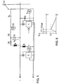
- FIG. 1 shows a circuit diagram of a control circuit for a switch-off thyristor 14.
- the control circuit includes the switch-off circuit and a switch-on circuit.
- the switch-off circuit is essentially formed by a switch-off logic 1, by the energy store 3 and a switch 4.
- the switch 4 is connected to the gate of the GTO 14 and to the energy store 3 and is controlled by the switch-off logic 1.
- the switch-off logic 1 is preferably fed by a series regulator 2 (a commercially available voltage regulator).
- the switch-off logic 1 receives the required control signals, for example via an optical waveguide, indicated by the arrow and the transistor on the left edge of the block of the switch-off logic 1.
- a command sent via the optical waveguide to switch off the GTO 14 is amplified in the logic 1 and forms a voltage on the switch 4 so that it begins to conduct. Because of the polarity of the energy store 3, a current is thus drawn from the gate of the GTO 14. This makes the gate of the GTO negative towards the cathode and the GTO turns off.
- the switch 3 can in particular also comprise a parallel connection of MOSFETs. The same applies to the energy store 3, which can consist of a plurality of EL-KOs connected in parallel.
- a switch-on circuit is also provided. This includes switch-on logic 5, which is fed by the energy store 3 in the same way as the switch-off logic 1 becomes.
- the corresponding series regulator is designated by 6.
- the two logics 1 and 5 are connected to each other in terms of signals. Receives the switch-off logic 1 a command to turn off the GTO 14, so it becomes an activation the switch-on logic 5 prevented. However, if logic 1 receives a switch-on command, the switch-on logic 5 thus forces the switch 7 which it controls for clocking.
- the switch 7 is also arranged between the connections 50 and 51.
- the voltage pulses generated in this way are with the help of Switch 7 series-connected transformer 8, 9 to a rectifier diode 10 transmit an electrical energy storage, preferably an inductor 12 feeds.
- the inductance of the transformer 8, 9 should cover the whole arrangement to keep low inductance as desired, be smaller than the inductance 12. This can be achieved structurally, for example, that the coils 8 and 9 integrated into the board and magnetically coupled with a core. Depending on the required The size of the inductor 12 can also be used as a conductor loop on the circuit board to get integrated.
- the inductance 12 is connected to the via a further switch 13 Gate of the GTO 14 connected.
- the switch 13 separates the switch-on circuit Turn off and off the gate of the GTO.
- FIG. 5 shows such a voltage pulse V T , which is transmitted via the transformer 8, 9.
- the voltage pulse is rectified by the diode 10 and converted into a current in the inductor 12.
- the current can swing over the freewheeling diode 11 arranged between the positive connection 50 and the cathode.
- the current through the inductor 12 has a triangular shape as shown in FIG. 5.
- approximately 200 A to 400 A are required to switch on, which should be maintained for approximately 5 to 15 ⁇ s.
- the GTO 14 still needs a certain holding current to maintain the switched-on state.
- the simplest way to do this is to repeat the switch-on pulse described with a specific frequency f1.
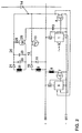
- FIG. 2 shows an embodiment that meets this requirement.
- a second inductance 24 is provided, which is also fed via the transformer via a second secondary winding 20.
- the rectifier diode bears the reference number 21, the free-wheeling diode 22.
- a capacitor 23 is preferably connected in parallel with the free-wheeling diode 22.
- the capacitance 23 enables a slower extraction of energy, so that the repetition frequency can be kept lower and the holding current is nevertheless sufficiently uniform.
- the inductance 24 can be chosen larger than the inductance 12, for example in the range from 10 to 50 ⁇ H.
- a separate transformer and a separate logic can also be provided. In this generation of the holding current, which is separate from the generation of the switch-on pulse, the switch 13 is opened after the ignition of the GTO 14, so that the inductance 12 is separated from the gate.
- a device according to the invention for limiting the holding current in each Operating state comprises a transistor 26, which in the case of FIG Current path between the switch-on circuit and cathode is connected. Is preferred an emitter follower with a bipolar transistor 26 and a base series resistor 25. This device reliably prevents the holding current from being negative Gate-cathode voltage can rise unhindered. With a negative voltage namely, the diode 22 becomes conductive, and the current could thus be unimpeded increase. This is effectively prevented by the device according to the invention.
- the voltage pulse required for generating the holding current can also be tapped directly from the rectified voltage after the diode 10 without a second secondary winding.
- Figure 3 shows a corresponding embodiment.
- the common node of the rectifier diode 10 and the freewheeling diode 11 is connected to the second inductor 24.
- the current rise limiting means bear the reference symbols 27 for the bipolar transistor and 28 for the series resistor.
- a reverse polarity transistor is used and transistor 27 is connected in the gate current path.
- the mode of operation of this embodiment is essentially the same as that of FIG. 2. It works as follows: With a positive gate-cathode voltage, the current from the inductor 4 is divided into a base current and a collector current of the transistor 27. The base current switches the transistor through .
- the inductor 24 is connected directly to the gate of the GTO 14.
- the transistor begins to regulate: In order for the transistor to carry a collector current, its emitter must be around the forward voltage, ie approx. 0.7 V more positive than the base.
- the inductance 24 to be considered as a current source in the first approximation, however, continues to work as a counter voltage.
- the collector voltage becomes negative as soon as the commutation process, ie the GTO 14, forces this.
- U a U EB + Ur.
- U is the voltage across the inductor, UEB denotes the emitter-base voltage UR and the voltage drop across the base resistor.
- FIG. 4 shows a corresponding embodiment.
- a switch-on logic 5a drives two transistors 31 and 30 arranged between the connections 50 and 51.
- the transistor 31 generates a positive voltage pulse, the transistor 30 resets again.
- the generated voltage pulse is passed on to the rectifier diode 10 via a coupling capacitor 32.
- a recharging diode 33 is provided, which is arranged between the cathode of the GTO or the positive connection 50 of the voltage source and the rectifier diode 10. Otherwise, the circuit according to FIG. 4 functions like that already described above.
- FIG. 6 shows an embodiment of the invention in which the switch-off circuit is used to generate the ignition current.
- Logics 1 and 5 are no longer shown for the sake of clarity.
- the circuit works as follows: A charging transistor 36 connects a switchable ignition inductor 35 to the positive terminal 50 before the switch-off transistor 4 is blocked. As a result, a current builds up in the inductor 35, which commutates directly to the gate after the switch 4 has been blocked and thus forms the required ignition pulse.
- the inductance 35 can be selected so that the current dissipates in approximately 5 to 10 microseconds.
- the charging diode 37 connected upstream of the inductance 35 then blocks, and the charging transistor 36 can be blocked again.
- the transistor 36 If the transistor 36 is blocked before the current has decayed, the residual energy can be returned to the energy store 3 via the freewheeling diode 38. In this way, a particularly short and yet fully effective ignition pulse is generated.
- the part of the switch-on circuit which is designed to generate the holding current can be constructed as already described, or the energy required can be transferred from the energy store 3 by means of a storage inductor 34 and the rectifier diode 21 to the energy store 24 by clocking the switch 7. To switch off the GTO 14, a current is drawn from the gate by actuating the switch 4.
- the control circuit explained enables a reduction in the repetition frequency f1 of the voltage pulses for the holding current as soon as a negative gate-cathode voltage occurs at the GTO.
- the loss occurs in the bipolar transistor 26 or 27 of the current increase limiting means, particularly for GTOs highest performance, i.e. those with a high demand for holding current (> 1 A).
- the repetition frequency can be restored after a positive voltage between the gate and cathode of the GTO can be increased again. Thereby achieved one again a higher gate current, so that a complete recommutation of the GTO is ensured.
- a post-ignition pulse in the usual way This eliminates the need for form.
- the gate current can be influenced by influencing the repetition frequency of the voltage pulses can be set.
- the circuit can also be constructed so that the switch-on circuit has its own power supply having.
- the transformer 8, 9 would be omitted in this case at least one additional supply line and an additional energy store are necessary.
- the device according to the invention allows the holding current to be reliable to restrict.
- a control circuit equipped with this device has a compact and extremely efficient structure, so that the circuit arrangement becomes low inductive.
- the circuit is therefore also for hard-controlled GTOs especially suitable.
Landscapes
- Engineering & Computer Science (AREA)
- Power Engineering (AREA)
- Power Conversion In General (AREA)
- Thyristors (AREA)
Applications Claiming Priority (2)
| Application Number | Priority Date | Filing Date | Title |
|---|---|---|---|
| DE19731835 | 1997-07-24 | ||
| DE1997131835 DE19731835A1 (de) | 1997-07-24 | 1997-07-24 | Vorrichtung zum Begrenzen des Haltestromes eines Abschaltthyristors |
Publications (2)
| Publication Number | Publication Date |
|---|---|
| EP0893883A2 true EP0893883A2 (fr) | 1999-01-27 |
| EP0893883A3 EP0893883A3 (fr) | 2000-03-29 |
Family
ID=7836759
Family Applications (1)
| Application Number | Title | Priority Date | Filing Date |
|---|---|---|---|
| EP98810626A Withdrawn EP0893883A3 (fr) | 1997-07-24 | 1998-07-06 | Dispositif servant à limiter le courant de maintien d'un thyristor blocable |
Country Status (4)
| Country | Link |
|---|---|
| EP (1) | EP0893883A3 (fr) |
| JP (1) | JPH1189216A (fr) |
| CA (1) | CA2243776A1 (fr) |
| DE (1) | DE19731835A1 (fr) |
Cited By (1)
| Publication number | Priority date | Publication date | Assignee | Title |
|---|---|---|---|---|
| CN111884638A (zh) * | 2020-07-07 | 2020-11-03 | 大力(武汉)环保科技有限公司 | 一种晶闸管联锁控制电路 |
Family Cites Families (7)
| Publication number | Priority date | Publication date | Assignee | Title |
|---|---|---|---|---|
| DE3344435A1 (de) * | 1983-12-08 | 1985-06-20 | Siemens AG, 1000 Berlin und 8000 München | Schaltungsanordnung zum ansteuern eines thyristors mit einem fototransistor |
| US4593204A (en) * | 1983-12-27 | 1986-06-03 | General Electric Company | Driver circuits for gate turn-off thyristors and bipolar transistors |
| DE3418657C2 (de) * | 1984-05-17 | 1987-02-12 | Licentia Patent-Verwaltungs-Gmbh, 6000 Frankfurt | Anordnung zur Steuerung von Abschaltthyristoren höherer Leistung |
| DE3434607A1 (de) * | 1984-09-18 | 1986-03-27 | Siemens AG, 1000 Berlin und 8000 München | Verfahren und vorrichtung zum betreiben eines abschalthyristors |
| DE3446344A1 (de) * | 1984-12-14 | 1986-06-19 | Licentia Patent-Verwaltungs-Gmbh, 6000 Frankfurt | Einrichtung zur ansteuerung eines hochleistungs-gto-thyristors |
| DE3509617A1 (de) * | 1985-02-27 | 1986-09-04 | Licentia Patent-Verwaltungs-Gmbh, 6000 Frankfurt | Anordnung zur potentialfreien positiven ansteuerung von gto-thyristoren hoeherer leistung |
| DE3523666A1 (de) * | 1985-06-29 | 1987-01-08 | Licentia Gmbh | Schaltungsanordnung zum potentialfreien einschalten eines gto-thyristors oder bipolartransistors mit eingepraegtem steuerstrom |
-
1997
- 1997-07-24 DE DE1997131835 patent/DE19731835A1/de not_active Withdrawn
-
1998
- 1998-07-06 EP EP98810626A patent/EP0893883A3/fr not_active Withdrawn
- 1998-07-13 JP JP19688698A patent/JPH1189216A/ja active Pending
- 1998-07-20 CA CA 2243776 patent/CA2243776A1/fr not_active Abandoned
Cited By (1)
| Publication number | Priority date | Publication date | Assignee | Title |
|---|---|---|---|---|
| CN111884638A (zh) * | 2020-07-07 | 2020-11-03 | 大力(武汉)环保科技有限公司 | 一种晶闸管联锁控制电路 |
Also Published As
| Publication number | Publication date |
|---|---|
| EP0893883A3 (fr) | 2000-03-29 |
| DE19731835A1 (de) | 1999-02-04 |
| CA2243776A1 (fr) | 1999-01-24 |
| JPH1189216A (ja) | 1999-03-30 |
Similar Documents
| Publication | Publication Date | Title |
|---|---|---|
| DE69229263T2 (de) | Treiberschaltkreis und verfahren zur steuerung eines schalters mit schwebendem gate mit hohem wirkungsgrad unter verwendung eines streufeldinduktanz-transformators | |
| DE3639256C2 (fr) | ||
| DE69012834T2 (de) | Ladevorrichtung zur elektrischen energiespeicherung mit ladesteuerungsmitteln. | |
| DE3026040A1 (de) | Schalter mit in serie geschalteten mos-fet | |
| DE102008032876A1 (de) | Verfahren, Schaltungsanordnung und Brückenschaltung | |
| DE19746112A1 (de) | Stromrichteranordnung | |
| DE3702680A1 (de) | Verfahren und schaltung zur ansteuerung von elektromagnetischen verbrauchern | |
| DE4040374A1 (de) | Elektrische impulsstromversorgung | |
| DE3429488C2 (fr) | ||
| EP0155059A2 (fr) | Montage de circuit pour commuter le courant dans un charge inductive | |
| EP1524768B1 (fr) | Procédé et dispositif servant à commander un thyristor blocable | |
| DE102015219683B4 (de) | Entladungsvorrichtung | |
| DE102014213737A1 (de) | Treiberschaltung und Halbleitervorrichtung, die die Treiberschaltung enthält | |
| DE2223376A1 (de) | Schutzschaltung fuer einen schalttransistor im induktiven lastkreis | |
| DE3405793A1 (de) | Verfahren und vorrichtung zum kurzschlussschutz eines stromrichtergeraetes mit gto-thyristoren | |
| EP0674102B1 (fr) | Dispositif d'allumage à courant alternatif avec un circuit électronique optimisé | |
| EP0565667B1 (fr) | Circuit a thyristors gto | |
| DE60005758T2 (de) | Ansteuerschaltung für einen Leistungshalbleiterschalter | |
| EP3317967B1 (fr) | Circuit de commutation destiné à la commande d'un transistor | |
| DE2448218A1 (de) | Zerhackerschaltung | |
| EP1071210B1 (fr) | Montage de circuit | |
| DE19825801C2 (de) | Gleichspannungs-Zwischenkreis mit Hochlast-Widerstand | |
| DE2724741A1 (de) | Schutzbeschaltung fuer jeweils ein stromrichterventil | |
| DE3611297C2 (fr) | ||
| EP1753272A2 (fr) | Circuit convertisseur comprenant une inductance au lieu d' un transformateur, pour l' alimentation pulsée d' une lampe à barrière diélectrique. |
Legal Events
| Date | Code | Title | Description |
|---|---|---|---|
| PUAI | Public reference made under article 153(3) epc to a published international application that has entered the european phase |
Free format text: ORIGINAL CODE: 0009012 |
|
| AK | Designated contracting states |
Kind code of ref document: A2 Designated state(s): AT BE CH CY DE DK ES FI FR GB GR IE IT LI LU MC NL PT SE |
|
| AX | Request for extension of the european patent |
Free format text: AL;LT;LV;MK;RO;SI |
|
| PUAL | Search report despatched |
Free format text: ORIGINAL CODE: 0009013 |
|
| AK | Designated contracting states |
Kind code of ref document: A3 Designated state(s): AT BE CH CY DE DK ES FI FR GB GR IE IT LI LU MC NL PT SE |
|
| AX | Request for extension of the european patent |
Free format text: AL;LT;LV;MK;RO;SI |
|
| RAP1 | Party data changed (applicant data changed or rights of an application transferred) |
Owner name: ABB INDUSTRIE AG |
|
| AKX | Designation fees paid | ||
| REG | Reference to a national code |
Ref country code: DE Ref legal event code: 8566 |
|
| STAA | Information on the status of an ep patent application or granted ep patent |
Free format text: STATUS: THE APPLICATION IS DEEMED TO BE WITHDRAWN |
|
| 18D | Application deemed to be withdrawn |
Effective date: 20001010 |