EP0895339A2 - Stromartsteuereinrichtung und Betriebsverfahren für Leistungsfaktorkorrekturschaltung mit ständig leitendem Modus - Google Patents
Stromartsteuereinrichtung und Betriebsverfahren für Leistungsfaktorkorrekturschaltung mit ständig leitendem Modus Download PDFInfo
- Publication number
- EP0895339A2 EP0895339A2 EP98306014A EP98306014A EP0895339A2 EP 0895339 A2 EP0895339 A2 EP 0895339A2 EP 98306014 A EP98306014 A EP 98306014A EP 98306014 A EP98306014 A EP 98306014A EP 0895339 A2 EP0895339 A2 EP 0895339A2
- Authority
- EP
- European Patent Office
- Prior art keywords
- factor correction
- correction circuit
- power factor
- coupled
- modulator
- Prior art date
- Legal status (The legal status is an assumption and is not a legal conclusion. Google has not performed a legal analysis and makes no representation as to the accuracy of the status listed.)
- Withdrawn
Links
Images




Classifications
-
- H—ELECTRICITY
- H02—GENERATION; CONVERSION OR DISTRIBUTION OF ELECTRIC POWER
- H02M—APPARATUS FOR CONVERSION BETWEEN AC AND AC, BETWEEN AC AND DC, OR BETWEEN DC AND DC, AND FOR USE WITH MAINS OR SIMILAR POWER SUPPLY SYSTEMS; CONVERSION OF DC OR AC INPUT POWER INTO SURGE OUTPUT POWER; CONTROL OR REGULATION THEREOF
- H02M1/00—Details of apparatus for conversion
- H02M1/42—Circuits or arrangements for compensating for or adjusting power factor in converters or inverters
- H02M1/4208—Arrangements for improving power factor of AC input
- H02M1/4225—Arrangements for improving power factor of AC input using a non-isolated boost converter
-
- Y—GENERAL TAGGING OF NEW TECHNOLOGICAL DEVELOPMENTS; GENERAL TAGGING OF CROSS-SECTIONAL TECHNOLOGIES SPANNING OVER SEVERAL SECTIONS OF THE IPC; TECHNICAL SUBJECTS COVERED BY FORMER USPC CROSS-REFERENCE ART COLLECTIONS [XRACs] AND DIGESTS
- Y02—TECHNOLOGIES OR APPLICATIONS FOR MITIGATION OR ADAPTATION AGAINST CLIMATE CHANGE
- Y02B—CLIMATE CHANGE MITIGATION TECHNOLOGIES RELATED TO BUILDINGS, e.g. HOUSING, HOUSE APPLIANCES OR RELATED END-USER APPLICATIONS
- Y02B70/00—Technologies for an efficient end-user side electric power management and consumption
- Y02B70/10—Technologies improving the efficiency by using switched-mode power supplies [SMPS], i.e. efficient power electronics conversion e.g. power factor correction or reduction of losses in power supplies or efficient standby modes
-
- Y—GENERAL TAGGING OF NEW TECHNOLOGICAL DEVELOPMENTS; GENERAL TAGGING OF CROSS-SECTIONAL TECHNOLOGIES SPANNING OVER SEVERAL SECTIONS OF THE IPC; TECHNICAL SUBJECTS COVERED BY FORMER USPC CROSS-REFERENCE ART COLLECTIONS [XRACs] AND DIGESTS
- Y02—TECHNOLOGIES OR APPLICATIONS FOR MITIGATION OR ADAPTATION AGAINST CLIMATE CHANGE
- Y02P—CLIMATE CHANGE MITIGATION TECHNOLOGIES IN THE PRODUCTION OR PROCESSING OF GOODS
- Y02P80/00—Climate change mitigation technologies for sector-wide applications
- Y02P80/10—Efficient use of energy, e.g. using compressed air or pressurized fluid as energy carrier
Definitions
- the present invention is directed, in general, to power conversion and, more specifically, to a current mode controller for a power factor correction circuit operating in a continuous conduction mode (CCM) that handles a relatively wide range of ac input voltages and a method of operating a current mode control in CCM to achieve power factor correction.
- CCM continuous conduction mode
- controllers for switching power supplies required to provide electrical power having both a high power factor and low total harmonic distortion (THD).
- TDD total harmonic distortion
- IEC-1000.3.2 limits the allowable input current THD to 5%, as did the proposed IEC-555 standard. However, for power supplies operating below 600 W, the IEC-1000.3.2 standard allows THD of up to 30%.
- Peak current mode control and average current mode control are two well-known, alternative approaches to regulating the output voltage of switching power supplies to achieve high power factor.
- the industry-preferred approach is average current mode control.
- control voltage (representing an error between the actual output voltage and a reference voltage) is used to produce a reference current to modulate a desired input current. Therefore, the control voltage directly controls the output voltage. Ideally, the control voltage in the conventional average current mode controller directly controls the average value of the current passing through the inductor for the fastest response.
- peak current mode control the switch or inductor current is compared with a threshold signal. THD of less than 5% is realizable if the parameters of the ramp waveform are appropriately selected for the particular line current. Peak current mode control, however, has difficulties in providing low line current distortions over a wide range of AC input voltages and output loads.
- the present invention provides, for use with a power factor correction circuit operable in CCM, a current mode controller, a method of operating a power factor correction circuit to achieve current mode control thereof and a power supply incorporating the controller or the method.
- the controller includes: (1) a modulator, coupled to a switch in the power factor correction circuit, that senses an electrical characteristic and a current passing through the power factor correction circuit and provides, in response thereto, a control signal to the switch and (2) a compensation circuit, coupled to the power factor correction circuit, that provides a compensation signal to the modulator that is a function of a rectified line voltage provided to the power factor correction circuit.
- the compensation signal causes the modulator to modify the control signal to reduce a THD of the power factor correction circuit.
- the present invention introduces the broad concept of employing a harmonic component present in the rectified AC line voltage provided to the power factor correction circuit, in combination with the sensing of a current in the power factor correction circuit, to modify the control signal provided to the switch in the power factor correction circuit. This serves to compensate for variations in input voltage and reduce the THD of the power factor correction circuit.
- the electrical characteristic is an output voltage of the power factor correction circuit.
- the compensation circuit comprises a capacitor coupling the input of the power factor correction circuit to the modulator.
- the capacitor while not necessary to the present invention, provides sign and phase adjustment to the compensation signal.
- the modulator comprises an amplifier and a feedback path coupling an output of the amplifier to an input thereof, the feedback path including a capacitor.
- the capacitor in the feedback path acts as an integrator, generating a feedback compensating signal that governs transitions in the control signal.
- the compensation signal is dependent on the value of a capacitor in the compensation circuit.
- the capacitor in the compensation circuit modifies the effective slope of the ramp that the capacitor in the modulator creates by integration.
- control signal is a function of an input inductor current.
- control signal may be created by other than directly sensing the input inductor current.
- the controller further comprises an input voltage detection circuit that senses a rectified voltage provided to the power factor correction circuit and modifies the control signal as a function thereof.
- a circuit may sense an error signal in the modulator and modify the control signal as a function thereof.
- One way to modify the control signal is to modify a resistance in the modulator.
- the input voltage detection circuit divides the range of input voltage into two sub-ranges and changes the resistance in the modulator depending upon whether the input voltage is in one sub-range or the other. This effectively changes the amplitude of the current signal fed back to the modulator to adapt to the particular sub-range encountered.
- other embodiments may provide more than two sub-ranges or a continuously variable ramp slope.
- FIGURE 1 illustrated is a schematic diagram of a switching power supply 100 employing an embodiment of a current mode controller 140 constructed according to the principles of the present invention.
- the switching power supply 100 includes a rectifier 110 that is coupled to a converter 120.
- the converter 120 (one embodiment of a power factor correction circuit, and which may be, for instance, a boost power factor correction converter) is also coupled to an output capacitor 130.
- the current mode controller 140 that is coupled to the rectifier 110, converter 120 and the output capacitor 130.
- the rectifier converts AC power into rectified power having a harmonic current component.
- the current mode controller 140 includes a modulator and a compensation circuit.
- the mode controller 140 includes a first and second resistor 143, 144 that make up a voltage divider circuit.
- a third resistor 145 is coupled to the first and second resistors 143, 144 and to an inverting input of a voltage-feedback operational amplifier (op-amp) 148.
- An integrating capacitor 147 is coupled (in a feedback path) between the inverting input and the output of the voltage-feedback op-amp 148.
- the non-inverting input of the voltage-feedback op-amp 148 is coupled to a reference voltage 146.
- the output of the voltage-feedback op-amp 148 is coupled to the non-inverting input of a comparator op-amp 149.
- the output of the comparator op-amp 149 is coupled to a switch (not shown) in the converter 120 and the inverting input of the comparator op-amp 149 is also coupled to the converter 120 and a summing node 155.
- the summing node 155 is coupled to an external ramp waveform generator 150.
- the modulator in the illustrated embodiment, includes the resistors 143, 144, 145, the voltage reference 146, the integrating capacitor 147, the op-amps 148, 149, the summing node 155 and the ramp generator 150.
- the compensation circuit includes a compensating capacitor 141 coupled in series with a compensating resistor 142. Typically, the compensation circuit should be similar to the feedback circuit (the integrating capacitor 147) of the voltage-feedback op-amp 148.
- the compensation circuit is coupled to a node (shown, but not referenced) between the rectifier 110 and the converter 120 and to the modulator.
- the output voltage of the converter 120 is sensed by the voltage divider circuit (including the first and second resistors 143, 144) and a fixed proportion of the sensed output voltage is applied to the inverting input of the voltage-feedback op-amp 148.
- the rectified line voltage at the output of the rectifier 110 is also sensed and a proportional value of the sensed rectified line voltage is injected into the inverting input of the voltage-feedback op-amp 148.
- the rectified line voltage contains a distinct 2nd order (e.g.
- the sensed rectified line voltage is coupled through the compensating capacitor 141 to obtain the proper sign and phase at the output of the voltage-feedback op-amp 148.
- the 2nd line harmonic voltage component present in the output voltage also contributes to the amount of 2nd line harmonic voltage component present at the output of the voltage-feedback op-amp 148.
- a percentage of the voltage-feedback op-amp 148 output signal that is from the voltage feedback loop is 180 degrees phase shifted relative to the signal fed forward through the integrating capacitor 147.
- the effect of the line and load variations can be minimized by adjusting the contributions of the sensed rectified line and output voltage signals.
- the output signal of the voltage-feedback op-amp 148 is compared to a signal composed of the sensed converter switch current and the ramp waveform generated by the ramp generator 150.
- the resulting signal at the output of the comparator op-amp 149 is used to control the duty cycle of the switch in the converter 120.
- FIGURE 2 illustrated is a schematic diagram of a switching power supply 200 employing an embodiment of a current mode controller 240 constructed according to the principles of the present invention.
- the switching power supply 200 includes a rectifier 210 that is coupled to a converter 220.
- the converter 220 is coupled to an output capacitor 230 and to the current mode controller 240.
- the converter 220 includes an inductor 221 coupled to a converter diode 222.
- the converter diode 222 is also coupled to a converter switch 224, typically a transistor, and to the output capacitor 230.
- the converter switch 224 is coupled to a sensing resistor 225 that is coupled to the current mode controller 240. Also shown is a converter resistor 223 that is coupled to the converter switch 224 and to the current mode controller 240.
- the current mode controller 240 includes a modulator and a compensation circuit.
- the compensation circuit comprises a compensating capacitor 241 and a compensating resistor 242 that are coupled to a node at the output of the rectifier 210. Also shown is a voltage divider circuit of a first and second resistors 243, 244 that are coupled to the output capacitor 230.
- a current mode controller integrated circuit (IC) 259 e.g. , UC 3843
- IC current mode controller integrated circuit
- the third resistor 245 is used to provide a signal, proportional to the output voltage of the converter 220, to the VFB pin of the IC 259.
- a controller diode 250 is coupled to the converter resistor 223 and to the IC 259 VOUT pin that provides a signal that is used to control the converter switch 224.
- a fourth resistor 251 is coupled between the IS pin of the IC 259 and the sensing resistor 225 to provide the converter switch 224 current signal to the current mode controller 240.
- a controller transistor 252 is coupled to a fifth resistor 253 coupled between the emitter of the controller transistor 252 and to the IS pin of the IC 259.
- the controller transistor 252 collector is coupled to a sixth resistor 257 that is connected to the VREF pin of the IC 259.
- the base of the controller transistor 252 is coupled to a fourth capacitor 255 that is connected to the IC 259 IS pin.
- a seventh resistor also couples the base of controller transistor 252 to the IC 259 VREF pin.
- the controller transistor 252 in combination with the fifth resistor 253 and the fourth capacitor 255 provide the ramp shifting circuit used to control the converter switch 224.
- the capacitor 255 is used to reset the current ramp.
- a third capacitor 254 is coupled between the IC 259 RT/CT and GND pins.
- a first and a second capacitor 261, 262 are coupled to signal ground and to the IC 259 VREF and VCC pins, respectively, providing filtering of the IC 259 input bias supply voltage VCC.
- the switching power supply 200 is operated with an input voltage ranging from 85 VAC to 260 VAC, an input power of approximately 570 Watts and an output voltage Vo of 397 VDC.
- the THD of the line current for the different line and load conditions are summarized in Table I below.
- the switching power supply 200 is typically required to operate for an input voltage ranging from 68 VAC to 265 VAC.
- the input AC voltage range should be taken into account by the current mode controller 240.
- FIGURE 3 illustrated is another embodiment of the current mode controller of FIGURE 2 incorporating an embodiment of a voltage range detection circuit 310 constructed according to the principles of the present invention.
- the switching power supply 300 is analogous to the switching power supply 200 except that the voltage range detection circuit 310 is added.
- the voltage range detection circuit 310 detects the AC voltage range and modifies the signal level of the sensed converter switch 224 current being fed back to the current mode controller IC 259.
- the voltage range detection circuit 310 includes a ninth resistor 311 that is coupled to a tenth resistor 312.
- the ninth and tenth resistors 311, 312 are also coupled to an opto-coupler 320 (e.g., Model No. CNY-17, as manufactured by Philips or Siemens) that is coupled to a voltage detection transistor 318.
- the emitter of the voltage detection transistor 318 is coupled to the opto-coupler 320 and the voltage detection transistor 318 collector is coupled to a bias supply voltage VCC.
- An eleventh resistor 313 is coupled to a fifth capacitor 319 and to the opto-coupler 320.
- a detection diode 317 is coupled in series with a resistor 314 to the base of the voltage detection transistor 318.
- a thirteenth and fourteenth resistors 315, 316 are coupled to the converter inductor 221 and form a voltage divider that senses the rectified input voltage.
- the opto-coupler 320 is used to add the ninth resistor 311 in parallel with the fourth resistor 251 to scale the sensed converter switch 224 current.
- the THD of the line current for different line and load conditions and an output voltage Vo of 399 VDC are summarized in Table II below.
- I ac the rectified line current
- P in is the average input power
- V ac is the root-mean-square (rms) input line voltage.
- the average input power P in can be assumed to be constant, whereas the level of the signal fed forward from the rectified line voltage is directly proportional to the line voltage. Attempting to cancel the distortions due to the line voltage variations results in over-modulation of the line current at higher line voltages, typically greater than 240 VAC.
- the over-modulation can be minimized by sensing the converter inductor 221 current as opposed to the converter switch 224 current and then filtering the sensed signal before it is added to the external ramp waveform from the waveform generator.
- FIGURE 4 illustrated is a schematic diagram of a switching power supply 400 employing an embodiment of a current mode controller 440 controlling based on inductor current according to the principles of the present invention.
- the switching power supply 400 is analogous to the switching power supplies 100, 200 illustrated in FIGUREs 1, 2 with the difference being that a current of a converter inductor 421, as opposed to the converter switch 224, is sensed and filtered.
- the switching power supply 400 includes an additional second and third filtering resistors 450, 460 and a filter capacitor 430.
- a sensing resistor 425 is now coupled between a rectifier 410 and a converter 420 and is used to sense the converter inductor 421 current instead of the converter switch 224 current.
- the sensed converter inductor 421 current is then filtered by the filter capacitor 430 prior to being applied to a summing node 455.
- the signal level that is fed forward from the rectified line voltage can be increased without the penalty of over-modulation at the higher input line voltages. Eliminating the over-modulation problems at the higher line voltages results in the decrease of the THD over the entire range of input line voltages.
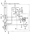
- FIGURE 5 illustrated is a schematic diagram of a switching power supply 500 employing an embodiment of a current mode controller and incorporating an embodiment of an input voltage detection circuit 510 constructed according to the principles of the present invention.
- the switching power supply 500 is analogous to the aforementioned switching power supplies with the exception that the input voltage detection circuit 510 is incorporated to change the level of a sensed inductor current fed back to the current mode controller. The modification of the sensed inductor current is based on the range of an input line voltage.
- the input voltage detection circuit 510 includes a first and second detection resistors 520, 530 that are coupled to a detection filter capacitor 540.
- a sensing resistor 525 is coupled between a rectifier 505 and a converter 507 to sense a converter inductor current.
- the detection filter capacitor 540 used to filter the sensed input voltage, is coupled to a detection switch controller 560.
- the detection switch controller 560 is coupled to a detection switch 580 (e.g. , transistor) that is coupled to a third and fourth gain controlling resistors 550, 570.
- the third and fourth gain controlling resistors 550, 570 are coupled to a summing node 555.
- the summing node 555 is coupled to the inverting input of a comparator op-amp 549 and a ramp generator 550.
- the sensed input line voltage is provided to the detection switch controller 560 that determines whether the detection switch 580 is turned ON or OFF.
- the detection switch 580 is used to configure the resistive path of the sensed inductor current to the comparator op-amp 549.
- the detection switch controller 560 decides the signal path based on the value of the input line voltage, resulting in a low input line or high input line voltage mode of operation.
- the third and fourth gain controlling resistors 550, 570 accordingly modifies the sensed inductor current signal. By selectively using a different resistive value based on the input line voltage to change the level of the sensed inductor current, the THD over the entire input line voltage range can be minimized.
- FIGURE 6 illustrated is a schematic diagram of a switching power supply 600 employing an embodiment of a current mode controller 640 with low/high line detection constructed according to the principles of the present invention.
- the switching power supply 600 includes a rectifier 610 that is coupled to a converter 620.
- the converter 620 is coupled to a output capacitor 615, sensing resistor 630 and a converter inductor 625.
- a current mode controller 640 with low/high line detection that is coupled to the rectifier 610, converter 620, output capacitor 615, sensing resistor 630 and converter inductor 625.
- the current mode controller 640 with low/high line detection includes a first and second resistor 641, 642 that make up a voltage divider circuit.
- a third resistor 643 is coupled to the first and second resistors 641, 642 and to an inverting input of a voltage-loop error operational amplifier (op-amp) 646.
- An integrating capacitor 645 is coupled (in a feedback path) between the inverting input and the output of the voltage-loop error op-amp 646.
- the non-inverting input of the voltage-loop error op-amp 646 is coupled to a first reference voltage 644.
- the output of the voltage-loop error op-amp 646 is coupled to a fourth resistor 647 that is coupled to a fifth resistor 648 and to the non-inverting input of a second op-amp 649.
- a sixth resistor 650 is coupled to the output and to the inverting input of the second op-amp 649.
- a compensating resistor 651 is coupled to the converter inductor 625 and to the inverting input of the second op-amp 649.
- the output of the second op-amp 649 is also coupled to the non-inverting input of a comparator op-amp 652.
- the comparator op-amp 652 inverting input is coupled to a summing node 653.
- the summing node 653 is coupled to a seventh and eight resistors 657, 658, respectively, and to a ramp waveform generator 654.
- the seventh and eight resistors 657, 658 are coupled to the sensing resistor 630 and to a switch 659, which is typically a transistor.
- the switch 659 is controlled by a switching op-amp 655, which has its non-inverting input coupled to the output of the voltage-loop error op-amp 646 and its inverting input coupled to a second reference voltage 656.
- the converter's switch (not shown) duty cycle which is primarily independent of the output power, is primarily determined by the input line voltage.
- the converter's switch duty cycle is smaller at a high input line voltage and conversely, the converter's switch duty cycle is larger at a low input line voltage.
- the output of the voltage-loop error op-amp 646 may be used to detect the input line voltage range. A high output from the voltage-loop error op-amp 646 indicates a low input line voltage, while a low output from the voltage-loop error op-amp 646 indicates a high input line voltage.
- the output from the voltage-loop error op-amp 646 is compared to the second reference voltage 656 at the switching op-amp 655, which determines the switch 659 operation.
- different resistive paths for high or low line operation
- the sensed inductor current to the summing node 653.
- the output of the voltage-feedback op-amp 148 illustrated in FIGURE 1 may also be used to determine the input line voltage range information.
- the voltage-feedback op-amp 148 output peak value is an indication of the input line voltage range. It should be noted that the converter's switch duty cycle does not correctly reflect the input line voltage at DCM during light load operations. However, since higher THD may be tolerated at light load conditions, the converter is still able to meet the power quality standards of IEC-1000.3.2.
- the THD can be further improved by continuously adjusting the amplitude of the ramp signal according to the rectified line voltage.
- the input current THD can maintained at a value substantially lower than 10% over the entire range of the input line voltage with an optimum ramp injection.
- FIGURE 7A illustrated is an optimum ramp injection as a function of the root-mean-square (rms) input line voltage.
- a digital or analog function generator may be used to generate a current or voltage proportional to the optimum ramp. The current or voltage generated is then used to control the charging of a RC circuit that produces the desired ramp. It is also possible to approximate the optimum ramp with two simple functions as depicted in FIGUREs 7B and 7C.
- FIGURE 7B illustrated is a two-level approximation of an optimum ramp injection as a function of the input line voltage.
- the two levels illustrate a low line operation and a high line operation.
- the result of the approximation is similar to the changing current sensing method described above.
- FIGURE 7C illustrated is a two-line approximation of an optimum ramp injection as a function of the line voltage.
- the piece-wise linear curve depicted in FIGURE 6C may be produced by an op-amp with diodes in the op-amp's feedback path.
- the input to the op-amp is the rms input line voltage signal that is generally obtained by filtering the rectified input voltage.
- the present invention provides, for use with a power factor correction circuit, a current mode controller, a method of operating a power factor correction circuit to achieve current mode control thereof and a power supply incorporating the controller or the method.
- the controller includes: (1) a modulator, coupled to a switch in the power factor correction circuit, that senses an electrical characteristic and a current passing through the power factor correction circuit and provides, in response thereto, a control signal to the switch and (2) a compensation circuit, coupled to an input of the power factor correction circuit, that provides a compensation signal to the modulator that is a function of a rectified line voltage provided to the input of the power factor correction circuit, the compensation signal causing the modulator to modify the control signal to reduce a THD of the power factor correction circuit.
Landscapes
- Engineering & Computer Science (AREA)
- Power Engineering (AREA)
- Dc-Dc Converters (AREA)
- Rectifiers (AREA)
- Control Of Electrical Variables (AREA)
Applications Claiming Priority (2)
| Application Number | Priority Date | Filing Date | Title |
|---|---|---|---|
| US905105 | 1997-08-01 | ||
| US08/905,105 US5912549A (en) | 1997-08-01 | 1997-08-01 | Current mode controller for continuous conduction mode power factor correction circuit and method of operation thereof |
Publications (2)
| Publication Number | Publication Date |
|---|---|
| EP0895339A2 true EP0895339A2 (de) | 1999-02-03 |
| EP0895339A3 EP0895339A3 (de) | 2000-11-08 |
Family
ID=25420300
Family Applications (1)
| Application Number | Title | Priority Date | Filing Date |
|---|---|---|---|
| EP98306014A Withdrawn EP0895339A3 (de) | 1997-08-01 | 1998-07-28 | Stromartsteuereinrichtung und Betriebsverfahren für Leistungsfaktorkorrekturschaltung mit ständig leitendem Modus |
Country Status (3)
| Country | Link |
|---|---|
| US (1) | US5912549A (de) |
| EP (1) | EP0895339A3 (de) |
| CA (1) | CA2244044C (de) |
Cited By (11)
| Publication number | Priority date | Publication date | Assignee | Title |
|---|---|---|---|---|
| DE19854567A1 (de) * | 1998-11-26 | 2000-06-08 | Danfoss Compressors Gmbh | Verfahren zum Steuern einer Gleichrichterschaltung und Gleichrichterschaltung |
| WO2002021671A1 (en) * | 2000-09-05 | 2002-03-14 | Minebea Co. Ltd. | Active power factor correction |
| US6445600B2 (en) | 1998-07-13 | 2002-09-03 | Ben-Gurion University Of The Negev Research & Development Authority | Modular structure of an apparatus for regulating the harmonics of current drawn from power lines by an electronic load |
| US6781352B2 (en) | 2002-12-16 | 2004-08-24 | International Rectifer Corporation | One cycle control continuous conduction mode PFC boost converter integrated circuit with integrated power switch and boost converter |
| DE102005050337A1 (de) * | 2005-10-20 | 2007-04-26 | Siemens Ag | Gleichstromsteller und Verfahren zum Betreiben eines Gleichstromstellers |
| CN102497700A (zh) * | 2011-12-05 | 2012-06-13 | 北方工业大学 | 一种用于led照明的功率因数校正方法 |
| CN102497701A (zh) * | 2011-12-05 | 2012-06-13 | 北方工业大学 | 一种用于降低led驱动电路谐波失真的功率因数校正电路 |
| CN102738797A (zh) * | 2012-05-31 | 2012-10-17 | 江苏盈方智能科技有限公司 | 用于智能滤波装置的数字信号处理器双dsp电路 |
| NL2007910A (en) * | 2011-08-17 | 2013-02-19 | Google Inc | Power factor correction circuitry and methodology to compensate for leading power factor. |
| CN103178582A (zh) * | 2013-03-12 | 2013-06-26 | 广东易事特电源股份有限公司 | 一种具有功率因数校正功能的工频在线式不间断电源 |
| EP2953252A3 (de) * | 2014-06-05 | 2016-04-27 | Hamilton Sundstrand Corporation | Systeme und verfahren zur steuerung aktiver gleichrichter |
Families Citing this family (46)
| Publication number | Priority date | Publication date | Assignee | Title |
|---|---|---|---|---|
| DE10032846A1 (de) * | 1999-07-12 | 2001-01-25 | Int Rectifier Corp | Leistungsfaktor-Korrektursteuerschaltung |
| US6359426B1 (en) * | 1999-11-24 | 2002-03-19 | Enterasys Networks, Inc. | Voltage threshold circuit for power conditioner |
| US6388429B1 (en) * | 2000-03-09 | 2002-05-14 | Hengchun Mao | Controller for power factor corrector and method of operation thereof |
| US6411530B2 (en) * | 2000-04-06 | 2002-06-25 | Robicon Corporation | Drive and power supply with phase shifted carriers |
| US7564220B2 (en) * | 2000-09-21 | 2009-07-21 | O2Micro International Ltd. | Method and electronic circuit for efficient battery wake up charging |
| US7348760B2 (en) | 2000-09-21 | 2008-03-25 | O2Micro International Limited | Power management topologies |
| US6590439B1 (en) * | 2000-10-13 | 2003-07-08 | Maxim Integrated Products, Inc. | High voltage integrated Miller capacitor feedback circuit |
| JP2002223132A (ja) * | 2001-01-29 | 2002-08-09 | Niigata Seimitsu Kk | 音声再生装置および方法 |
| US6465990B2 (en) | 2001-03-15 | 2002-10-15 | Bensys Corporation | Power factor correction circuit |
| US6492794B2 (en) | 2001-03-30 | 2002-12-10 | Champion Microelectronic Corp. | Technique for limiting current through a reactive element in a voltage converter |
| US6531854B2 (en) * | 2001-03-30 | 2003-03-11 | Champion Microelectronic Corp. | Power factor correction circuit arrangement |
| JP3689645B2 (ja) * | 2001-05-21 | 2005-08-31 | 松下電器産業株式会社 | データ幅補正装置 |
| WO2003001315A1 (en) | 2001-06-21 | 2003-01-03 | Champion Microelectronic Corp. | Volt-second balanced pfc-pwm power converter |
| US7064521B2 (en) * | 2001-08-17 | 2006-06-20 | O2Micro International Limited | Charging circuit for parallel charging in multiple battery systems |
| US7202634B2 (en) * | 2001-08-17 | 2007-04-10 | O2Micro International Limited | Voltage mode, high accuracy battery charger |
| US6498461B1 (en) | 2001-08-17 | 2002-12-24 | O2 Micro International Limited | Voltage mode, high accuracy battery charger |
| US6664774B2 (en) | 2002-03-27 | 2003-12-16 | Semtech Corporation | Offset peak current mode control circuit for multiple-phase power converter |
| US7118793B2 (en) * | 2002-05-22 | 2006-10-10 | Swei Mu Wang | Three-dimensional foamable structure with wear-resistant feature |
| US6768658B2 (en) | 2002-09-04 | 2004-07-27 | Artesyn Technologies, Inc. | DC-DC power supply with at least two paralleled converters and current share method for same |
| US6879134B2 (en) * | 2003-02-11 | 2005-04-12 | O2Micro International Limited | Selector circuit for power management in multiple battery systems |
| US20040174152A1 (en) * | 2003-03-04 | 2004-09-09 | Hwang Jeffrey H. | Pulse-skipping switching power converter |
| TWI292248B (en) * | 2003-05-01 | 2008-01-01 | Delta Electronics Inc | Alternative control method for application to boost converter |
| US6828759B1 (en) * | 2003-05-15 | 2004-12-07 | Motorola, Inc. | Circuit for regulating current to multiple batteries in a battery charger |
| US7433211B1 (en) | 2003-06-30 | 2008-10-07 | Iwatt Inc. | System and method for input current shaping in a power converter |
| WO2005041393A2 (en) | 2003-10-24 | 2005-05-06 | Pf1, Inc. | Method and system for power factor correction |
| TWI255088B (en) * | 2004-05-24 | 2006-05-11 | Anpec Electronics Corp | DC converting controller with mode-switching and over-current protection by using multifunctional pin and its method |
| US7317625B2 (en) * | 2004-06-04 | 2008-01-08 | Iwatt Inc. | Parallel current mode control using a direct duty cycle algorithm with low computational requirements to perform power factor correction |
| US7095217B1 (en) | 2005-03-31 | 2006-08-22 | O2Micro International Limited | Method circuitry and electronic device for controlling a variable output dc power source |
| US7268520B2 (en) * | 2005-04-08 | 2007-09-11 | O2Micro International Limited | Sense amplifier for use with wake-up charging current |
| CN100527580C (zh) * | 2006-01-23 | 2009-08-12 | 崇贸科技股份有限公司 | 利用前馈电压补偿的电源转换装置及其方法 |
| US7868603B2 (en) * | 2006-10-04 | 2011-01-11 | Microsemi Corporation | Method and apparatus to compensate for supply voltage variations in a PWM-based voltage regulator |
| MY158596A (en) * | 2007-01-15 | 2016-10-31 | Oyl Res And Dev Ct Sdn Bhd | A power factor correction circuit |
| US7800351B2 (en) * | 2008-03-24 | 2010-09-21 | Active-Semi, Inc. | High efficiency voltage regulator with auto power-save mode |
| US8614595B2 (en) * | 2008-11-14 | 2013-12-24 | Beniamin Acatrinei | Low cost ultra versatile mixed signal controller circuit |
| US8934266B2 (en) * | 2011-08-26 | 2015-01-13 | System General Corp. | Adaptive slope compensation programmable by input voltage of power converter |
| US20130207632A1 (en) * | 2012-02-13 | 2013-08-15 | Gurjit Singh THANDI | System and method for improved line transient response in current mode boost converters |
| CN103368372B (zh) * | 2012-04-06 | 2016-04-20 | 英飞特电子(杭州)股份有限公司 | 功率因数校正电路 |
| US9578692B2 (en) | 2012-04-19 | 2017-02-21 | Infineon Technologies Americas Corp. | Power converter with tank circuit and over-voltage protection |
| WO2014009773A1 (en) * | 2012-07-11 | 2014-01-16 | Roal Electronics S.P.A. | Control circuit for reducing of total harmonic distortion (thd) in the power supply to an electric load |
| US20140225530A1 (en) * | 2013-02-09 | 2014-08-14 | Power metrics International | Dynamic Means for Correcting for Load Imbalance and Harmonic Distortion |
| US20150200604A1 (en) * | 2013-10-10 | 2015-07-16 | Robert Turner | Dynamic Means for Correcting for Load Imbalance and Harmonic Distortion |
| EP2887275A1 (de) * | 2013-12-20 | 2015-06-24 | BASF Coatings GmbH | Verfahren und System zur Bestimmung einer Farbformel |
| JP6489030B2 (ja) * | 2016-01-22 | 2019-03-27 | 株式会社デンソー | 昇圧電源装置 |
| CN106787675B (zh) * | 2016-12-28 | 2019-04-23 | 成都芯源系统有限公司 | 具有功率因数校正功能的谐振变换器及其控制器 |
| TWI704757B (zh) * | 2020-02-11 | 2020-09-11 | 宏碁股份有限公司 | 升壓轉換器 |
| CN119210133B (zh) * | 2024-10-15 | 2026-02-13 | 珠海格力电器股份有限公司 | 一种电路和电路的功率处理方法和空调 |
Family Cites Families (5)
| Publication number | Priority date | Publication date | Assignee | Title |
|---|---|---|---|---|
| US4119907A (en) * | 1977-05-27 | 1978-10-10 | Xerox Corporation | Power factor corrector for a resistive load |
| US5600459A (en) * | 1993-12-20 | 1997-02-04 | Roy; Howard S. | Multiple-shutter flat-panel display having individually controlled pixels and method for making same |
| US5734562A (en) * | 1994-06-20 | 1998-03-31 | Redl; Richard | Power factor correction circuit |
| US5568041A (en) * | 1995-02-09 | 1996-10-22 | Magnetek, Inc. | Low-cost power factor correction circuit and method for electronic ballasts |
| ES2150072T3 (es) * | 1995-05-26 | 2000-11-16 | At & T Corp | Control del factor de potencia en rectificadores conmutados. |
-
1997
- 1997-08-01 US US08/905,105 patent/US5912549A/en not_active Expired - Fee Related
-
1998
- 1998-07-28 EP EP98306014A patent/EP0895339A3/de not_active Withdrawn
- 1998-07-28 CA CA002244044A patent/CA2244044C/en not_active Expired - Fee Related
Cited By (13)
| Publication number | Priority date | Publication date | Assignee | Title |
|---|---|---|---|---|
| US6445600B2 (en) | 1998-07-13 | 2002-09-03 | Ben-Gurion University Of The Negev Research & Development Authority | Modular structure of an apparatus for regulating the harmonics of current drawn from power lines by an electronic load |
| DE19854567A1 (de) * | 1998-11-26 | 2000-06-08 | Danfoss Compressors Gmbh | Verfahren zum Steuern einer Gleichrichterschaltung und Gleichrichterschaltung |
| WO2002021671A1 (en) * | 2000-09-05 | 2002-03-14 | Minebea Co. Ltd. | Active power factor correction |
| US6781352B2 (en) | 2002-12-16 | 2004-08-24 | International Rectifer Corporation | One cycle control continuous conduction mode PFC boost converter integrated circuit with integrated power switch and boost converter |
| DE102005050337A1 (de) * | 2005-10-20 | 2007-04-26 | Siemens Ag | Gleichstromsteller und Verfahren zum Betreiben eines Gleichstromstellers |
| NL2007910A (en) * | 2011-08-17 | 2013-02-19 | Google Inc | Power factor correction circuitry and methodology to compensate for leading power factor. |
| CN102497701A (zh) * | 2011-12-05 | 2012-06-13 | 北方工业大学 | 一种用于降低led驱动电路谐波失真的功率因数校正电路 |
| CN102497700A (zh) * | 2011-12-05 | 2012-06-13 | 北方工业大学 | 一种用于led照明的功率因数校正方法 |
| CN102738797A (zh) * | 2012-05-31 | 2012-10-17 | 江苏盈方智能科技有限公司 | 用于智能滤波装置的数字信号处理器双dsp电路 |
| CN103178582A (zh) * | 2013-03-12 | 2013-06-26 | 广东易事特电源股份有限公司 | 一种具有功率因数校正功能的工频在线式不间断电源 |
| CN103178582B (zh) * | 2013-03-12 | 2016-02-03 | 广东易事特电源股份有限公司 | 一种具有功率因数校正功能的工频在线式不间断电源 |
| EP2953252A3 (de) * | 2014-06-05 | 2016-04-27 | Hamilton Sundstrand Corporation | Systeme und verfahren zur steuerung aktiver gleichrichter |
| US9473040B2 (en) | 2014-06-05 | 2016-10-18 | Hamilton Sundstrand Corporation | Systems and methods for controlling active rectifiers |
Also Published As
| Publication number | Publication date |
|---|---|
| US5912549A (en) | 1999-06-15 |
| CA2244044C (en) | 2001-06-05 |
| CA2244044A1 (en) | 1999-02-01 |
| EP0895339A3 (de) | 2000-11-08 |
Similar Documents
| Publication | Publication Date | Title |
|---|---|---|
| US5912549A (en) | Current mode controller for continuous conduction mode power factor correction circuit and method of operation thereof | |
| US5349284A (en) | Power factor boost converter power supply | |
| US6882551B2 (en) | Switching power supply device | |
| US6388429B1 (en) | Controller for power factor corrector and method of operation thereof | |
| US5602463A (en) | DC power supply with enhanced input power factor using a buck and boost converter | |
| US6191565B1 (en) | Power factor compensation controller | |
| US4942509A (en) | Control arrangement for a switch mode power supply | |
| US6946819B2 (en) | Device for the correction of the power factor in power supply units with forced switching operating in transition mode | |
| US6437994B1 (en) | LLC converter includes a current variation detector for correcting a frequency adjusting control signal of an included difference detector | |
| US4672518A (en) | Current mode control arrangement with load dependent ramp signal added to sensed current waveform | |
| KR100206143B1 (ko) | 고역률 보상회로 | |
| US6034513A (en) | System and method for controlling power factor and power converter employing the same | |
| US5644214A (en) | Power factor correction circuit | |
| EP2187512B1 (de) | Verfahren und Vorrichtung zur Steuerung einer Leistungsfaktorverbesserungsschaltung | |
| US5982639A (en) | Two switch off-line switching converter | |
| WO2002079892B1 (en) | Power factor correction circuit arrangement | |
| US6141232A (en) | Fixed frequency flyback converter | |
| US6115274A (en) | Frequency modulation controller for single-switch, polyphase, DCM boost converter and method of operation thereof | |
| US8289738B2 (en) | Switching power supply | |
| EP1580639B1 (de) | Übergangsmodus-Leistungsfaktorkorrekturvorrichtung in Schaltnetzteilen | |
| KR20080086798A (ko) | 고전압 전력 공급 회로용 방법 및 장치 | |
| JP3472517B2 (ja) | 直流安定化電源装置 | |
| JP7640492B2 (ja) | スイッチング電源装置 | |
| US6177784B1 (en) | Large signal gain modifier circuit | |
| JPH05219736A (ja) | スイッチング電源装置 |
Legal Events
| Date | Code | Title | Description |
|---|---|---|---|
| PUAI | Public reference made under article 153(3) epc to a published international application that has entered the european phase |
Free format text: ORIGINAL CODE: 0009012 |
|
| AK | Designated contracting states |
Kind code of ref document: A2 Designated state(s): AT BE CH CY DE DK ES FI FR GB GR IE IT LI LU MC NL PT SE |
|
| AX | Request for extension of the european patent |
Free format text: AL;LT;LV;MK;RO;SI |
|
| PUAL | Search report despatched |
Free format text: ORIGINAL CODE: 0009013 |
|
| AK | Designated contracting states |
Kind code of ref document: A3 Designated state(s): AT BE CH CY DE DK ES FI FR GB GR IE IT LI LU MC NL PT SE |
|
| AX | Request for extension of the european patent |
Free format text: AL;LT;LV;MK;RO;SI |
|
| AKX | Designation fees paid | ||
| REG | Reference to a national code |
Ref country code: DE Ref legal event code: 8566 |
|
| STAA | Information on the status of an ep patent application or granted ep patent |
Free format text: STATUS: THE APPLICATION IS DEEMED TO BE WITHDRAWN |
|
| 18D | Application deemed to be withdrawn |
Effective date: 20010509 |