EP0896372A2 - Solarbatteriemodul - Google Patents
Solarbatteriemodul Download PDFInfo
- Publication number
- EP0896372A2 EP0896372A2 EP98306313A EP98306313A EP0896372A2 EP 0896372 A2 EP0896372 A2 EP 0896372A2 EP 98306313 A EP98306313 A EP 98306313A EP 98306313 A EP98306313 A EP 98306313A EP 0896372 A2 EP0896372 A2 EP 0896372A2
- Authority
- EP
- European Patent Office
- Prior art keywords
- layer
- solar battery
- battery module
- surface material
- photocatalyst
- Prior art date
- Legal status (The legal status is an assumption and is not a legal conclusion. Google has not performed a legal analysis and makes no representation as to the accuracy of the status listed.)
- Granted
Links
Images


Classifications
-
- H—ELECTRICITY
- H02—GENERATION; CONVERSION OR DISTRIBUTION OF ELECTRIC POWER
- H02S—GENERATION OF ELECTRIC POWER BY CONVERSION OF INFRARED RADIATION, VISIBLE LIGHT OR ULTRAVIOLET LIGHT, e.g. USING PHOTOVOLTAIC [PV] MODULES
- H02S40/00—Components or accessories in combination with PV modules, not provided for in groups H02S10/00 - H02S30/00
- H02S40/10—Cleaning arrangements
-
- H—ELECTRICITY
- H10—SEMICONDUCTOR DEVICES; ELECTRIC SOLID-STATE DEVICES NOT OTHERWISE PROVIDED FOR
- H10F—INORGANIC SEMICONDUCTOR DEVICES SENSITIVE TO INFRARED RADIATION, LIGHT, ELECTROMAGNETIC RADIATION OF SHORTER WAVELENGTH OR CORPUSCULAR RADIATION
- H10F19/00—Integrated devices, or assemblies of multiple devices, comprising at least one photovoltaic cell covered by group H10F10/00, e.g. photovoltaic modules
- H10F19/80—Encapsulations or containers for integrated devices, or assemblies of multiple devices, having photovoltaic cells
-
- Y—GENERAL TAGGING OF NEW TECHNOLOGICAL DEVELOPMENTS; GENERAL TAGGING OF CROSS-SECTIONAL TECHNOLOGIES SPANNING OVER SEVERAL SECTIONS OF THE IPC; TECHNICAL SUBJECTS COVERED BY FORMER USPC CROSS-REFERENCE ART COLLECTIONS [XRACs] AND DIGESTS
- Y02—TECHNOLOGIES OR APPLICATIONS FOR MITIGATION OR ADAPTATION AGAINST CLIMATE CHANGE
- Y02E—REDUCTION OF GREENHOUSE GAS [GHG] EMISSIONS, RELATED TO ENERGY GENERATION, TRANSMISSION OR DISTRIBUTION
- Y02E10/00—Energy generation through renewable energy sources
- Y02E10/50—Photovoltaic [PV] energy
Definitions
- the present invention relates to a solar battery, and particularly to a solar battery module exhibiting an effect of preventing contamination to a surface material thereby preventing loss of irradiation energy of solar light to a solar battery.
- a solar battery module of a crystal system (using a single crystal or polycrystalline silicon wafer) has a configuration, for example, shown in Fig. 1 in which a surface layer 22 is laminated by way of an adhesive layer 21 to the front surface of a solar battery cell 20, and an underlying film 24 is laminated by way of an adhesive layer 23 on the back surface.
- the surface material which is mainly composed of a fluororesin film, has a problem that it is contaminated during long time use to cause a considerably loss of irradiation energy of the sunlight to the solar battery.
- a film of amorphous silicon is usually formed on a glass substrate used as a surface material to constitute a module structure, which also results in contamination to the surface material.
- An object of the present invention is to provide a solar battery module capable of preventing contamination to a surface material as much as possible thereby maintaining a high electric generation power over a long period of time.
- a solar battery module including: a solar battery cell; and a surface material laminated to cover a surface of said cell; wherein a photocatalyst layer is formed on said surface material.
- the above photocatalyst layer is formed on said surface material directly or by way of an underlying layer.
- the above module further includes a photocatalyst film in which a photocatalyst layer is formed on one surface of a substrate directly or by way of an underlaying layer, and a pressure sensitive adhesive layer is formed on the other surface of said substrate; wherein said pressure sensitive adhesive layer is stuck on said surface material, to form a photocatalyst layer on said surface material.
- the above photocatalyst layer includes a metal oxide layer obtained by disposing a substrate on the side of a sputtering space between targets facing to each other, and forming a sputter layer on said substrate by reactive sputtering in an inert gas containing an oxygen molecule-containing gas using an facing target sputtering apparatus.
- the corresponding method is an independent aspect of the teachings herein.
- the photocatalyst layer is a titanium oxide layer.
- the photocatalyst layer made of titanium oxide or the like is formed on the surface material, even when contaminates such as dusts or finger prints are deposited to the photocatalyst layer on the surface, the photocatalyst is excited by photoirradiation by a light, for example, from the solar battery cell, the various contaminates deposited to the photocatalyst layer on the surface are decomposed and eliminated to reduce or prevent contamination as much as possible.
- the photocatalyst layer can be formed, for example, by a sputtering process.
- a photocatalyst layer of metal e.g. T; oxide film by an opposed target type sputtering process and preferably to conduct sputtering with a volume ratio between an inert gas and an oxygen gas from an oxygen molecule-containing gas at 2:1 to 1:3 and, more preferably, by increasing the power applied to the target.
- the opposed target type sputtering process has been known, for example, by Japanese Patent Publication Nos. Sho 62-56575, Sho 63-20304 and Hei 3-1810, in which perpendicular magnetic recording thin films and the like are formed by the opposed target type sputtering process. Then, it is described that films of good crystallinity can be formed by this method.
- films of good crystallinity can be formed by this method.
- the photocatalytical effect is lower when most of crystal systems obtained are of rutile type.
- an anatase rich photocatalyst layer can be prepared at a low temperature and, particularly, a photocatalyst layer enriched more with the anatase type crystals can be formed by adjusting the ratio between inert e.g. argon gas and an oxygen gas to the above ratio, and the layer quality can be coarsened to enlarge the surface area by increasing the power applied, so that catalytical activity can be more increased.
- inert e.g. argon gas and an oxygen gas
- a solar battery module has such a configuration as shown in Fig. 1 in which a photocatalyst layer is formed on a surface material 22 to a thickness of 0.001 to 10 ⁇ m, preferably, 0.01 to 1 ⁇ m.
- the photocatalyst layer may be formed on the surface material directly or, preferably, by way of an underlying film.
- a photocatalyst film 10 shown in Fig. 2 may be stuck on the surface material.
- the photocatalyst film 10 is configured such that a photocatalyst layer 13 is formed by way of an underlying layer 12 on one surface of a substrate 11; an adhesive layer 14 is formed on the other surface of the substrate 11; and, if necessary, a releasing film 15 is releasably stuck on the adhesive layer 14.
- the photocatalyst film 10 is preferably formed to be transparent entirely except for the releasing film 15.
- the substrate there is preferably used a transparent plastic film made from polyester, acrylic resin, cellulose or polycarbonate.
- the thickness is usually, although not necessarily in a range of 10 to 300 ⁇ m, preferably, 20 to 100 ⁇ m.
- the underlying or protective layer may be omitted but is preferably formed if a plastic film is used as the substrate for preventing degradation of the substrate.
- the underlying layer is suitably made from a transparent oxide not having a photocatalyst activity such as SiO 2 , Al 2 O 3 or ITO, and a transparent material less photodegradable such as a sulfide, nitride, boride or carbide of a metal.
- the thickness of the underlying layer may be suitably selected, and is usually in a range of 10 to 5 ⁇ m, preferably, 20 to 1 ⁇ m.
- the underlying layer can be formed by a sputtering process, vapor-phase plating process such as vacuum-deposition, or other appropriate means.
- the adhesive layer can be formed of a known acrylic or epoxy type pressure sensitive adhesive, or heat or light crosslinked pressure sensitive adhesive formed by adding an organic peroxide or a photoinitiator to an ethylene-vinyl acetate copolymer.
- the thickness is usually in a range of 1 to 500 ⁇ m, preferably, 5 to 100 ⁇ m.
- any known type can be used.
- the photocatalyst film 10 is used by removing the releasing film 15 and sticking the pressure sensitive adhesive layer 14 on the surface material of the solar battery module.
- the kind, thickness and the formation method of the underlying layer through which the photocatalyst layer is formed on the surface material, are the same as described above.
- the photocatalyst layer can be made from an oxide of a metal having a photocatalytic activity such as titanium, zinc, tungsten or iron. While not exclusively, the photocatalyst layer is preferably formed by reactive sputtering in an inert gas containing an oxygen molecule-containing gas using a metal target.
- the sputtering can be conducted by a known process, for example, a usual magnetron sputtering process, and preferably by a facing target sputtering apparatus.
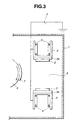
- FIG. 3 As a facing target sputtering apparatus, there can be used a known system typically shown in Fig. 3.
- reference numeral 1 denotes a system main body the inside of which can be degassed and evacuated.
- a pair of metal targets 2, spaced at a specific gap, are oppositely disposed in the system main body 1.
- the targets 2 are held on holders 3 having supports 3 a respectively, and connected by way of the holders 3 to the cathodes of a DC power source (sputtering power source).
- Magnets 5 are disposed at the back of the targets 2 such that different magnetic poles are opposed so as to generate magnetic fields in the direction perpendicular to the targets 2 in a sputtering space 6 between the targets 2.
- a substrate 7 on which a sputter film is to be formed is disposed on the side of the sputtering space 6.
- Reference numeral 8 denotes a supporting member 8 for supporting the substrate 7 movably in a predetermined direction.
- a metal oxide MeOx having a photocatalytical activity (Me represents a metal such as Al, Co, Cu, Fe, In, Mg, Sn, Ti or Zn and x is a positive number within a range of 0 to 10, preferably, 0 to 5 while varying depending on the kind of the metal, but x is not always necessary to correspond to the valence number of the metal).
- MeOx represents a metal such as Al, Co, Cu, Fe, In, Mg, Sn, Ti or Zn
- x is a positive number within a range of 0 to 10, preferably, 0 to 5 while varying depending on the kind of the metal, but x is not always necessary to correspond to the valence number of the metal.
- titanium forming a titanium oxide film is preferably used as the above metal Me.
- an inert gas and oxygen molecule-containing gas are introduced after the vacuum degree is set at a value of 0.1 to 100 mTorr, particularly, 1 to 30 mTorr.
- a known gas can be used as an oxygen molecule-containing gas supplied to the sputtering space (oxidative gas). Specifically, oxygen, ozone, air or water can be used, and oxygen is usually used. Further, helium, argon or the like can be used as the inert gas and, particularly, argon which is industrially inexpensive can be suitably used.
- the inert gas and the oxygen molecule-containing gas are preferably introduced at a ratio of the inert gas and the oxygen gas of 2:1 to 1:3, particularly, 1.5:1 to 1:2 (by volume ratio).
- a ratio of the inert gas and the oxygen gas of 2:1 to 1:3, particularly, 1.5:1 to 1:2 (by volume ratio).
- the flow rate of the gas is suitably selected depending on the size of the chamber and the number of cathodes, usually in a range of about 2 to 1000 cc/min as the total amount of the inert gas and the oxygen molecule-containing gas.
- the electric power applied is suitably selected, and is preferably set at a high value.
- the amount of energy per target area is 1.3 W/cm 2 or more, preferably, 2.6 W/cm 2 or more and, more preferably, 5.1 W/cm 2 or more. Since the film quality of the photocatalyst layer thus formed can be coarsened and the surface area can be increased, the performance of the photocatalyst layer can be further improved. If the electric power applied is less than 400 W, and the amount of energy per target area is less than 1.3 W/cm 2 , a photocatalyst layer having a high activity can not be certainly obtained.
- a DC current is used for the power source in the example shown in the figure
- the present invention is not limited thereto.
- a high frequency power source or the like can be used.
- the configuration of the system is also not limited to that in the example shown in the figure.
- the pressure upon sputtering may be set in a range of 1 mTorr to 1 Torr.
- ions of a metal such as platinum, nickel, chromium, cobalt, tin, niobium or tantalum can be ion-implanted in the surface of the metal oxide film at about 1 x 10¹⁵ to 1 x 10¹⁸ ions/cm 2 by a known ion implantation process and system.
- ion-implantation is effective to form a photocatalyst layer having a higher activity.
- photocatalyst layer 13 is prepared, as shown in Fig. 4, by alternately laminating metal oxide films 13a formed as described above and thin films 13b of a metal selected from platinum, nickel, chromium, cobalt, tin, niobium and tantalum or an oxide thereof such that the thin metal oxide film 13a is on the uppermost surface layer and by forming a plurality of holes or grooves 13c of a depth reaching from the uppermost surface layer to the lowermost layer.
- the specific surface area of the photocatalyst layer 13 can be increased and the photocatalyst activity is further increased by the charge separation promoting effect of the photocatalyst of the thin film of metal or oxide thereof.
- the total number of the metal oxide films 13a or the metal or oxide thin films 13b can be set in a range of two to several tens, and the thickness per one layer can be set in a range of 20 to 200, preferably, about 20 to 50.
- the holes or grooves can be formed by laser processing or the like and the shape of them is not limited to a V-shape shown in the figure but can be variously selected. Further, the number of holes or grooves is not limited, and the grooves can be usually formed with a pitch of 0.001 to 5 mm.
- the configuration of the solar battery module according to the present invention can be the same as the known configuration except for formation of the photocatalyst layer as described above on the surface material.
- the constituent materials there can be used known materials.
- a transparent material is mainly used as the surface material because the surface material is required to supply solar light energy efficiently to a battery layer.
- an inorganic material glass
- an organic film such as a polyester film, nylon film or acryl films can be used as the surface material; however, since such a organic film is poor in weather proofness, fluororesin film such as an ETFE or FEP is actually used as the surface material. Since the weather proofness and the like can be improved by formation of the photocatalyst layer on the surface, the above polyester film may be used as the surface material.
- an adhesive for bonding the surface material to the solar battery cell an EVA type adhesive can be used.
- a fluororesin film (ETFE: ethylene-tetrafluoroethylene copolymer) having a width of 300 mm was subjected to corona discharging treatment in a nitrogen atmosphere to activate the surface of the film. Then, the film was placed in a roll coater type sputtering system, which was evacuated by a vacuum pump. The pressure in the chamber was set to 5 mTorr by supplying an argon gas at a flow rate of 50 cc/min and an oxygen gas at a flow rate of 50 cc/min.
- a power at 3 kW was applied from a DC current source to a silicon target by a magnetron sputtering gun, and a silicon oxide film of 50 ⁇ was coated on the ETFE film at a moving rate of 1 m/min. Then, a power of 6 kW was applied by a DC current source to opposed target sputtering cathodes having two titanium targets (100 x 400 mm) attached thereto, and a film was formed at a sheet moving rate of 10 mm/min to form a titanium oxide film of about 2000 ⁇ on the ETFE film.
- a solar battery cell was put between an underlying film (aluminum tedler film) and the above titanium oxide coated fluororesin film as a surface window material using an ethylene-vinyl acetate copolymer type transparent adhesive, followed by lamination by the above adhesive, to prepare a solar battery module shown in Fig. 1.
- the solar battery module was placed in a heavily contaminated outdoor environment and solar light electric generation amount was measured. As a comparison, a solar battery module not coated with any titanium oxide was used. The results are shown in Table 1. In Table 1, numerical values show the ratio of the electric generation amount before and after leaving for one month. Surface Contamination Generation Amount Keeping Rate Comparative Example Dusts are present 0.92 Inventive Example No substantial contamination 0.98
- the module coated with the titanium oxide had no contamination deposition because contaminations on the surface were self-cleaned, and also showed high keeping ratio for the electric generation amount.
- the electric generation amount can be maintained over a long period of time by preventing contamination on the surface material of a solar battery module using a photocatalyst which is photoactivable to decompose environmental surface contaminants, and thereby avoiding loss or irradiation energy of solar light to the solar battery.
Landscapes
- Catalysts (AREA)
- Physical Vapour Deposition (AREA)
- Adhesive Tapes (AREA)
- Adhesives Or Adhesive Processes (AREA)
- Photovoltaic Devices (AREA)
Applications Claiming Priority (3)
| Application Number | Priority Date | Filing Date | Title |
|---|---|---|---|
| JP227603/97 | 1997-08-08 | ||
| JP22760397 | 1997-08-08 | ||
| JP9227603A JPH1168134A (ja) | 1997-08-08 | 1997-08-08 | 太陽電池モジュール |
Publications (3)
| Publication Number | Publication Date |
|---|---|
| EP0896372A2 true EP0896372A2 (de) | 1999-02-10 |
| EP0896372A3 EP0896372A3 (de) | 2000-02-09 |
| EP0896372B1 EP0896372B1 (de) | 2002-11-13 |
Family
ID=16863535
Family Applications (1)
| Application Number | Title | Priority Date | Filing Date |
|---|---|---|---|
| EP98306313A Expired - Lifetime EP0896372B1 (de) | 1997-08-08 | 1998-08-07 | Solarbatteriemodul |
Country Status (4)
| Country | Link |
|---|---|
| US (1) | US6046403A (de) |
| EP (1) | EP0896372B1 (de) |
| JP (1) | JPH1168134A (de) |
| DE (1) | DE69809351T2 (de) |
Cited By (1)
| Publication number | Priority date | Publication date | Assignee | Title |
|---|---|---|---|---|
| EP1475414A1 (de) * | 2003-05-05 | 2004-11-10 | Northrop Grumman Corporation | Selbstdekontaminierender oder selbstreinigender Überzug für Schutz gegen gefährliche Biopathogene und giftige Chemikalien |
Families Citing this family (18)
| Publication number | Priority date | Publication date | Assignee | Title |
|---|---|---|---|---|
| US6599618B1 (en) * | 1999-05-20 | 2003-07-29 | Frederick Lee Simmon, Jr. | Wavelength selective photocatalytic dielectric elements on polytetrafluoroethylene (PTFE) refractors having indices of refraction greater than 2.0 |
| US6335479B1 (en) * | 1998-10-13 | 2002-01-01 | Dai Nippon Printing Co., Ltd. | Protective sheet for solar battery module, method of fabricating the same and solar battery module |
| JP2003527720A (ja) | 1999-10-12 | 2003-09-16 | シーゲイト テクノロジー エルエルシー | ディスクドライブ汚染物減少のための光触媒装置 |
| DE60011544T2 (de) * | 1999-10-28 | 2005-09-15 | Bridgestone Corp. | Verfahren zum Oberflächenbehandeln und Kaschieren eines fluorhaltigen Harzes |
| JP2003062921A (ja) * | 2001-06-11 | 2003-03-05 | Bridgestone Corp | 透明複合フィルム |
| US6911593B2 (en) * | 2002-09-24 | 2005-06-28 | Board Of Trustees Of The University Of Arkansas | Transparent self-cleaning dust shield |
| JP4157459B2 (ja) * | 2003-10-30 | 2008-10-01 | シャープ株式会社 | 軽量太陽電池モジュールとその製造方法 |
| ATE377580T1 (de) | 2004-07-12 | 2007-11-15 | Cardinal Cg Co | Wartungsarme beschichtungen |
| US20070227579A1 (en) * | 2006-03-30 | 2007-10-04 | Benyamin Buller | Assemblies of cylindrical solar units with internal spacing |
| US20080011599A1 (en) | 2006-07-12 | 2008-01-17 | Brabender Dennis M | Sputtering apparatus including novel target mounting and/or control |
| AT504568B1 (de) * | 2006-12-05 | 2010-03-15 | Nanoident Technologies Ag | Schichtaufbau |
| WO2008099975A1 (en) * | 2007-02-13 | 2008-08-21 | Bong Gi Kim | Laminated board generating electricity by sunshine |
| TW200844320A (en) * | 2007-05-08 | 2008-11-16 | Univ Nat Taiwan Science Tech | Window unit and window structure and profound wallboard |
| CA2664369A1 (en) | 2007-09-14 | 2009-03-19 | Cardinal Cg Company | Low-maintenance coatings, and methods for producing low-maintenance coatings |
| JPWO2011059101A1 (ja) * | 2009-11-16 | 2013-04-04 | タムネットワーク株式会社 | 光触媒コーティング |
| JP5919259B2 (ja) * | 2011-03-31 | 2016-05-18 | 三菱樹脂株式会社 | ガスバリア積層フィルムとその製造方法 |
| US8610280B2 (en) | 2011-09-16 | 2013-12-17 | Micron Technology, Inc. | Platinum-containing constructions, and methods of forming platinum-containing constructions |
| US10604442B2 (en) | 2016-11-17 | 2020-03-31 | Cardinal Cg Company | Static-dissipative coating technology |
Family Cites Families (19)
| Publication number | Priority date | Publication date | Assignee | Title |
|---|---|---|---|---|
| JPS57100627A (en) * | 1980-12-12 | 1982-06-22 | Teijin Ltd | Manufacture of vertical magnetic recording medium |
| JPS5818972A (ja) * | 1981-07-27 | 1983-02-03 | Semiconductor Energy Lab Co Ltd | 光電変換装置 |
| US4544470A (en) * | 1984-05-31 | 1985-10-01 | Ford Motor Company | Electrochemical photocatalytic structure |
| US4636578A (en) * | 1985-04-11 | 1987-01-13 | Atlantic Richfield Company | Photocell assembly |
| US4663829A (en) * | 1985-10-11 | 1987-05-12 | Energy Conversion Devices, Inc. | Process and apparatus for continuous production of lightweight arrays of photovoltaic cells |
| US5501744A (en) * | 1992-01-13 | 1996-03-26 | Photon Energy, Inc. | Photovoltaic cell having a p-type polycrystalline layer with large crystals |
| US5476553A (en) * | 1994-02-18 | 1995-12-19 | Ase Americas, Inc. | Solar cell modules and method of making same |
| JP3648756B2 (ja) * | 1994-03-22 | 2005-05-18 | Jsr株式会社 | 半導体素子用コーテイング材 |
| JP2756082B2 (ja) * | 1994-04-28 | 1998-05-25 | キヤノン株式会社 | 太陽電池モジュールの製造方法 |
| JP3333892B2 (ja) * | 1994-09-05 | 2002-10-15 | 富士電機株式会社 | 有害ガス除去装置 |
| US5498297A (en) * | 1994-09-15 | 1996-03-12 | Entech, Inc. | Photovoltaic receiver |
| JPH08309204A (ja) * | 1995-05-22 | 1996-11-26 | Bridgestone Corp | 光触媒 |
| JPH0956549A (ja) * | 1995-06-14 | 1997-03-04 | Toto Ltd | 防曇性鏡 |
| JPH0983005A (ja) * | 1995-06-14 | 1997-03-28 | Toto Ltd | 自己浄化性のカバーを備えた太陽電池 |
| WO1997000134A1 (fr) * | 1995-06-19 | 1997-01-03 | Nippon Soda Co., Ltd. | Structure porteuse de photocatalyseur et materiau de revetement photocatalytique |
| US5897958A (en) * | 1995-10-26 | 1999-04-27 | Asahi Glass Company Ltd. | Modified titanium oxide sol, photocatalyst composition and photocatalyst composition-forming agent |
| JPH09187721A (ja) * | 1995-10-31 | 1997-07-22 | Tao:Kk | 光触媒機能を有する表層構造とその形成方法 |
| JPH09321329A (ja) * | 1996-03-29 | 1997-12-12 | Toshiba Lighting & Technol Corp | 太陽電池素子、太陽電池装置および照明システム |
| KR20000016116A (ko) * | 1996-05-31 | 2000-03-25 | 시게후치 마사토시 | 방오성 부재 및 방오성 코팅 조성물 |
-
1997
- 1997-08-08 JP JP9227603A patent/JPH1168134A/ja active Pending
-
1998
- 1998-08-07 EP EP98306313A patent/EP0896372B1/de not_active Expired - Lifetime
- 1998-08-07 DE DE69809351T patent/DE69809351T2/de not_active Expired - Lifetime
- 1998-08-07 US US09/130,878 patent/US6046403A/en not_active Expired - Lifetime
Cited By (1)
| Publication number | Priority date | Publication date | Assignee | Title |
|---|---|---|---|---|
| EP1475414A1 (de) * | 2003-05-05 | 2004-11-10 | Northrop Grumman Corporation | Selbstdekontaminierender oder selbstreinigender Überzug für Schutz gegen gefährliche Biopathogene und giftige Chemikalien |
Also Published As
| Publication number | Publication date |
|---|---|
| EP0896372B1 (de) | 2002-11-13 |
| US6046403A (en) | 2000-04-04 |
| DE69809351D1 (de) | 2002-12-19 |
| JPH1168134A (ja) | 1999-03-09 |
| DE69809351T2 (de) | 2003-07-03 |
| EP0896372A3 (de) | 2000-02-09 |
Similar Documents
| Publication | Publication Date | Title |
|---|---|---|
| EP0896372B1 (de) | Solarbatteriemodul | |
| US4728406A (en) | Method for plasma - coating a semiconductor body | |
| EP1032051B1 (de) | Verfahren zur Herstellung einer photovoltaischen Dünnschichtvorrichtung | |
| EP2274163B1 (de) | Abgestufte anorganische sperrschicht und verfahren zu ihrer herstellung | |
| US5891264A (en) | Solar cell and method for producing electrode for solar cell | |
| JP3267738B2 (ja) | 太陽電池モジュール | |
| US20090014065A1 (en) | Method for the production of a transparent conductive oxide coating | |
| JP2921874B2 (ja) | 高効率シートプラズマスパタリング装置 | |
| US6171659B1 (en) | Process for the formation of a coating on a substrate and device for the use this process | |
| US6132569A (en) | Method for producing photovoltaic element | |
| US20140048013A1 (en) | SEED LAYER FOR ZnO AND DOPED-ZnO THIN FILM NUCLEATION AND METHODS OF SEED LAYER DEPOSITION | |
| US5998730A (en) | Production method for deposited film, production method for photoelectric conversion element, production apparatus for deposited film, production apparatus for photoelectric conversion element | |
| EP1070767B1 (de) | Verfahren zur Magnetron-Zerstäubung | |
| EP1591554A1 (de) | Ito-dünnfilm, filmbildungsverfahren dafür, transparenter leitfähiger film und sensorbildschirm | |
| US20090011194A1 (en) | Substrate processing method | |
| EP2726640B1 (de) | Verfahren zur herstellung eines neutronendetektorbauelements mit einer borcarbidschicht zur verwendung bei einem neutronendetektor | |
| WO2002041363A9 (en) | System and methods for laser assisted deposition | |
| US8815750B2 (en) | Method for manufacturing a barrier on a sheet and a sheet for PV modules | |
| JP3697190B2 (ja) | 太陽電池 | |
| JP2012206380A (ja) | 透明ガスバリアフィルム、透明ガスバリアフィルムの製造方法、有機エレクトロルミネッセンス素子、太陽電池および薄膜電池 | |
| CN110684945A (zh) | 带遮挡的溅射沉积装置及方法 | |
| JP3112339B2 (ja) | 太陽電池モジュール | |
| JPH1148395A (ja) | 光触媒フィルム並びに自動車用ウインドウ及び建築物用窓ガラス | |
| JP3419108B2 (ja) | 薄膜太陽電池の製造方法 | |
| JP3293391B2 (ja) | 太陽電池モジュール |
Legal Events
| Date | Code | Title | Description |
|---|---|---|---|
| PUAI | Public reference made under article 153(3) epc to a published international application that has entered the european phase |
Free format text: ORIGINAL CODE: 0009012 |
|
| AK | Designated contracting states |
Kind code of ref document: A2 Designated state(s): AT BE CH CY DE DK ES FI FR GB GR IE IT LI LU MC NL PT SE |
|
| AX | Request for extension of the european patent |
Free format text: AL;LT;LV;MK;RO;SI |
|
| RIN1 | Information on inventor provided before grant (corrected) |
Inventor name: KATO, NOBUKO Inventor name: NOGUCHI, TOMOKO Inventor name: YOSHIKAWA, MASATO |
|
| PUAL | Search report despatched |
Free format text: ORIGINAL CODE: 0009013 |
|
| AK | Designated contracting states |
Kind code of ref document: A3 Designated state(s): AT BE CH CY DE DK ES FI FR GB GR IE IT LI LU MC NL PT SE |
|
| AX | Request for extension of the european patent |
Free format text: AL;LT;LV;MK;RO;SI |
|
| 17P | Request for examination filed |
Effective date: 20000522 |
|
| AKX | Designation fees paid |
Free format text: DE FR GB |
|
| 17Q | First examination report despatched |
Effective date: 20010419 |
|
| GRAG | Despatch of communication of intention to grant |
Free format text: ORIGINAL CODE: EPIDOS AGRA |
|
| GRAG | Despatch of communication of intention to grant |
Free format text: ORIGINAL CODE: EPIDOS AGRA |
|
| GRAG | Despatch of communication of intention to grant |
Free format text: ORIGINAL CODE: EPIDOS AGRA |
|
| GRAH | Despatch of communication of intention to grant a patent |
Free format text: ORIGINAL CODE: EPIDOS IGRA |
|
| GRAH | Despatch of communication of intention to grant a patent |
Free format text: ORIGINAL CODE: EPIDOS IGRA |
|
| GRAA | (expected) grant |
Free format text: ORIGINAL CODE: 0009210 |
|
| AK | Designated contracting states |
Kind code of ref document: B1 Designated state(s): DE FR GB |
|
| REG | Reference to a national code |
Ref country code: GB Ref legal event code: FG4D |
|
| REF | Corresponds to: |
Ref document number: 69809351 Country of ref document: DE Date of ref document: 20021219 |
|
| ET | Fr: translation filed | ||
| PLBE | No opposition filed within time limit |
Free format text: ORIGINAL CODE: 0009261 |
|
| STAA | Information on the status of an ep patent application or granted ep patent |
Free format text: STATUS: NO OPPOSITION FILED WITHIN TIME LIMIT |
|
| 26N | No opposition filed |
Effective date: 20030814 |
|
| PGFP | Annual fee paid to national office [announced via postgrant information from national office to epo] |
Ref country code: GB Payment date: 20090805 Year of fee payment: 12 |
|
| GBPC | Gb: european patent ceased through non-payment of renewal fee |
Effective date: 20100807 |
|
| PG25 | Lapsed in a contracting state [announced via postgrant information from national office to epo] |
Ref country code: GB Free format text: LAPSE BECAUSE OF NON-PAYMENT OF DUE FEES Effective date: 20100807 |
|
| PGFP | Annual fee paid to national office [announced via postgrant information from national office to epo] |
Ref country code: FR Payment date: 20120823 Year of fee payment: 15 Ref country code: DE Payment date: 20120731 Year of fee payment: 15 |
|
| PG25 | Lapsed in a contracting state [announced via postgrant information from national office to epo] |
Ref country code: DE Free format text: LAPSE BECAUSE OF NON-PAYMENT OF DUE FEES Effective date: 20140301 |
|
| REG | Reference to a national code |
Ref country code: DE Ref legal event code: R119 Ref document number: 69809351 Country of ref document: DE Effective date: 20140301 |
|
| REG | Reference to a national code |
Ref country code: FR Ref legal event code: ST Effective date: 20140430 |
|
| PG25 | Lapsed in a contracting state [announced via postgrant information from national office to epo] |
Ref country code: FR Free format text: LAPSE BECAUSE OF NON-PAYMENT OF DUE FEES Effective date: 20130902 |