EP0896405B1 - Verfahren zur Herstellung einer oberflächenemittierenden Halbleitervorrichtung - Google Patents
Verfahren zur Herstellung einer oberflächenemittierenden Halbleitervorrichtung Download PDFInfo
- Publication number
- EP0896405B1 EP0896405B1 EP98114650A EP98114650A EP0896405B1 EP 0896405 B1 EP0896405 B1 EP 0896405B1 EP 98114650 A EP98114650 A EP 98114650A EP 98114650 A EP98114650 A EP 98114650A EP 0896405 B1 EP0896405 B1 EP 0896405B1
- Authority
- EP
- European Patent Office
- Prior art keywords
- substrate
- layer
- semiconductor
- light
- semiconductor layers
- Prior art date
- Legal status (The legal status is an assumption and is not a legal conclusion. Google has not performed a legal analysis and makes no representation as to the accuracy of the status listed.)
- Expired - Lifetime
Links
- 239000004065 semiconductor Substances 0.000 title claims description 85
- 238000000034 method Methods 0.000 title claims description 29
- 239000000758 substrate Substances 0.000 claims description 136
- 239000011521 glass Substances 0.000 claims description 29
- 239000000463 material Substances 0.000 claims description 17
- 238000005530 etching Methods 0.000 claims description 14
- 229910052594 sapphire Inorganic materials 0.000 claims description 7
- 239000010980 sapphire Substances 0.000 claims description 7
- 150000001875 compounds Chemical class 0.000 claims description 4
- OAICVXFJPJFONN-UHFFFAOYSA-N Phosphorus Chemical compound [P] OAICVXFJPJFONN-UHFFFAOYSA-N 0.000 claims description 2
- 229910052782 aluminium Inorganic materials 0.000 claims description 2
- 239000011248 coating agent Substances 0.000 claims description 2
- 238000000576 coating method Methods 0.000 claims description 2
- 229910003363 ZnMgO Inorganic materials 0.000 claims 1
- 229910052796 boron Inorganic materials 0.000 claims 1
- 229910052733 gallium Inorganic materials 0.000 claims 1
- 229910052738 indium Inorganic materials 0.000 claims 1
- 239000011159 matrix material Substances 0.000 claims 1
- 238000005498 polishing Methods 0.000 claims 1
- 239000010408 film Substances 0.000 description 33
- 229910052710 silicon Inorganic materials 0.000 description 28
- 239000010703 silicon Substances 0.000 description 28
- XUIMIQQOPSSXEZ-UHFFFAOYSA-N Silicon Chemical compound [Si] XUIMIQQOPSSXEZ-UHFFFAOYSA-N 0.000 description 27
- 229910000530 Gallium indium arsenide Inorganic materials 0.000 description 13
- 229910001218 Gallium arsenide Inorganic materials 0.000 description 11
- 229910002704 AlGaN Inorganic materials 0.000 description 8
- VYPSYNLAJGMNEJ-UHFFFAOYSA-N Silicium dioxide Chemical group O=[Si]=O VYPSYNLAJGMNEJ-UHFFFAOYSA-N 0.000 description 8
- 239000000853 adhesive Substances 0.000 description 7
- 230000001070 adhesive effect Effects 0.000 description 7
- 229910000980 Aluminium gallium arsenide Inorganic materials 0.000 description 6
- 238000004519 manufacturing process Methods 0.000 description 5
- 230000010355 oscillation Effects 0.000 description 5
- VEXZGXHMUGYJMC-UHFFFAOYSA-N Hydrochloric acid Chemical compound Cl VEXZGXHMUGYJMC-UHFFFAOYSA-N 0.000 description 4
- 239000004642 Polyimide Substances 0.000 description 4
- 229910000525 Si/Al2O3 Inorganic materials 0.000 description 4
- 238000010438 heat treatment Methods 0.000 description 4
- 238000005304 joining Methods 0.000 description 4
- 229920001721 polyimide Polymers 0.000 description 4
- 238000005299 abrasion Methods 0.000 description 3
- 229910052681 coesite Inorganic materials 0.000 description 3
- 239000000470 constituent Substances 0.000 description 3
- 229910052906 cristobalite Inorganic materials 0.000 description 3
- 239000013078 crystal Substances 0.000 description 3
- 230000003287 optical effect Effects 0.000 description 3
- 238000001552 radio frequency sputter deposition Methods 0.000 description 3
- 239000000377 silicon dioxide Substances 0.000 description 3
- 229910052682 stishovite Inorganic materials 0.000 description 3
- 229910052905 tridymite Inorganic materials 0.000 description 3
- 235000012431 wafers Nutrition 0.000 description 3
- 238000001039 wet etching Methods 0.000 description 3
- MHAJPDPJQMAIIY-UHFFFAOYSA-N Hydrogen peroxide Chemical compound OO MHAJPDPJQMAIIY-UHFFFAOYSA-N 0.000 description 2
- NBIIXXVUZAFLBC-UHFFFAOYSA-N Phosphoric acid Chemical compound OP(O)(O)=O NBIIXXVUZAFLBC-UHFFFAOYSA-N 0.000 description 2
- QAOWNCQODCNURD-UHFFFAOYSA-N Sulfuric acid Chemical compound OS(O)(=O)=O QAOWNCQODCNURD-UHFFFAOYSA-N 0.000 description 2
- 238000000137 annealing Methods 0.000 description 2
- 230000000903 blocking effect Effects 0.000 description 2
- 238000004871 chemical beam epitaxy Methods 0.000 description 2
- 230000000694 effects Effects 0.000 description 2
- 230000006872 improvement Effects 0.000 description 2
- 230000010365 information processing Effects 0.000 description 2
- 229910052751 metal Inorganic materials 0.000 description 2
- 239000002184 metal Substances 0.000 description 2
- 238000012986 modification Methods 0.000 description 2
- 230000004048 modification Effects 0.000 description 2
- 230000003647 oxidation Effects 0.000 description 2
- 238000007254 oxidation reaction Methods 0.000 description 2
- 230000010287 polarization Effects 0.000 description 2
- XLYOFNOQVPJJNP-UHFFFAOYSA-N water Substances O XLYOFNOQVPJJNP-UHFFFAOYSA-N 0.000 description 2
- 229910045601 alloy Inorganic materials 0.000 description 1
- 239000000956 alloy Substances 0.000 description 1
- 239000004411 aluminium Substances 0.000 description 1
- XAGFODPZIPBFFR-UHFFFAOYSA-N aluminium Chemical compound [Al] XAGFODPZIPBFFR-UHFFFAOYSA-N 0.000 description 1
- 229910000147 aluminium phosphate Inorganic materials 0.000 description 1
- 229910021417 amorphous silicon Inorganic materials 0.000 description 1
- 239000007864 aqueous solution Substances 0.000 description 1
- 230000004888 barrier function Effects 0.000 description 1
- 230000005540 biological transmission Effects 0.000 description 1
- 230000015572 biosynthetic process Effects 0.000 description 1
- 230000004397 blinking Effects 0.000 description 1
- 230000008859 change Effects 0.000 description 1
- 238000004891 communication Methods 0.000 description 1
- 238000005520 cutting process Methods 0.000 description 1
- 230000001419 dependent effect Effects 0.000 description 1
- 229910003460 diamond Inorganic materials 0.000 description 1
- 239000010432 diamond Substances 0.000 description 1
- 239000003989 dielectric material Substances 0.000 description 1
- 238000009792 diffusion process Methods 0.000 description 1
- 235000012489 doughnuts Nutrition 0.000 description 1
- 230000005284 excitation Effects 0.000 description 1
- 238000002513 implantation Methods 0.000 description 1
- 238000009413 insulation Methods 0.000 description 1
- 239000012212 insulator Substances 0.000 description 1
- 238000010884 ion-beam technique Methods 0.000 description 1
- 238000001451 molecular beam epitaxy Methods 0.000 description 1
- 238000000059 patterning Methods 0.000 description 1
- 230000002093 peripheral effect Effects 0.000 description 1
- 230000008569 process Effects 0.000 description 1
- 238000012545 processing Methods 0.000 description 1
- 238000011160 research Methods 0.000 description 1
- 238000000926 separation method Methods 0.000 description 1
- 150000003376 silicon Chemical class 0.000 description 1
- 239000000243 solution Substances 0.000 description 1
- 238000004544 sputter deposition Methods 0.000 description 1
- 239000010409 thin film Substances 0.000 description 1
- 238000000927 vapour-phase epitaxy Methods 0.000 description 1
Images

Classifications
-
- H—ELECTRICITY
- H10—SEMICONDUCTOR DEVICES; ELECTRIC SOLID-STATE DEVICES NOT OTHERWISE PROVIDED FOR
- H10H—INORGANIC LIGHT-EMITTING SEMICONDUCTOR DEVICES HAVING POTENTIAL BARRIERS
- H10H20/00—Individual inorganic light-emitting semiconductor devices having potential barriers, e.g. light-emitting diodes [LED]
- H10H20/80—Constructional details
- H10H20/81—Bodies
- H10H20/814—Bodies having reflecting means, e.g. semiconductor Bragg reflectors
- H10H20/8142—Bodies having reflecting means, e.g. semiconductor Bragg reflectors forming resonant cavity structures
-
- B—PERFORMING OPERATIONS; TRANSPORTING
- B82—NANOTECHNOLOGY
- B82Y—SPECIFIC USES OR APPLICATIONS OF NANOSTRUCTURES; MEASUREMENT OR ANALYSIS OF NANOSTRUCTURES; MANUFACTURE OR TREATMENT OF NANOSTRUCTURES
- B82Y20/00—Nanooptics, e.g. quantum optics or photonic crystals
-
- H—ELECTRICITY
- H01—ELECTRIC ELEMENTS
- H01S—DEVICES USING THE PROCESS OF LIGHT AMPLIFICATION BY STIMULATED EMISSION OF RADIATION [LASER] TO AMPLIFY OR GENERATE LIGHT; DEVICES USING STIMULATED EMISSION OF ELECTROMAGNETIC RADIATION IN WAVE RANGES OTHER THAN OPTICAL
- H01S5/00—Semiconductor lasers
- H01S5/10—Construction or shape of the optical resonator, e.g. extended or external cavity, coupled cavities, bent-guide, varying width, thickness or composition of the active region
- H01S5/18—Surface-emitting [SE] lasers, e.g. having both horizontal and vertical cavities
- H01S5/183—Surface-emitting [SE] lasers, e.g. having both horizontal and vertical cavities having only vertical cavities, e.g. vertical cavity surface-emitting lasers [VCSEL]
- H01S5/18308—Surface-emitting [SE] lasers, e.g. having both horizontal and vertical cavities having only vertical cavities, e.g. vertical cavity surface-emitting lasers [VCSEL] having a special structure for lateral current or light confinement
-
- H—ELECTRICITY
- H01—ELECTRIC ELEMENTS
- H01S—DEVICES USING THE PROCESS OF LIGHT AMPLIFICATION BY STIMULATED EMISSION OF RADIATION [LASER] TO AMPLIFY OR GENERATE LIGHT; DEVICES USING STIMULATED EMISSION OF ELECTROMAGNETIC RADIATION IN WAVE RANGES OTHER THAN OPTICAL
- H01S5/00—Semiconductor lasers
- H01S5/30—Structure or shape of the active region; Materials used for the active region
- H01S5/32—Structure or shape of the active region; Materials used for the active region comprising PN junctions, e.g. hetero- or double- heterostructures
- H01S5/323—Structure or shape of the active region; Materials used for the active region comprising PN junctions, e.g. hetero- or double- heterostructures in AIIIBV compounds, e.g. AlGaAs-laser, InP-based laser
- H01S5/32308—Structure or shape of the active region; Materials used for the active region comprising PN junctions, e.g. hetero- or double- heterostructures in AIIIBV compounds, e.g. AlGaAs-laser, InP-based laser emitting light at a wavelength less than 900 nm
- H01S5/32341—Structure or shape of the active region; Materials used for the active region comprising PN junctions, e.g. hetero- or double- heterostructures in AIIIBV compounds, e.g. AlGaAs-laser, InP-based laser emitting light at a wavelength less than 900 nm blue laser based on GaN or GaP
-
- H—ELECTRICITY
- H10—SEMICONDUCTOR DEVICES; ELECTRIC SOLID-STATE DEVICES NOT OTHERWISE PROVIDED FOR
- H10H—INORGANIC LIGHT-EMITTING SEMICONDUCTOR DEVICES HAVING POTENTIAL BARRIERS
- H10H20/00—Individual inorganic light-emitting semiconductor devices having potential barriers, e.g. light-emitting diodes [LED]
- H10H20/01—Manufacture or treatment
- H10H20/011—Manufacture or treatment of bodies, e.g. forming semiconductor layers
- H10H20/012—Manufacture or treatment of bodies, e.g. forming semiconductor layers having light-emitting regions comprising only Group II-IV materials
-
- H—ELECTRICITY
- H10—SEMICONDUCTOR DEVICES; ELECTRIC SOLID-STATE DEVICES NOT OTHERWISE PROVIDED FOR
- H10H—INORGANIC LIGHT-EMITTING SEMICONDUCTOR DEVICES HAVING POTENTIAL BARRIERS
- H10H20/00—Individual inorganic light-emitting semiconductor devices having potential barriers, e.g. light-emitting diodes [LED]
- H10H20/01—Manufacture or treatment
- H10H20/011—Manufacture or treatment of bodies, e.g. forming semiconductor layers
- H10H20/013—Manufacture or treatment of bodies, e.g. forming semiconductor layers having light-emitting regions comprising only Group III-V materials
-
- H—ELECTRICITY
- H10—SEMICONDUCTOR DEVICES; ELECTRIC SOLID-STATE DEVICES NOT OTHERWISE PROVIDED FOR
- H10H—INORGANIC LIGHT-EMITTING SEMICONDUCTOR DEVICES HAVING POTENTIAL BARRIERS
- H10H20/00—Individual inorganic light-emitting semiconductor devices having potential barriers, e.g. light-emitting diodes [LED]
- H10H20/01—Manufacture or treatment
- H10H20/011—Manufacture or treatment of bodies, e.g. forming semiconductor layers
- H10H20/013—Manufacture or treatment of bodies, e.g. forming semiconductor layers having light-emitting regions comprising only Group III-V materials
- H10H20/0133—Manufacture or treatment of bodies, e.g. forming semiconductor layers having light-emitting regions comprising only Group III-V materials with a substrate not being Group III-V materials
- H10H20/01335—Manufacture or treatment of bodies, e.g. forming semiconductor layers having light-emitting regions comprising only Group III-V materials with a substrate not being Group III-V materials the light-emitting regions comprising nitride materials
-
- H—ELECTRICITY
- H10—SEMICONDUCTOR DEVICES; ELECTRIC SOLID-STATE DEVICES NOT OTHERWISE PROVIDED FOR
- H10H—INORGANIC LIGHT-EMITTING SEMICONDUCTOR DEVICES HAVING POTENTIAL BARRIERS
- H10H20/00—Individual inorganic light-emitting semiconductor devices having potential barriers, e.g. light-emitting diodes [LED]
- H10H20/01—Manufacture or treatment
- H10H20/011—Manufacture or treatment of bodies, e.g. forming semiconductor layers
- H10H20/018—Bonding of wafers
-
- H—ELECTRICITY
- H10—SEMICONDUCTOR DEVICES; ELECTRIC SOLID-STATE DEVICES NOT OTHERWISE PROVIDED FOR
- H10H—INORGANIC LIGHT-EMITTING SEMICONDUCTOR DEVICES HAVING POTENTIAL BARRIERS
- H10H29/00—Integrated devices, or assemblies of multiple devices, comprising at least one light-emitting semiconductor element covered by group H10H20/00
- H10H29/10—Integrated devices comprising at least one light-emitting semiconductor component covered by group H10H20/00
-
- H—ELECTRICITY
- H10—SEMICONDUCTOR DEVICES; ELECTRIC SOLID-STATE DEVICES NOT OTHERWISE PROVIDED FOR
- H10H—INORGANIC LIGHT-EMITTING SEMICONDUCTOR DEVICES HAVING POTENTIAL BARRIERS
- H10H29/00—Integrated devices, or assemblies of multiple devices, comprising at least one light-emitting semiconductor element covered by group H10H20/00
- H10H29/10—Integrated devices comprising at least one light-emitting semiconductor component covered by group H10H20/00
- H10H29/14—Integrated devices comprising at least one light-emitting semiconductor component covered by group H10H20/00 comprising multiple light-emitting semiconductor components
- H10H29/142—Two-dimensional arrangements, e.g. asymmetric LED layout
-
- H—ELECTRICITY
- H01—ELECTRIC ELEMENTS
- H01S—DEVICES USING THE PROCESS OF LIGHT AMPLIFICATION BY STIMULATED EMISSION OF RADIATION [LASER] TO AMPLIFY OR GENERATE LIGHT; DEVICES USING STIMULATED EMISSION OF ELECTROMAGNETIC RADIATION IN WAVE RANGES OTHER THAN OPTICAL
- H01S5/00—Semiconductor lasers
- H01S5/02—Structural details or components not essential to laser action
- H01S5/0206—Substrates, e.g. growth, shape, material, removal or bonding
- H01S5/0217—Removal of the substrate
-
- H—ELECTRICITY
- H01—ELECTRIC ELEMENTS
- H01S—DEVICES USING THE PROCESS OF LIGHT AMPLIFICATION BY STIMULATED EMISSION OF RADIATION [LASER] TO AMPLIFY OR GENERATE LIGHT; DEVICES USING STIMULATED EMISSION OF ELECTROMAGNETIC RADIATION IN WAVE RANGES OTHER THAN OPTICAL
- H01S5/00—Semiconductor lasers
- H01S5/02—Structural details or components not essential to laser action
- H01S5/026—Monolithically integrated components, e.g. waveguides, monitoring photo-detectors, drivers
- H01S5/0261—Non-optical elements, e.g. laser driver components, heaters
-
- H—ELECTRICITY
- H01—ELECTRIC ELEMENTS
- H01S—DEVICES USING THE PROCESS OF LIGHT AMPLIFICATION BY STIMULATED EMISSION OF RADIATION [LASER] TO AMPLIFY OR GENERATE LIGHT; DEVICES USING STIMULATED EMISSION OF ELECTROMAGNETIC RADIATION IN WAVE RANGES OTHER THAN OPTICAL
- H01S5/00—Semiconductor lasers
- H01S5/02—Structural details or components not essential to laser action
- H01S5/026—Monolithically integrated components, e.g. waveguides, monitoring photo-detectors, drivers
- H01S5/0262—Photo-diodes, e.g. transceiver devices, bidirectional devices
- H01S5/0264—Photo-diodes, e.g. transceiver devices, bidirectional devices for monitoring the laser-output
-
- H—ELECTRICITY
- H01—ELECTRIC ELEMENTS
- H01S—DEVICES USING THE PROCESS OF LIGHT AMPLIFICATION BY STIMULATED EMISSION OF RADIATION [LASER] TO AMPLIFY OR GENERATE LIGHT; DEVICES USING STIMULATED EMISSION OF ELECTROMAGNETIC RADIATION IN WAVE RANGES OTHER THAN OPTICAL
- H01S5/00—Semiconductor lasers
- H01S5/10—Construction or shape of the optical resonator, e.g. extended or external cavity, coupled cavities, bent-guide, varying width, thickness or composition of the active region
- H01S5/18—Surface-emitting [SE] lasers, e.g. having both horizontal and vertical cavities
- H01S5/183—Surface-emitting [SE] lasers, e.g. having both horizontal and vertical cavities having only vertical cavities, e.g. vertical cavity surface-emitting lasers [VCSEL]
- H01S5/18341—Intra-cavity contacts
-
- H—ELECTRICITY
- H01—ELECTRIC ELEMENTS
- H01S—DEVICES USING THE PROCESS OF LIGHT AMPLIFICATION BY STIMULATED EMISSION OF RADIATION [LASER] TO AMPLIFY OR GENERATE LIGHT; DEVICES USING STIMULATED EMISSION OF ELECTROMAGNETIC RADIATION IN WAVE RANGES OTHER THAN OPTICAL
- H01S5/00—Semiconductor lasers
- H01S5/10—Construction or shape of the optical resonator, e.g. extended or external cavity, coupled cavities, bent-guide, varying width, thickness or composition of the active region
- H01S5/18—Surface-emitting [SE] lasers, e.g. having both horizontal and vertical cavities
- H01S5/183—Surface-emitting [SE] lasers, e.g. having both horizontal and vertical cavities having only vertical cavities, e.g. vertical cavity surface-emitting lasers [VCSEL]
- H01S5/18355—Surface-emitting [SE] lasers, e.g. having both horizontal and vertical cavities having only vertical cavities, e.g. vertical cavity surface-emitting lasers [VCSEL] having a defined polarisation
-
- H—ELECTRICITY
- H01—ELECTRIC ELEMENTS
- H01S—DEVICES USING THE PROCESS OF LIGHT AMPLIFICATION BY STIMULATED EMISSION OF RADIATION [LASER] TO AMPLIFY OR GENERATE LIGHT; DEVICES USING STIMULATED EMISSION OF ELECTROMAGNETIC RADIATION IN WAVE RANGES OTHER THAN OPTICAL
- H01S5/00—Semiconductor lasers
- H01S5/10—Construction or shape of the optical resonator, e.g. extended or external cavity, coupled cavities, bent-guide, varying width, thickness or composition of the active region
- H01S5/18—Surface-emitting [SE] lasers, e.g. having both horizontal and vertical cavities
- H01S5/183—Surface-emitting [SE] lasers, e.g. having both horizontal and vertical cavities having only vertical cavities, e.g. vertical cavity surface-emitting lasers [VCSEL]
- H01S5/18361—Structure of the reflectors, e.g. hybrid mirrors
- H01S5/18369—Structure of the reflectors, e.g. hybrid mirrors based on dielectric materials
-
- H—ELECTRICITY
- H01—ELECTRIC ELEMENTS
- H01S—DEVICES USING THE PROCESS OF LIGHT AMPLIFICATION BY STIMULATED EMISSION OF RADIATION [LASER] TO AMPLIFY OR GENERATE LIGHT; DEVICES USING STIMULATED EMISSION OF ELECTROMAGNETIC RADIATION IN WAVE RANGES OTHER THAN OPTICAL
- H01S5/00—Semiconductor lasers
- H01S5/10—Construction or shape of the optical resonator, e.g. extended or external cavity, coupled cavities, bent-guide, varying width, thickness or composition of the active region
- H01S5/18—Surface-emitting [SE] lasers, e.g. having both horizontal and vertical cavities
- H01S5/183—Surface-emitting [SE] lasers, e.g. having both horizontal and vertical cavities having only vertical cavities, e.g. vertical cavity surface-emitting lasers [VCSEL]
- H01S5/18361—Structure of the reflectors, e.g. hybrid mirrors
- H01S5/1838—Reflector bonded by wafer fusion or by an intermediate compound
-
- H—ELECTRICITY
- H01—ELECTRIC ELEMENTS
- H01S—DEVICES USING THE PROCESS OF LIGHT AMPLIFICATION BY STIMULATED EMISSION OF RADIATION [LASER] TO AMPLIFY OR GENERATE LIGHT; DEVICES USING STIMULATED EMISSION OF ELECTROMAGNETIC RADIATION IN WAVE RANGES OTHER THAN OPTICAL
- H01S5/00—Semiconductor lasers
- H01S5/20—Structure or shape of the semiconductor body to guide the optical wave ; Confining structures perpendicular to the optical axis, e.g. index or gain guiding, stripe geometry, broad area lasers, gain tailoring, transverse or lateral reflectors, special cladding structures, MQW barrier reflection layers
- H01S5/22—Structure or shape of the semiconductor body to guide the optical wave ; Confining structures perpendicular to the optical axis, e.g. index or gain guiding, stripe geometry, broad area lasers, gain tailoring, transverse or lateral reflectors, special cladding structures, MQW barrier reflection layers having a ridge or stripe structure
- H01S5/2205—Structure or shape of the semiconductor body to guide the optical wave ; Confining structures perpendicular to the optical axis, e.g. index or gain guiding, stripe geometry, broad area lasers, gain tailoring, transverse or lateral reflectors, special cladding structures, MQW barrier reflection layers having a ridge or stripe structure comprising special burying or current confinement layers
- H01S5/2213—Structure or shape of the semiconductor body to guide the optical wave ; Confining structures perpendicular to the optical axis, e.g. index or gain guiding, stripe geometry, broad area lasers, gain tailoring, transverse or lateral reflectors, special cladding structures, MQW barrier reflection layers having a ridge or stripe structure comprising special burying or current confinement layers based on polyimide or resin
-
- H—ELECTRICITY
- H01—ELECTRIC ELEMENTS
- H01S—DEVICES USING THE PROCESS OF LIGHT AMPLIFICATION BY STIMULATED EMISSION OF RADIATION [LASER] TO AMPLIFY OR GENERATE LIGHT; DEVICES USING STIMULATED EMISSION OF ELECTROMAGNETIC RADIATION IN WAVE RANGES OTHER THAN OPTICAL
- H01S5/00—Semiconductor lasers
- H01S5/30—Structure or shape of the active region; Materials used for the active region
- H01S5/32—Structure or shape of the active region; Materials used for the active region comprising PN junctions, e.g. hetero- or double- heterostructures
- H01S5/3202—Structure or shape of the active region; Materials used for the active region comprising PN junctions, e.g. hetero- or double- heterostructures grown on specifically orientated substrates, or using orientation dependent growth
-
- H—ELECTRICITY
- H01—ELECTRIC ELEMENTS
- H01S—DEVICES USING THE PROCESS OF LIGHT AMPLIFICATION BY STIMULATED EMISSION OF RADIATION [LASER] TO AMPLIFY OR GENERATE LIGHT; DEVICES USING STIMULATED EMISSION OF ELECTROMAGNETIC RADIATION IN WAVE RANGES OTHER THAN OPTICAL
- H01S5/00—Semiconductor lasers
- H01S5/30—Structure or shape of the active region; Materials used for the active region
- H01S5/34—Structure or shape of the active region; Materials used for the active region comprising quantum well or superlattice structures, e.g. single quantum well [SQW] lasers, multiple quantum well [MQW] lasers or graded index separate confinement heterostructure [GRINSCH] lasers
- H01S5/343—Structure or shape of the active region; Materials used for the active region comprising quantum well or superlattice structures, e.g. single quantum well [SQW] lasers, multiple quantum well [MQW] lasers or graded index separate confinement heterostructure [GRINSCH] lasers in AIIIBV compounds, e.g. AlGaAs-laser, InP-based laser
- H01S5/34306—Structure or shape of the active region; Materials used for the active region comprising quantum well or superlattice structures, e.g. single quantum well [SQW] lasers, multiple quantum well [MQW] lasers or graded index separate confinement heterostructure [GRINSCH] lasers in AIIIBV compounds, e.g. AlGaAs-laser, InP-based laser emitting light at a wavelength longer than 1000nm, e.g. InP based 1300 and 1500nm lasers
-
- H—ELECTRICITY
- H01—ELECTRIC ELEMENTS
- H01S—DEVICES USING THE PROCESS OF LIGHT AMPLIFICATION BY STIMULATED EMISSION OF RADIATION [LASER] TO AMPLIFY OR GENERATE LIGHT; DEVICES USING STIMULATED EMISSION OF ELECTROMAGNETIC RADIATION IN WAVE RANGES OTHER THAN OPTICAL
- H01S5/00—Semiconductor lasers
- H01S5/40—Arrangement of two or more semiconductor lasers, not provided for in groups H01S5/02 - H01S5/30
- H01S5/42—Arrays of surface emitting lasers
- H01S5/423—Arrays of surface emitting lasers having a vertical cavity
-
- H—ELECTRICITY
- H10—SEMICONDUCTOR DEVICES; ELECTRIC SOLID-STATE DEVICES NOT OTHERWISE PROVIDED FOR
- H10H—INORGANIC LIGHT-EMITTING SEMICONDUCTOR DEVICES HAVING POTENTIAL BARRIERS
- H10H20/00—Individual inorganic light-emitting semiconductor devices having potential barriers, e.g. light-emitting diodes [LED]
- H10H20/80—Constructional details
- H10H20/862—Resonant cavity structures
Definitions
- This invention relates to a method by which a surface-emitting semiconductor device suited for two-dimensional array structure can be fabricated simply and at a high yield.
- two-dimensional array type surface solid-state light-emitting devices are sought to be developed so that they can be applied to large-capacity parallel light information processing, high-speed optical couplers and thin-type display devices.
- the devices are required to be inexpensive, to have a low power consumption, to have a high productivity and to have a high reliability.
- Materials for the surface solid-state light-emitting devices have been studied and developed in variety, and semiconductor single crystals are very suited for ensuring reliability.
- surface-emitting semiconductor devices making use of compound semiconductors are being developed energetically.
- Compound semiconductors make it possible to emit light over a wide-range wave band of from ultraviolet to infrared by changing materials for substrates and laminate structures, and are considered promising as display devices. Also, among light-emitting devices, laser diodes (LD) having light reflectors on both ends have very high light-emitting efficiency compared with natural light emission, and hence can make power consumption small even when formed in two-dimensional array. From such a viewpoint, Vertical Cavity Surface Emitting Laser (VCSEL) is actively developed in recent years.
- LD laser diodes
- VCSEL Vertical Cavity Surface Emitting Laser
- Such VCSELs are also being developed first on those emitting blue light of wavelength of about 400 nm and up to those emitting light of 1.55 ⁇ m which is at a communication wave band.
- Researches are made on materials of, e.g., an AlGaN/InGaN system on a sapphire substrate, an InGaAlP/InAlP or InGaAs/AlGaAs system on a GaAs substrate and a InGaAs/InGaAsP system on an InP substrate.
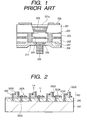
- FIG. 1 A basic structure of a prior art VCSEL is shown in Fig. 1 . It has a structure wherein laser light is vertically emitted through a substrate 201 and 99% or more highly reflective films 209 are provided on both sides of an epitaxially grown layer of several ⁇ m thick.
- reference numeral 202 denotes an etching stop layer; 203 and 205, clad layers; 204, an active layer; 206, a contact layer; 207, an insulating layer; 208, electrodes; and 210, a buried layer.
- the reflective films multiple layers formed of ⁇ /4-thick films having different refractive indexes are chiefly used.
- dielectrics as in the example shown in Fig. 1 or epitaxially grown semiconductors are commonly used.
- epitaxially grown mirrors include those in which an AlAs/GaAs multi-layer film mirror, an active layer and so forth are formed on a GaAs substrate by one-time growth as disclosed in ELECTRONICS LETTERS, 31, p.560 (1995 ), and those in which a GaAs/AlAs mirror formed on a GaAs substrate is bonded by direct joining to a laser structure of an InGaAsP/InP system grown on an InP substrate as disclosed in APPLIED PHYSICS LETTER, 66, p.1030 (1995 ).
- the refractive indexes can not be made so much different that many layers must be formed, which take a long growth time and give a large layer thickness, and hence a low productivity may result and the films can be worked or smoothed with difficulty.
- a practical material is GaAs/AlAs under the existing conditions, which, however, taking account of lattice constant, may impose limitations on materials usable for the active layer, resulting in limitations on oscillation wave bands.
- materials usable for the active layer can be selected from a broader range and the films can also be applied to other wave bands.
- the dielectric multi-layer film mirror can be produced simply, but can not be formed on the substrate as it is.
- the films must be formed after the back of the substrate 201 is etched to make a window 201a as shown in Fig. 1 , where the window is required to be formed with precision and also windows can not be made so much close to each other.
- the yield and uniformity are so poor that the device can not be formed in a high density, and hence there has been a problem when formed in two-dimensional array.
- Japanese Patent Application Laid-open No. 9-223848 discloses a method comprising epitaxially growing on a semiconductor substrate, semiconductor layers having a semiconductor active layer, bonding this semiconductor substrate to an integrated-circuit substrate, and thereafter removing the semiconductor substrate to fabricate a semiconductor device on which a surface-emitting semiconductor device and other electrical devices are integrated.
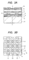
- a schematic cross-sectional view of this semiconductor device is shown in Fig. 2 .
- Fig. 2 A schematic cross-sectional view of this semiconductor device is shown in Fig. 2 .
- reference numeral 500 denotes a light input-output substrate
- 500A light-receiving elements
- 500B vertical oscillator type surface-emitting lasers
- 500C and 500D are each wiring for the light-receiving elements 500A and surface-emitting lasers 500B
- 200 an integrated-circuit substrate
- 200A metal wiring of the integrated-circuit substrate 200
- 300 an insulating layer
- 400 wiring
- L o output light
- L i an input light.
- the semiconductor device shown in Fig. 2 is not a device making use of a substrate comprised of a light-transmitting material so that the light is emitted from the substrate side. Also, the semiconductor device shown in Fig. 2 is provided with wiring at terraced portions at each light-emitting area, and hence has had a problem that it is difficult to form the wiring to bring about a poor yield. Especially when the dielectric multi-layer film mirror is fabricated on the semiconductor layer under the constitution shown in Fig. 2 , a remarkably low yield may result.
- the substrate was removed by a new substrate removal process and the lasers were bonded to an aluminised silicon substrate using a Pd/Ge/InSn contact. Threshold currents below 5.5 mA and output powers of ca. 1 mW were obtained for 40 ⁇ m VCSELs bonded to Si.
- An object of the present invention is to solve the problems in the above prior art to provide a method by which a surface-emitting semiconductor device can be fabricated simply and at a high yield.
- a VCSEL array of a first embodiment according to the present invention is constituted of an InP substrate which is a semiconductor single-crystal substrate, and a wavelength 1.3 ⁇ m band VCSEL of an InGaAs/InGaAsP system grown on the substrate; the VCSEL being bonded to a silica glass substrate.
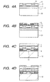
- a cross-sectional structure of the VCSEL array at its one light-emitting region (a pixel) is shown in Fig. 3A .
- the present embodiment has a structure wherein a semiconductor active layer 3 is sandwiched between clad layers 2 and 4 comprised of n-type and p-type semiconductors, respectively, and dielectric multi-layer film mirrors 9 and 10 are formed on the both sides.
- the dielectric multi-layer film mirror 9 is bonded to a glass substrate 12 with an adhesive 11.
- the array structure as viewed on the side opposite to the glass substrate 12 has a plan view as shown in Fig. 3B .
- Electrodes 7 on the side of the glass substrate 12 are previously formed by patterning in stripes, and are led out by removing a semiconductor substrate bonded to the glass substrate 12 and on which an epitaxially grown layer 15 has been formed, and thereafter partly removing the epitaxially grown layer 15 to uncover the electrodes 7.
- Electrodes 8 on the side opposite to the glass substrate 12 are led out by partly removing the dielectric multi-layer film mirror 10.
- Fig. 3B for example, only the left uppermost pixel among pixels 14 is oscillated upon application of a voltage between C1 and L1 through electrode wires 16 (C1-C3 and L1-L3).
- an n-InGaAs contact and etching stop layer 1 an n-InP clad layer 2, an undoped InGaAs/InGaAsP, distorted multi-quantum-well active layer 3, a p-InP clad layer 4 and a p-InGaAs contact layer 5 are grown in this order on an n-InP substrate 20 (the first substrate) by Chemical Beam Epitaxy (CBE).
- CBE Chemical Beam Epitaxy
- the periphery of a light-emitting region is vertically etched in a doughnut of 20 ⁇ m in internal diameter and 40 ⁇ m in external diameter, down to the lower part of the active layer 3 by Reactive Ion Beam Etching (RIBE).
- RIBE Reactive Ion Beam Etching
- the side wall of the InGaAs contact layer 5 is covered with a resist and only the side wall of the active layer 3 is etched by several ⁇ m by selective wet etching to make the active layer constricted in a circle of about 15 ⁇ m diameter.
- a gain anisotropy occurs in the active layer 3 and hence the polarization of oscillated light is stabilized, so that noises such as kinks can be removed which are ascribable to unstable polarization of oscillated light and have been questioned in conventional VCSELs.
- the grooves produced by the selective wet etching are filled up with polyimide 13 or the like.
- an SiN film 6 is formed in order to ensure the insulation at the periphery of one pixel, and Cr(500 ⁇ )/Au (5,000 ⁇ ) (1nm ⁇ 10 ⁇ ) is vapor-deposited deposited as a p-side electrode 7.
- the electrode 7 and contact layer 5 are removed in the form of a circle with a diameter a little larger than that of the active layer 3, and a dielectric multi-layer film 9 consisting of 6 pairs of Si/Al 2 O 3 each layer of which has a thickness of ⁇ /4 ( ⁇ is in-film actual wavelength of oscillation wavelength) is formed by RF sputtering.
- annealing is previously made for ensuring electrode contact.
- the InP substrate 20 is abraded to a thickness of 100 ⁇ m, and the dielectric multi-layer film 9 side is bonded with an adhesive 11 to a glass substrate 12 (the second substrate) comprised of silica glass or the like.
- the adhesive 11 an adhesive may be used which is transparent to visible light and is of the type that softens upon heating.
- the periphery of the substrate 20 is protected and is etched away with hydrochloric acid to uncover the n-InGaAs contact and etching stop layer 1. Since the InGaAs is not etched with hydrochloric acid, the etching completely stops at the contact layer 1.
- the InP substrate 20 may be removed by abrasion or wet etching.
- n-side electrode 8 AuGe(2,000 ⁇ )/Au(3,000 ⁇ ) is vapor-deposited as an n-side electrode 8.
- the electrode 8 and the contact layer 1 are removed in the form of a circle with a diameter a little larger than that of the active layer 3, followed by annealing for ensuring the electrode contact.
- a dielectric multi-layer film 10 consisting of 6 pairs of Si/Al 2 O 3 is formed by RF sputtering.
- the light-emitting regions (pixels) can be arranged in two-dimensional array on the original semiconductor substrate 20, and hence a surface-emitting type array device can be made up with ease.
- the semiconductor substrate 20 which is a substrate on which the layers are grown is not provided with holes conventionally made, but made flat by etching in its entirety, there can be no limitations on the distance between elements (pixels) and the yield.
- how to lead out electrodes must be elaborated. This is because electric currents must be fed in from the lateral side of the dielectric multi-layer film mirror 9 and the electric currents must be taken out from the lateral side of the dielectric multi-layer film mirror 10.
- the device can be made large-area. Namely, although the device is usually limited by the size of the semiconductor substrate (about 3 inches in the case of compound semiconductors), epitaxially grown layers formed on semiconductor substrates may be bonded to the glass substrate, whereby the device can be made more large-area than that.
- latticed grooves may preferably be cut previously by RIBE between the pixels 14 in order to prevent such interference of electric currents. This may be done before the electrodes are attached. In that instance, the grooves may be filled up with polyimide or the like, thus the stripe pattern as shown in Fig. 3B can be formed without cut of the electrodes.
- the temperature control may be made by bringing the dielectric multi-layer film 10 side into adhesion to a heat sink made from diamond, AlN or Si. Since the mirror 10 constituted of Si/Al 2 O 3 has a relatively high thermal conduction, it becomes possible to effect the stable and continuous oscillation. In this instance, light may be emitted from the glass substrate 12 side, the side opposite to the heat sink. Also, non-reflective coating may be applied on the glass substrate 12 so that the light output can be made larger.
- Such an array laser can be applied as a two-dimensional array light source for light information processing, high speed parallel information transmission or light interconnection.
- the array device as described above may be formed using materials capable of emitting blue or ultraviolet light and phosphors of R, G and B may be coated on the glass surface so that it can be applied as a full-color display device.
- the device is fabricated using the InGaAsP/InP system on the InP substrate 20.
- the device may be applied to an AlGaN/InGaN system on a sapphire substrate and an InGaAlP/InAlP, InGaAs/AlGaAs or InGaNAs/AlGaAs(GaInP) system on a GaAs substrate.
- a 1.3 ⁇ m band laser constituted of the InGaNAs/AlGaAs(GaInP) system has so superior temperature characteristics and differential gain that it can be operated without temperature control and, since no heat sink is used, light can be emitted from the top-and-bottom both sides.
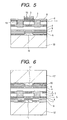
- Fig. 5 is a schematic cross-sectional view showing a second embodiment of the surface-emitting semiconductor device of the present invention.
- the same members as those in Fig. 3A are denoted by same reference numerals, and detailed description thereon is omitted.
- pixels are formed after the first substrate has been bonded to the second substrate.
- a wavelength 1.55 ⁇ m band VCSEL of the InGaAsP/InP system on an InP substrate (the first substrate) is made up.
- a double-side polished silicon substrate is used, which may little cause loss at the wavelength of 1.55 ⁇ m.
- the final layer of the dielectric mirror is previously formed as an amorphous Si layer by sputtering, where the Si layer side is directly bonded to the surface of the silicon substrate to directly joining them while heating at 200°C under application of a load. Accordingly, no adhesive is used.
- the pixels are fabricated in advance, it is difficult to join them to the silicon substrate because of influences of surface irregularities and polyimide. In order to attain a joint strength, the surfaces may be further treated at a high temperature.
- the laser structure is formed by epitaxial growth in the same manner as in the first embodiment (the active layer 3 is designed differently), and Ti(500 ⁇ )/Pt(1,000 ⁇ )/Au(3,000 ⁇ ) is formed as a non-alloy electrode 7 on an InGaAs contact layer 5, the uppermost layer. In this electrode 7, no diffusion takes place at the time of heating.
- the electrode 7 and contact layer 5 are removed in the form of a circle with such a diameter that the effective diameter of the multi-layer film mirror 9 can be a little larger than the diameter of the active layer 3, and then the Si/Al 2 O 3 multi-layer film mirror 9 is formed (the final layer is an Si layer).
- the Si layer side of the multi-layer film mirror 9 is joined to the silicon substrate 18.
- Reference numeral 19 denotes an air gap.
- the method to form pixels is carried out in the same manner as in the first embodiment (e.g., the formation of doughnut-like grooves, the selective etching to constrict the diameter of the active layer 3, and the filling of the grooves with polyimide).
- the electrode 8 is vapor-deposited over the whole surface for the purpose of simplifying the method, but may be formed in the manner as in the first embodiment. In such an instance, light can be emitted also from this side.
- the temperature When the device is operated, the temperature may be controlled in the manner as in the first embodiment.
- Light may be emitted from the side of the silicon substrate 18, or may be emitted from the side on which the silicon substrate 18 is not bonded as a heat sink.
- the integrated circuit fabricated on the semiconductor material silicon substrate and the optical device can be provided on the same substrate 18.
- an optical-electronic integrated device can be made up at a low cost.
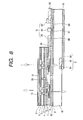
- FIG. 8 An example of a semiconductor device comprising an electronic circuit integrated in this way is shown in Fig. 8 .
- Fig. 8 the same members as those in Fig. 5 are denoted by same reference numerals, and detailed description thereon is omitted.
- a transistor Tr fabricated on a final-stair silicon-on-insulator (SOI) substrate in order to drive the surface-emitting laser is illustrated, and an LSI (not shown) is formed on other region of the silicon substrate 18.
- a photodetector D is also integrated on the silicon substrate 18 on its side not bonded, where laser-light signals can be received. This is effective when the silicon substrate is transparent to laser light.
- a laser output L may be taken out from the side opposite to the silicon substrate 18 or may be taken out from the part where the photodetector is not provided.
- the surface-emitting laser shown in this drawing is a little different from the one shown in Fig. 5 , in which the electrode 8 is formed beneath the dielectric mirror 10 and also windows are made so that the light can be emitted therethrough.
- electrodes are separated by a separating region 95.
- the transistor Tr is an npn-type transistor wherein an electrode 83 of an n + -type diffused region 86 serves as a collector; an electrode 85 of a p-type diffused region 88, a base; and an electrode 84 of an n-type diffused region 87, an emitter.
- Reference numeral 82 denotes an n-type Si thin film on the SOI substrate; 81, an SiO 2 film of the SOI substrate; and 94, a p-type diffused region for the purpose of device separation.
- the collector electrode 83 of the transistor is connected with wiring 7 of the surface-emitting laser.
- Electrodes (not shown) other than the collector of this transistor are connected through other CMOS circuits formed on this Si device and through electric wiring formed on an insulating film 92.
- the other electrode 8 of the surface-emitting laser is also connected to a power source via a wiring pattern formed on the substrate.
- the photodetector D it has a p-type diffused region 90 and an n-type diffused region 91 which are formed on the back of the SOI substrate, and is connected with other CMOS circuit through wiring 89 via an insulating film 93.
- Fig. 6 is a schematic cross-sectional view showing a third embodiment of the surface-emitting semiconductor device of the present invention.
- the same members as those in Fig. 3A are denoted by same reference numerals, and detailed description thereon is omitted.
- the present embodiment is different from the first embodiment in that a third substrate 12' is bonded onto the dielectric multi-layer film mirror 10 via an adhesive 11', and is identical to the first embodiment in other constituents. Accordingly, the surface-emitting semiconductor device of the present embodiment is fabricated in entirely the same manner as the first embodiment before the step of bonding it to the third substrate 12'.
- the device can be a device that emits light from both sides of the active layer.
- a silicon substrate may also be used as the third substrate 12'.
- devices such as transistors may be formed so that a semiconductor device on which the light-emitting device and other electrical devices are integrated can be obtained.
- a semiconductor device can be made up which has a structure wherein integrated circuits fabricated on these silicon substrates are electrically isolated from each other while transmitting signals at a high speed across these integrated circuits.
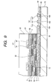
- An example of such a semiconductor device is shown in Fig. 9 .
- the semiconductor device shown in Fig. 9 employs GaAs system semiconductor as a constituent and the oscillating wavelength is 0.83 ⁇ m band.
- the active layer 97 has a multi-quantum-well structure of GaAs/AlGaAs.
- DBR Distributed Bragg's Reflection
- mirrors 96 and 98 comprise an epitaxial multi-layer film of AlAs/AlGaAs.
- a layer having a multi-quantum well structure of InGaAs/GaAs may be used as the active layer 97 to form the semiconductor device of oscillating wavelength of 0.98 ⁇ m band.
- Fig. 9 the same members as those in Fig. 6 are denoted by same reference numerals, and detailed description thereon is omitted.
- LSIs (not shown) are formed on the SOI substrate 18 and silicon substrate 18', and an open drain type MOS-FET 140 at the final-stair n-channel is connected to the surface-emitting laser, where data signals sent from the LSIs are converted into blinking of light.
- the MOS-FET 140 is constituted of a p-type diffused well 103 formed in an n-type diffused layer 99 on the SOI substrate 18.
- an electrode 101 formed via an insulating film 92 serves as a gate; an electrode 100 formed on an n-type diffused layer 104, a drain; and an electrode 102 similarly formed on an n-type diffused layer 105, a source.
- the drain 100 is connected with the surface-emitting laser through electrode wiring 7.
- a photodetector 141 with which optical signals sent from the surface-emitting laser are converted into electric signals is integrated. Its output is taken in as data signals of the LSI on its substrate.
- This photodetector has the same structure as that shown in Fig. 8 .
- the light emitted from an active layer 97 is not transmitted through the SOI substrate 18 and silicon substrate 18'. Then, the active layer 97 is sandwiched on its both sides between Distributed Bragg's Reflection (DBR) mirrors 96 and 98 formed by epitaxial growth, to constitute the surface-emitting semiconductor laser. Thus, a three-dimensionally stacked high-density integrated semiconductor device is obtained.
- DBR Distributed Bragg's Reflection
- the dielectric mirror is formed on a semiconductor layer epitaxially grown.
- the dielectric mirror may previously be formed on the side of a different kind of substrate made of glass or silicon, and may be bonded to the semiconductor layer.
- the mirror can be formed flatly, but gaps are made even in the epitaxially grown layer and the mirror, resulting in a large oscillator length, and also a loss such as scattering may occur to cause an increase in laser threshold electric currents.
- a laser or LED that emits blue to ultraviolet light (420 to 380 nm) by the use of a GaN material is bonded to a glass substrate as in the above embodiment so as to form a two-dimensional array.
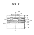
- a phosphor 63 capable of emitting fluorescence of R, G or B may be coated for each pixel so that the device can be applied as a full-color display device that utilizes excitation by light of blue to ultraviolet light.
- the pixels can be accomplished as those of 25 ⁇ m in pixel diameter and 75 ⁇ m in distance, and they can also be made to have a very large area in theory. Hence, a thin-type large-area full-color display device can be provided.
- a low-threshold laser is used as a light-emitting source, and hence display with a small power consumption and a high luminance can be made, bringing about advantages that any high voltage and vacuum are unnecessary.
- a GaN or an AlN low-temperature buffer layer (not shown) formed at a low growth temperature is formed in a thickness a little as large as tens of ⁇ m, and also a clad layer 51 comprised of n-GaN/n-AlGaN, a multi-quantum-well active layer 52 comprised of undoped InGaN/AlGaN, a clad layer 54 comprised of p-AlGaN/p-GaN and a p-GaN cap layer 55 are formed by Metal Organic Vapor Phase Epitaxy (MOVPE).
- MOVPE Metal Organic Vapor Phase Epitaxy
- pixels are formed by etching such as RIBE.
- etching such as RIBE.
- an electric-current blocking region 53 is formed by selective oxidation of the AlGaN layer constituting the active layer 52 and serving as a barrier layer. This utilizes the fact that a heat treatment made in an atmosphere of water vapor at about 500°C causes oxidation to progress inward from side walls with time in the layer containing Al, which is readily oxidizable.
- the side walls of the AlGaN layer of the clad layer 54 are simultaneously oxidized, but the cap layer 55, which is formed of GaN, does not change and no electric-current blocking region is formed. Thus, there may occur no problem.
- grooves are filled up with a fill-up layer 64, and thereafter Ni(1,000 ⁇ )/Au (3,000 ⁇ ) is vapor-deposited as a p-side electrode 57.
- Reference numeral 56 denotes an insulating layer.
- a dielectric multi-layer film mirror 59 comprised of 18 pairs of SiO 2 /MgO is formed by RF sputtering, and is bonded with an adhesive 61 to a glass substrate 62 on which phosphors 63 of R, G and B have been appropriately patterned correspondingly to the pixels.
- the sapphire substrate is removed by abrasion or the like until the buffer layer appears.
- the GaN or AlN low-temperature buffer layer having thus appeared is removed by etching with phosphoric acid heated to 300°C.
- the n-GaN layer of the clad layer 51 formed of single-crystal, epitaxially grown n-GaN/n-AlGaN has so low an etching rate to the etchant that it can be selectively etched.
- a dielectric multi-layer film mirror 60 comprised of SiO 2 /MgO and, as an n-side electrode 58, Ti(500 ⁇ )/Al(1 ⁇ m)/Au(2,000 ⁇ ) are vapor-deposited to complete the device.
- Electrode patterns and electrodes may be provided in the same manner as in the first embodiment.
- the dielectric mirror 59 on the side of the phosphors 63 may be omitted.
- the devices may be made into LED array without providing the mirror on the side from which the light is emitted.
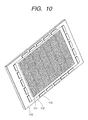
- FIG. 10 An example of a full-color display device fabricated using the surface-emitting semiconductor device of the fourth embodiment shown in Fig. 7 is shown in Fig. 10 .
- GaN light-emitting devices 111 of about 60 mm square unit are arranged in plurality on a glass plate 110 for the display device to make up the device.
- the area depicted round in the light-emitting device corresponds to one pixel.
- Fig. 10 is a perspective view of a full-color flat type display device as viewed on the back.
- Reference numeral 112 denotes a wiring region, and 113 represents how a driver IC for lightening the pixels is mounted on the glass surface.
- the number of the GaN light-emitting devices illustrated in Fig. 10 is not limited to that shown in the drawing.
- the glass plate area may be made larger and a larger number of devices may be integrated so that the device can be adapted to a large-area device of about 60 inches.
- GaN light-emitting layers may be transferred to silicon wafers integrated thereon with drive circuits, by removing GaN light-emitting layers from sapphire substrates, and these may be arranged on a glass plate coated with phosphors to make up the device. More specifically, the device has a structure wherein the GaN light-emitting layers are sandwiched between glass and silicon substrates so that the display light is emitted from the glass side.
- the drive circuits can be integrated on the silicon substrates, and hence the display speed can be improved.
- some sheets of the 60 mm square GaN light-emitting devices 111 may be integrated on a silicon wafer 120 so as to be bonded in plurality to the glass plate after cutting off the peripheral portion having no pixel. Employment of such a step brings about improvements in, e.g., the readiness of alignment of pixels when devices are bonded in plurality, the readiness in processing such as abrasion and the alignment precision of wiring, bringing about an improvement in yield.
- Fig. 11 shows an example in which the devices are bonded to the silicon wafer 120 and the sapphire substrate is removed before they are bonded to the glass substrate, where an arrangement corresponding to RGB is illustrated.
- the pixels are so made up as to stand densest and so arranged that the arrangement of RGB is in the form of a triangle and its vertex and base alternate.
- the manner of arrangement of RGB is not limited to that shown in this drawing, and the proportion of the number of pixels may be controlled in accordance with the luminance of each color.
Landscapes
- Physics & Mathematics (AREA)
- Optics & Photonics (AREA)
- Engineering & Computer Science (AREA)
- Condensed Matter Physics & Semiconductors (AREA)
- General Physics & Mathematics (AREA)
- Electromagnetism (AREA)
- Nanotechnology (AREA)
- Chemical & Material Sciences (AREA)
- Biophysics (AREA)
- Crystallography & Structural Chemistry (AREA)
- Life Sciences & Earth Sciences (AREA)
- Semiconductor Lasers (AREA)
- Led Devices (AREA)
- Devices For Indicating Variable Information By Combining Individual Elements (AREA)
- Led Device Packages (AREA)
Claims (16)
- Verfahren zur Herstellung einer oberflächenemittierenden Halbleitervorrichtung, das die Schritte umfasst:Epitaktisches Wachsen von Halbleiterschichten (51-54) auf einem ersten Substrat (20), das einen Halbleiter, einen Saphir oder ein Glas umfasst, wobei zumindest eine der Halbleiterschichten (51-54) eine aktive Halbleiterschicht (52) hat, die fähig ist, Licht unter Zuführung eines elektrischen Stroms zu emittieren,wobei die Halbleiterschichten (51-54) eine Strom einschränkende Struktur haben, um den Fluss von elektrischem Strom, der zu der aktiven Halbleiterschicht (52) zugeführt wurde, zu begrenzen;gekennzeichnet durchBilden einer Spiegelschicht (59) auf den Halbleiterschichten (51-54), nachdem die eine Strom einschränkende Struktur gebildet wurde;Bonden des ersten Substrats (20) mit einem zweiten Substrat (62), so dass die Halbleiterschichten (51-54) und die Spiegelschicht (59) zwischen den Substraten positioniert sind; undEntfernen des ersten Substrats (20) von den gebondeten Substraten, um die Halbleiterschichten (51-54) und die Spiegelschicht (59) auf dem zweiten Substrat (62) zu belassen,wobei das zweite Substrat (62) einlichtdurchlässiges Material umfasst, welches fähig ist, das Licht durchzulassen.
- Verfahren gemäß Anspruch 1, wobei die eine Strom einschränkende Struktur durch Ätzen eines Teils der aktiven Halbleiterschicht (52) gebildet wird.
- Verfahren gemäß Anspruch 1, das weiterhin einen Schritt des Bildens einer Wärmesenke auf den Halbleiterschichten (51-54) nach dem Entfernen des ersten Substrats (20) umfasst.
- Verfahren gemäß Anspruch 1, das weiterhin einen Schritt des Bildens einer Elektrode (57) auf der Halbleiterschicht umfasst, nachdem die Strom einschränkende Struktur gebildet wurde.
- Verfahren gemäß Anspruch 3, wobei die Spiegelschicht (59) eine oder mehrere dielektrische Mehrschichtenfilme oder einen oder mehrere Mehrschichten-Halbleiter-Filme umfasst.
- Verfahren gemäß Anspruch 1, wobei der Schritt des Entfernens mittels Polieren oder Ätzen des ersten Substrats (20) durchgeführt wird.
- Verfahren gemäß Anspruch 1, wobei das erste Substrat (20) mit dem zweiten Substrat (62) mittels eines dazwischen gestellten Phosphor-Materials (63) gebondet wird.
- Verfahren gemäß Anspruch 7, das weiterhin einen Schritt des Bildens einer nicht reflektierenden Überzug auf einer Seite umfasst, die der Seite gegenüber liegt, mit der das zweite Substrat (62) gebondet wurde.
- Verfahren gemäß Anspruch 1, wobei das zweite Substrat (62) ein Glassubstrat umfasst.
- Verfahren gemäß Anspruch 1, wobei das zweite Substrat (62) ein Halbleitersubstrat umfasst, auf dem ein elektronischer Schaltkreis gebildet wurde.
- Verfahren gemäß Anspruch 1, das weiterhin, nach dem Schritt des Entfernens, einen Schritt des Bildens eines zweiten reflektierenden Spiegels (60) auf der Oberfläche der unbedeckten Halbleiterschichten (51-54) umfasst.
- Verfahren gemäß Anspruch 11, wobei der zweite reflektierende Spiegel (60) mittels einem oder mehreren dielektrischen Mehrschichtfilmen gebildet wird.
- Verfahren gemäß Anspruch 1, wobei die Elektrode (57) eine positive Elektrode und eine negative Elektrode umfasst, welche in einer Matrix angeordnet sind.
- Verfahren gemäß Anspruch 1, wobei eine Vielzahl der ersten Substrate (20), wobei auf jedem davon die Halbleiterschichten (51-54) gebildet wurden, mit dem zweiten Substrat (62) in einem Array gebondet werden, und wobei danach die ersten Substrate (20) von dem zweiten Substrat (62) entfernt werden.
- Verfahren gemäß Anspruch 1, wobei die Halbleiterschichten (51-54) einen Verbindungshalbleiter aus einem der Elemente B, Al, Ga und In mit N umfassen.
- Verfahren gemäß Anspruch 1, wobei die eine oder die mehreren Halbleiterschichten (51-54) eine aktive Halbleiterschicht (52), die ZnO und eine ZnMgO umfassende Mantelschicht umfasst.
Applications Claiming Priority (6)
| Application Number | Priority Date | Filing Date | Title |
|---|---|---|---|
| JP223081/97 | 1997-08-05 | ||
| JP22308197 | 1997-08-05 | ||
| JP22308197 | 1997-08-05 | ||
| JP22938398 | 1998-07-30 | ||
| JP229383/98 | 1998-07-30 | ||
| JP22938398A JPH11154774A (ja) | 1997-08-05 | 1998-07-30 | 面発光半導体デバイスの製造方法、この方法によって製造された面発光半導体デバイス及びこのデバイスを用いた表示装置 |
Publications (3)
| Publication Number | Publication Date |
|---|---|
| EP0896405A2 EP0896405A2 (de) | 1999-02-10 |
| EP0896405A3 EP0896405A3 (de) | 2000-10-04 |
| EP0896405B1 true EP0896405B1 (de) | 2009-10-14 |
Family
ID=26525264
Family Applications (1)
| Application Number | Title | Priority Date | Filing Date |
|---|---|---|---|
| EP98114650A Expired - Lifetime EP0896405B1 (de) | 1997-08-05 | 1998-08-04 | Verfahren zur Herstellung einer oberflächenemittierenden Halbleitervorrichtung |
Country Status (4)
| Country | Link |
|---|---|
| US (1) | US6261859B1 (de) |
| EP (1) | EP0896405B1 (de) |
| JP (1) | JPH11154774A (de) |
| DE (1) | DE69841235D1 (de) |
Cited By (2)
| Publication number | Priority date | Publication date | Assignee | Title |
|---|---|---|---|---|
| US7691659B2 (en) | 2000-04-26 | 2010-04-06 | Osram Gmbh | Radiation-emitting semiconductor element and method for producing the same |
| US7939844B2 (en) | 2000-05-26 | 2011-05-10 | Osram Gmbh | Light-emitting-diode chip comprising a sequence of GAN-based epitaxial layers which emit radiation and a method for producing the same |
Families Citing this family (52)
| Publication number | Priority date | Publication date | Assignee | Title |
|---|---|---|---|---|
| JPH11168263A (ja) | 1997-09-30 | 1999-06-22 | Canon Inc | 光デバイス装置及びその製造方法 |
| US6280523B1 (en) * | 1999-02-05 | 2001-08-28 | Lumileds Lighting, U.S., Llc | Thickness tailoring of wafer bonded AlxGayInzN structures by laser melting |
| US20010042866A1 (en) * | 1999-02-05 | 2001-11-22 | Carrie Carter Coman | Inxalygazn optical emitters fabricated via substrate removal |
| US6320206B1 (en) | 1999-02-05 | 2001-11-20 | Lumileds Lighting, U.S., Llc | Light emitting devices having wafer bonded aluminum gallium indium nitride structures and mirror stacks |
| WO2000058999A2 (en) * | 1999-03-26 | 2000-10-05 | Matsushita Electric Industrial Co., Ltd. | Semiconductor structures having a strain compensated layer and method of fabrication |
| DE60042187D1 (de) | 1999-06-09 | 2009-06-25 | Toshiba Kawasaki Kk | Bond-typ Halbleitersubstrat, lichtemittierendes Halbleiterbauelement und Herstellungsverfahren |
| JP3990846B2 (ja) * | 1999-08-27 | 2007-10-17 | キヤノン株式会社 | 面型光素子、その製造方法、およびこれを用いた装置 |
| US6586781B2 (en) * | 2000-02-04 | 2003-07-01 | Cree Lighting Company | Group III nitride based FETs and HEMTs with reduced trapping and method for producing the same |
| TW497277B (en) * | 2000-03-10 | 2002-08-01 | Toshiba Corp | Semiconductor light emitting device and method for manufacturing the same |
| DE10051465A1 (de) | 2000-10-17 | 2002-05-02 | Osram Opto Semiconductors Gmbh | Verfahren zur Herstellung eines Halbleiterbauelements auf GaN-Basis |
| JP5523277B2 (ja) * | 2000-04-26 | 2014-06-18 | オスラム オプト セミコンダクターズ ゲゼルシャフト ミット ベシュレンクテル ハフツング | 発光半導体素子並びに発光性半導体素子の製造方法 |
| WO2001084640A1 (de) | 2000-04-26 | 2001-11-08 | Osram Opto Semiconductors Gmbh | LUMINESZENZDIODENCHIP AUF DER BASIS VON GaN UND VERFAHREN ZUM HERSTELLEN EINES LUMINESZENZDIODENBAUELEMENTS |
| JP4540201B2 (ja) * | 2000-09-13 | 2010-09-08 | 独立行政法人産業技術総合研究所 | ZnO系酸化物半導体層を有する半導体装置の製法 |
| US6879612B1 (en) * | 2001-01-23 | 2005-04-12 | Optical Communication Products, Inc. | Temperature insensitive VCSEL |
| AU2002345905A1 (en) * | 2001-06-22 | 2003-01-08 | Peregrine Semiconductor Corporation | Integrated photodetector for vcsel feedback control |
| DE10135806A1 (de) * | 2001-07-23 | 2003-02-13 | Zeiss Carl | Spiegel zur Reflexion elektromagnetischer Strahlung und Beleuchtungs- bzw. Abbildungsverfahren unter Einsatz desselben |
| US6746948B2 (en) * | 2001-09-17 | 2004-06-08 | Matsushita Electric Industrial Co., Ltd. | Method for fabricating semiconductor light-emitting device |
| US6455340B1 (en) * | 2001-12-21 | 2002-09-24 | Xerox Corporation | Method of fabricating GaN semiconductor structures using laser-assisted epitaxial liftoff |
| US6967981B2 (en) | 2002-05-30 | 2005-11-22 | Xerox Corporation | Nitride based semiconductor structures with highly reflective mirrors |
| JP4546051B2 (ja) * | 2002-07-17 | 2010-09-15 | パナソニック株式会社 | 半導体装置の製造方法 |
| US20040211972A1 (en) * | 2003-04-22 | 2004-10-28 | Gelcore, Llc | Flip-chip light emitting diode |
| CN1581526A (zh) * | 2003-08-07 | 2005-02-16 | 松下电器产业株式会社 | 半导体装置及其制造方法 |
| US7719017B2 (en) | 2004-01-07 | 2010-05-18 | Hamamatsu Photonics K.K. | Semiconductor light-emitting device and its manufacturing method |
| JP4116587B2 (ja) | 2004-04-13 | 2008-07-09 | 浜松ホトニクス株式会社 | 半導体発光素子及びその製造方法 |
| DE102004038405A1 (de) * | 2004-08-07 | 2006-03-16 | Fraunhofer-Gesellschaft zur Förderung der angewandten Forschung e.V. | Quantenkaskadenlaser mit reduzierter Verlustleistung |
| JP2006269664A (ja) * | 2005-03-23 | 2006-10-05 | Fuji Xerox Co Ltd | 発光デバイス、光通信システム、および発光デバイスの製造方法 |
| TWI246786B (en) * | 2005-05-09 | 2006-01-01 | Chunghwa Picture Tubes Ltd | Substrate-free flip chip light emitting diode and manufacturing method thereof |
| US7625778B2 (en) | 2005-06-08 | 2009-12-01 | Chunghwa Picture Tubes, Ltd. | Method of manufacturing a substrate-free flip chip light emitting diode |
| US20070019699A1 (en) * | 2005-07-22 | 2007-01-25 | Robbins Virginia M | Light emitting device and method of manufacture |
| JP2007080988A (ja) * | 2005-09-13 | 2007-03-29 | Matsushita Electric Ind Co Ltd | 半導体レーザ装置およびレーザ反射膜の製造方法 |
| JP4958273B2 (ja) * | 2007-01-23 | 2012-06-20 | オンセミコンダクター・トレーディング・リミテッド | 発光装置及びその製造方法 |
| EP2232590A4 (de) * | 2007-12-10 | 2013-12-25 | 3M Innovative Properties Co | Halbleiterleuchtanordnung und verfahren zu ihrer herstellung |
| DE102011015726B9 (de) | 2011-03-31 | 2023-07-13 | OSRAM Opto Semiconductors Gesellschaft mit beschränkter Haftung | Halbleiterchip, Display mit einer Mehrzahl von Halbleiterchips und Verfahren zu deren Herstellung |
| JP6060252B2 (ja) * | 2012-04-04 | 2017-01-11 | マサチューセッツ インスティテュート オブ テクノロジー | Cmosと非シリコン素子とのモノリシック一体化に関する方法 |
| CN111496379B (zh) * | 2014-08-19 | 2022-08-26 | 亮锐控股有限公司 | 用于减少在管芯级激光剥离期间所受机械损伤的蓝宝石收集器 |
| EP3062352A1 (de) * | 2015-02-25 | 2016-08-31 | Alcatel Lucent | Optoelektronische vorrichtung |
| EP3295479B1 (de) * | 2015-05-13 | 2018-09-26 | Lumileds Holding B.V. | Saphirkollektor zur verringerung von mechanischer schädigung während einer laserabhebung auf chipebene |
| JP6770637B2 (ja) * | 2016-09-19 | 2020-10-14 | アップル インコーポレイテッドApple Inc. | 製造方法、及び、光電子デバイスのアレイ |
| US10825952B2 (en) | 2017-01-16 | 2020-11-03 | Apple Inc. | Combining light-emitting elements of differing divergence on the same substrate |
| US11381060B2 (en) | 2017-04-04 | 2022-07-05 | Apple Inc. | VCSELs with improved optical and electrical confinement |
| US10818816B2 (en) * | 2017-11-22 | 2020-10-27 | Advanced Semiconductor Engineering, Inc. | Optical device with decreased interference |
| WO2019116721A1 (ja) * | 2017-12-11 | 2019-06-20 | ソニーセミコンダクタソリューションズ株式会社 | 垂直共振器型面発光レーザ素子の製造方法、垂直共振器型面発光レーザ素子、距離センサ及び電子機器 |
| US11322910B2 (en) | 2019-02-21 | 2022-05-03 | Apple Inc. | Indium-phosphide VCSEL with dielectric DBR |
| US11418010B2 (en) | 2019-04-01 | 2022-08-16 | Apple Inc. | VCSEL array with tight pitch and high efficiency |
| US11374381B1 (en) | 2019-06-10 | 2022-06-28 | Apple Inc. | Integrated laser module |
| JP7351132B2 (ja) * | 2019-07-31 | 2023-09-27 | 株式会社リコー | 面発光レーザ、面発光レーザ装置、光源装置及び検出装置 |
| CN113140960B (zh) * | 2021-03-31 | 2022-04-01 | 西安瑞芯光通信息科技有限公司 | 一种基于化合物半导体材料紫外vcsel芯片及制作方法 |
| US12308618B2 (en) * | 2021-04-26 | 2025-05-20 | Lumentum Operations Llc | Matrix addressable vertical cavity surface emitting laser array |
| US12494618B2 (en) | 2022-09-14 | 2025-12-09 | Apple Inc. | Vertical emitters with integrated final-stage transistor switch |
| DE102022127126A1 (de) * | 2022-09-16 | 2024-03-21 | Trumpf Photonic Components Gmbh | Vertikalemittierendes Halbleiterlaserbauteil, Array und Chip mit Vorzugsrichtung |
| CN115881555B (zh) * | 2022-12-23 | 2024-06-14 | 杰创半导体(苏州)有限公司 | 半导体器件的制作方法 |
| KR20240106364A (ko) * | 2022-12-29 | 2024-07-08 | 엘지디스플레이 주식회사 | 표시장치 |
Family Cites Families (22)
| Publication number | Priority date | Publication date | Assignee | Title |
|---|---|---|---|---|
| US4956844A (en) * | 1989-03-17 | 1990-09-11 | Massachusetts Institute Of Technology | Two-dimensional surface-emitting laser array |
| US5034344A (en) * | 1989-07-17 | 1991-07-23 | Bell Communications Research, Inc. | Method of making a surface emitting semiconductor laser |
| US5031187A (en) * | 1990-02-14 | 1991-07-09 | Bell Communications Research, Inc. | Planar array of vertical-cavity, surface-emitting lasers |
| US5034958A (en) * | 1990-04-19 | 1991-07-23 | Bell Communications Research, Inc. | Front-surface emitting diode laser |
| US5029176A (en) * | 1990-05-11 | 1991-07-02 | Bell Communications Research, Inc. | Monolithic multiple-wavelength laser array |
| US5300788A (en) * | 1991-01-18 | 1994-04-05 | Kopin Corporation | Light emitting diode bars and arrays and method of making same |
| US5258990A (en) * | 1991-11-07 | 1993-11-02 | The United States Of America As Represented By The Secretary Of The United States Department Of Energy | Visible light surface emitting semiconductor laser |
| US5283447A (en) * | 1992-01-21 | 1994-02-01 | Bandgap Technology Corporation | Integration of transistors with vertical cavity surface emitting lasers |
| JP3259931B2 (ja) * | 1992-04-17 | 2002-02-25 | シャープ株式会社 | 半導体発光素子および半導体表示装置 |
| JP3194503B2 (ja) | 1992-06-04 | 2001-07-30 | キヤノン株式会社 | 化合物半導体装置及びその製造方法 |
| US5428634A (en) * | 1992-11-05 | 1995-06-27 | The United States Of America As Represented By The United States Department Of Energy | Visible light emitting vertical cavity surface emitting lasers |
| US5376580A (en) * | 1993-03-19 | 1994-12-27 | Hewlett-Packard Company | Wafer bonding of light emitting diode layers |
| JPH0786691A (ja) * | 1993-09-14 | 1995-03-31 | Sony Corp | 発光装置 |
| US5459081A (en) * | 1993-12-21 | 1995-10-17 | Nec Corporation | Process for transferring a device to a substrate by viewing a registration pattern |
| JP3474917B2 (ja) * | 1994-04-08 | 2003-12-08 | 日本オプネクスト株式会社 | 半導体装置の製造方法 |
| JPH07297476A (ja) * | 1994-04-21 | 1995-11-10 | Hitachi Ltd | 半導体レーザ装置 |
| FR2739230B1 (fr) * | 1995-09-22 | 1997-12-19 | Oudar Jean Louis | Composant d'emission laser a cavite verticale a emission par la surface a une longueur d'onde comprise entre 1,3 et 1,5 mu m et procede pour sa realisation |
| JPH09150549A (ja) * | 1995-09-25 | 1997-06-10 | Kyocera Corp | 画像装置及びその製造方法 |
| US5724376A (en) * | 1995-11-30 | 1998-03-03 | Hewlett-Packard Company | Transparent substrate vertical cavity surface emitting lasers fabricated by semiconductor wafer bonding |
| JP3058077B2 (ja) * | 1996-01-16 | 2000-07-04 | 松下電器産業株式会社 | 半導体受発光装置 |
| JP3236774B2 (ja) | 1996-02-16 | 2001-12-10 | 日本電信電話株式会社 | 半導体集積回路 |
| US5877038A (en) * | 1996-11-27 | 1999-03-02 | The Regents Of The University Of California | Method of making a vertical cavity laser |
-
1998
- 1998-07-30 JP JP22938398A patent/JPH11154774A/ja active Pending
- 1998-08-04 EP EP98114650A patent/EP0896405B1/de not_active Expired - Lifetime
- 1998-08-04 DE DE69841235T patent/DE69841235D1/de not_active Expired - Lifetime
- 1998-08-05 US US09/129,082 patent/US6261859B1/en not_active Expired - Lifetime
Cited By (3)
| Publication number | Priority date | Publication date | Assignee | Title |
|---|---|---|---|---|
| US7691659B2 (en) | 2000-04-26 | 2010-04-06 | Osram Gmbh | Radiation-emitting semiconductor element and method for producing the same |
| US7939844B2 (en) | 2000-05-26 | 2011-05-10 | Osram Gmbh | Light-emitting-diode chip comprising a sequence of GAN-based epitaxial layers which emit radiation and a method for producing the same |
| US8436393B2 (en) | 2000-05-26 | 2013-05-07 | Osram Gmbh | Light-emitting-diode chip comprising a sequence of GaN-based epitaxial layers which emit radiation and a method for producing the same |
Also Published As
| Publication number | Publication date |
|---|---|
| US6261859B1 (en) | 2001-07-17 |
| JPH11154774A (ja) | 1999-06-08 |
| DE69841235D1 (de) | 2009-11-26 |
| EP0896405A3 (de) | 2000-10-04 |
| EP0896405A2 (de) | 1999-02-10 |
Similar Documents
| Publication | Publication Date | Title |
|---|---|---|
| US6261859B1 (en) | Method for fabricating surface-emitting semiconductor device, surface-emitting semiconductor device fabricated by the method, and display device using the device | |
| EP0905838B1 (de) | Oberflächenartige optische Vorrichtung und Herstellungsverfahren | |
| US6658041B2 (en) | Wafer bonded vertical cavity surface emitting laser systems | |
| CN113396486B (zh) | 具有电介质dbr的磷化铟vcsel | |
| US12463404B2 (en) | Vertical cavity surface emitting laser element, vertical cavity surface emitting laser element array, vertical cavity surface emitting laser module, and method of producing vertical cavity surface emitting laser element | |
| US6277696B1 (en) | Surface emitting laser using two wafer bonded mirrors | |
| US5724376A (en) | Transparent substrate vertical cavity surface emitting lasers fabricated by semiconductor wafer bonding | |
| US5732103A (en) | Long wavelength VCSEL | |
| US20050226299A1 (en) | Vertical-cavity surface emitting laser diode | |
| JP2002353568A (ja) | 半導体レーザとそれを用いた光モジュール及び光通信システム | |
| US6835959B2 (en) | Semiconductor device, and method for manufacturing the same | |
| JP7598492B2 (ja) | 面発光半導体レーザおよび面発光半導体レーザを製造する方法 | |
| CN114830467A (zh) | 发光器件和制造发光器件的方法 | |
| US10554018B2 (en) | Hybrid vertical current injection electro-optical device with refractive-index-matched current blocking layer | |
| JPH05283796A (ja) | 面発光型半導体レーザ | |
| JP3093547B2 (ja) | 光集積回路およびその製造方法 | |
| US6859476B2 (en) | Surface-emitting semiconductor laser and method of manufacturing the same | |
| US5346854A (en) | Method of making a semiconductor laser | |
| JP3238979B2 (ja) | 面発光レーザ装置及びその製造方法 | |
| JPH0951142A (ja) | 半導体発光素子 | |
| JP2002100799A (ja) | 半導体受光素子、半導体発光受光装置、およびその作製方法 | |
| JP3469051B2 (ja) | 面発光半導体レーザ | |
| US20240146032A1 (en) | Quantum cascade element | |
| JPH11112096A (ja) | 半導体レーザ装置およびこれを用いた光通信システム | |
| JP2005166870A (ja) | 光素子及びその製造方法、光モジュール、光伝送装置 |
Legal Events
| Date | Code | Title | Description |
|---|---|---|---|
| PUAI | Public reference made under article 153(3) epc to a published international application that has entered the european phase |
Free format text: ORIGINAL CODE: 0009012 |
|
| AK | Designated contracting states |
Kind code of ref document: A2 Designated state(s): DE FR GB IT NL SE |
|
| AX | Request for extension of the european patent |
Free format text: AL;LT;LV;MK;RO;SI |
|
| PUAL | Search report despatched |
Free format text: ORIGINAL CODE: 0009013 |
|
| AK | Designated contracting states |
Kind code of ref document: A3 Designated state(s): AT BE CH CY DE DK ES FI FR GB GR IE IT LI LU MC NL PT SE |
|
| AX | Request for extension of the european patent |
Free format text: AL;LT;LV;MK;RO;SI |
|
| 17P | Request for examination filed |
Effective date: 20010214 |
|
| AKX | Designation fees paid |
Free format text: DE FR GB IT NL SE |
|
| RTI1 | Title (correction) |
Free format text: METHOD FOR FABRICATING SURFACE-EMITTING SEMICONDUCTOR DEVICE |
|
| RIC1 | Information provided on ipc code assigned before grant |
Ipc: H01L 33/00 20060101AFI20090109BHEP |
|
| GRAP | Despatch of communication of intention to grant a patent |
Free format text: ORIGINAL CODE: EPIDOSNIGR1 |
|
| RIC1 | Information provided on ipc code assigned before grant |
Ipc: H01S 5/183 20060101ALI20090326BHEP Ipc: H01L 33/00 20060101AFI20090326BHEP |
|
| GRAS | Grant fee paid |
Free format text: ORIGINAL CODE: EPIDOSNIGR3 |
|
| GRAA | (expected) grant |
Free format text: ORIGINAL CODE: 0009210 |
|
| AK | Designated contracting states |
Kind code of ref document: B1 Designated state(s): DE FR GB IT NL SE |
|
| REG | Reference to a national code |
Ref country code: GB Ref legal event code: FG4D |
|
| REF | Corresponds to: |
Ref document number: 69841235 Country of ref document: DE Date of ref document: 20091126 Kind code of ref document: P |
|
| NLV1 | Nl: lapsed or annulled due to failure to fulfill the requirements of art. 29p and 29m of the patents act | ||
| PG25 | Lapsed in a contracting state [announced via postgrant information from national office to epo] |
Ref country code: SE Free format text: LAPSE BECAUSE OF FAILURE TO SUBMIT A TRANSLATION OF THE DESCRIPTION OR TO PAY THE FEE WITHIN THE PRESCRIBED TIME-LIMIT Effective date: 20091014 |
|
| PLBE | No opposition filed within time limit |
Free format text: ORIGINAL CODE: 0009261 |
|
| STAA | Information on the status of an ep patent application or granted ep patent |
Free format text: STATUS: NO OPPOSITION FILED WITHIN TIME LIMIT |
|
| 26N | No opposition filed |
Effective date: 20100715 |
|
| PG25 | Lapsed in a contracting state [announced via postgrant information from national office to epo] |
Ref country code: IT Free format text: LAPSE BECAUSE OF FAILURE TO SUBMIT A TRANSLATION OF THE DESCRIPTION OR TO PAY THE FEE WITHIN THE PRESCRIBED TIME-LIMIT Effective date: 20091014 |
|
| REG | Reference to a national code |
Ref country code: FR Ref legal event code: ST Effective date: 20110502 |
|
| PG25 | Lapsed in a contracting state [announced via postgrant information from national office to epo] |
Ref country code: FR Free format text: LAPSE BECAUSE OF NON-PAYMENT OF DUE FEES Effective date: 20100831 |
|
| PG25 | Lapsed in a contracting state [announced via postgrant information from national office to epo] |
Ref country code: NL Free format text: LAPSE BECAUSE OF FAILURE TO SUBMIT A TRANSLATION OF THE DESCRIPTION OR TO PAY THE FEE WITHIN THE PRESCRIBED TIME-LIMIT Effective date: 20091014 |
|
| PGFP | Annual fee paid to national office [announced via postgrant information from national office to epo] |
Ref country code: GB Payment date: 20170830 Year of fee payment: 20 |
|
| PGFP | Annual fee paid to national office [announced via postgrant information from national office to epo] |
Ref country code: DE Payment date: 20171030 Year of fee payment: 20 |
|
| REG | Reference to a national code |
Ref country code: DE Ref legal event code: R071 Ref document number: 69841235 Country of ref document: DE |
|
| REG | Reference to a national code |
Ref country code: GB Ref legal event code: PE20 Expiry date: 20180803 |
|
| PG25 | Lapsed in a contracting state [announced via postgrant information from national office to epo] |
Ref country code: GB Free format text: LAPSE BECAUSE OF EXPIRATION OF PROTECTION Effective date: 20180803 |