EP0896665B1 - Systeme de prise de vues pour l'evaluation d'elements d'essais analytiques - Google Patents
Systeme de prise de vues pour l'evaluation d'elements d'essais analytiques Download PDFInfo
- Publication number
- EP0896665B1 EP0896665B1 EP97918153A EP97918153A EP0896665B1 EP 0896665 B1 EP0896665 B1 EP 0896665B1 EP 97918153 A EP97918153 A EP 97918153A EP 97918153 A EP97918153 A EP 97918153A EP 0896665 B1 EP0896665 B1 EP 0896665B1
- Authority
- EP
- European Patent Office
- Prior art keywords
- image recording
- ccd chip
- lens system
- recording system
- image
- Prior art date
- Legal status (The legal status is an assumption and is not a legal conclusion. Google has not performed a legal analysis and makes no representation as to the accuracy of the status listed.)
- Expired - Lifetime
Links
Images

Classifications
-
- G—PHYSICS
- G01—MEASURING; TESTING
- G01N—INVESTIGATING OR ANALYSING MATERIALS BY DETERMINING THEIR CHEMICAL OR PHYSICAL PROPERTIES
- G01N27/00—Investigating or analysing materials by the use of electric, electrochemical, or magnetic means
- G01N27/26—Investigating or analysing materials by the use of electric, electrochemical, or magnetic means by investigating electrochemical variables; by using electrolysis or electrophoresis
- G01N27/416—Systems
- G01N27/447—Systems using electrophoresis
- G01N27/44704—Details; Accessories
- G01N27/44717—Arrangements for investigating the separated zones, e.g. localising zones
- G01N27/44721—Arrangements for investigating the separated zones, e.g. localising zones by optical means
Definitions
- the present invention relates to an image recording system for image recording and evaluation analytical test elements including a recording unit for test elements Lens system, which images a test element in the recording unit on a CCD chip, a CCD chip that takes an image of the test element and to an evaluation unit passes on as well as an evaluation unit, which the signals of the CCD chip in a representation converts an image of the test element, the focus of the lens system being fixed and the lens system is a reduction lens with an aperture on the image side of is at least 0.7, the distance between the CCD chip and the next lens of the lens system is less than 15 mm and this distance is kept constant at least 10 ⁇ m.
- the present invention particularly falls in the field of molecular biology in which Biomolecules with a label or stain are detected as well as their location is determined on a mostly flat analysis medium.
- Biomolecules in the sense of the invention are in particular nucleic acids, nucleic acid fragments and proteins.
- the detection proteins are then mostly available higher detection sensitivity with enzymes such as alkaline phosphatase or Horseradish peroxidase, coupled, which has a color or chemiluminescence reaction on suitable substrates catalyze. Ultimately, these reactions serve as evidence.
- Radioactive methods are still used in the field of labeling nucleic acids much more used than non-radioactive methods, even though they are those with radioactive Disadvantages associated with isotopes.
- the main disadvantages are the short ones Half-life of the isotopes and the hazards posed by radioactive isotopes of health and the environment. For this reason, alternative methods without radioactive Isotopes developed for labeling biomolecules.
- One way is Coupling biomolecules directly with fluorescent dyes, which are then carried out by fluorescence microscopy can be demonstrated.
- Blotting methods Southern, Northern and dot blots for nucleic acids and Western blots for proteins are common.
- fluorescent dyes are for these Areas of application not sensitive enough because of problems with the signal background and Self-fluorescence of the blotting membranes used occur.
- detection on such membranes is by direct or indirect binding of the Proteins on enzymes, such as alkaline phosphatase or peroxidase, possible.
- enzymes catalyze the emission of chemiluminescent light with the addition of suitable substrates.
- nucleic acids with haptens such as. B. digoxigenin or biotin and these labels with specific antibodies, which in turn bind to enzymes are bound to be proven.
- an image of the membrane can be created visually evaluated or photographed with standard devices.
- a chemiluminescent reaction becomes for the detection processes described above used because it is very fast and very sensitive. It has been found that proof is at least as sensitive as radioactive evidence via the chemiluminescence reaction, but can be carried out much faster.
- the object of the present invention was to provide a system for evaluating analytical test elements to provide a high sensitivity with sufficient dynamic range provides and also enables the evaluation of different test elements without a Focus is necessary.
- the above-mentioned object was achieved by an image recording system for evaluation analytical test elements according to claim 1.
- the task can be solved if a special lens system is selected, the image side has a high aperture and a short distance from the sensor. Associated with it is, however, a very shallow depth of field on the image side.
- a lens system according to the invention has a high depth of field on the object side, thereby avoiding focusing can be, if there is a recording unit for the test elements, the distance of test element and lens system essentially determines. Because of the big object-side depth of field of the lens system used, fluctuations in the distance fall between lens system and test element due to fluctuations in the thickness of the test element not weight.
- the image recording system according to the invention is used for image recording and evaluation analytical test elements.
- test elements are, for example, membranes on which Blotting reactions are carried out or gels, such as those used for DNA sequencing be used.
- test elements are also according to the invention suitable on which there are fluorescent or colored analytes. That in the imaging system lens system used is designed so that the advantages in particular for test elements with a size above approx. 4 x 4 cm.
- the receiving unit for flat test elements can, for example, be a plate on which the test elements are put on. However, the receiving unit preferably has the Shape of a drawer, on the bottom surface of which the test elements are placed and with which Drawer can be inserted into the image recording system.
- a recording unit can for example, also consist of guide grooves into which the test element, if necessary a carrier is inserted. According to the invention, the recording unit fulfills the function the test elements at a substantially constant distance from the lens system to be arranged in such a way that the test surface of the test element is perpendicular to the Optical axis of the lens system is arranged and the test element positioned laterally is that the area to be evaluated is detected.
- the distance between the optics and the CCD chip is chosen to be very small and the aperture of the lens system on the side facing the CCD chip is enlarged compared to conventional systems.
- the distance between the last lens surface of the lens system and the CCD chip is less than 15 mm, preferably less than 12 mm.
- the radius of the aperture of the lens system on the side facing the CCD chip is greater than 25 mm, preferably greater than 30 mm.
- the lens system is designed as a reduction optics 1: n with n greater than 10, preferably greater than 14.
- the lens system typically has a focal length of 850 mm on the object side and an aperture ratio of 0.95. The aperture ratio is given by the quotient of the focal length of the optics and the diameter of the entrance pupil.
- the image-side aperture of the lens system is at least 0.7, preferably at least 1.0. Under the aperture on the image side, the angle of the entire entrance pupil is defined in RAD seen at the image level, understood.
- the CCD chip In order to keep distortion as low as possible with a lens as described above and to achieve a high light intensity, the CCD chip must be as close as possible to the lens system be brought up.
- the very low associated with such an arrangement Focal length poses the problem that the distance between the CCD chip and the The main axis of the lens system must be set extremely precisely and kept constant.
- the distance used according to the invention smaller than 15 mm or preferably less than 12 mm, the distance must be kept constant at least 10 ⁇ m, better still 7 ⁇ m to prevent defocusing. This requirement makes you special structure of the holder of the image recording system and CCD chip necessary. in the In connection with the compensator, options are described below, to realize such a constant distance.
- CCD chips with more than 1000 x 1000 pixels and pixel sizes of preferably more than 15 x 15 ⁇ m used. Suitable CCD chips are commercially available and are therefore not described further here.
- the images of the test elements recorded by the CCD chip are sent to an evaluation unit forwarded.
- an evaluation unit is usually a microprocessor that works with a signal conversion unit.
- Such units are called "frame grabbers" designated.
- When evaluating the images an attempt is made to give the user a To offer software that is suitable for the respective problem.
- the software of electrophoresis gels can serve to map the bands on the graphically display and quantify the migrated analyte.
- the user of an image recording system will use it be interested in obtaining an image of the test element on which the analytes are visible.
- the evaluation unit generates an image of the test element and outputs it for example on a monitor or a printer.
- the distance between the lens system and the CCD chip is unusual small and precautions must be taken to keep this distance at least 10 ⁇ m better kept constant at 7 ⁇ m.
- this high distance constancy can be achieved if the brackets for CCD chip and lens system as well as the other materials that define the distance between these units so-called Invar steels can be realized, the extremely low thermal expansion coefficient have.
- Invar steels are expensive and also their processing is complex, other options are preferred according to the invention to maintain the distance to reach.
- a compensator is used the thermally induced changes in distance between the lens system and the CCD chip by a compensates for opposite length changes.
- This can be done, for example, by an arrangement can be achieved in which the CCD chip is mounted on the compensator, which in turn on the bracket of the lens system. The arrangement is chosen so that at a Temperature change the length changes of the housing and that of the compensator are opposed vectorially.
- the compensator is arranged so that a distance change between CCD chip and lens system caused by a thermal Change in length of the compensator is compensated. How the compensator works is explained in more detail in FIG. 3 using an example.
- compensators can be used between the lens system and the CCD chip who make a correction based on a previous measurement of the distance.
- Such compensators can, for example, motor drives, piezo drives or be hydraulics.
- the lens system is not twisted, in order to achieve a focus, as is the case, for example, with photographic Cameras is the case.
- compensators according to the invention take a direct one linear distance change before.
- Piezo elements are particularly suitable.
- the CCD chip is encapsulated in a vacuum. Such an arrangement prevents the ingress of dust or moisture. Furthermore, it has proven to be advantageous to encapsulate a moisture-absorbing material, such as, for example, in the encapsulation. B. silica gel, to remove residual moisture that could deposit on the lenses or the sensor to remove. It is also advantageous to heat the optical window of the encapsulation in order to prevent moisture from depositing on this window. Furthermore, it is advantageous to also encapsulate the space between the above-mentioned window and the lens system (for example N 2 atmosphere) in order to prevent heat dissipation and the ingress of moisture or dust.
- a moisture-absorbing material such as, for example, in the encapsulation.
- B. silica gel to remove residual moisture that could deposit on the lenses or the sensor to remove. It is also advantageous to heat the optical window of the encapsulation in order to prevent moisture from depositing on this window.
- the object-side focus length is for a lens system as described above relatively strongly dependent on the light wavelength used. It has therefore found to be extremely advantageous for measurements at different wavelengths, one Recording unit to choose, the multiple recording positions at different intervals of the lens system.
- a receiving unit can also be used be used depending on the wavelength used for the investigation changes the distance between the test element and the lens system. This can be realized, for example, by a motor-driven table.
- the system has a light-tight housing, that prevents intrusion of ambient light.
- a lighting unit is provided to excite the fluorescent radiation become.
- FIG. 1 shows the representation of an image recording system according to the invention.
- the optics unit (1) is in the upper part of the housing (2).
- the CCD chip (3) which is cooled by an arrangement of Peltier elements (4).
- the heat given off by the Peltier elements (4) is dissipated by a fan.
- the power supply is located in the lower area of the image recording system (7) and the receiving unit (8) for test elements.
- the recording unit shown has the shape of a drawer that can be pulled out of the housing.
- the too Examining test elements are placed on the bottom surface (9) of the drawer and with the drawer inserted into the housing. To ensure that the test elements lie flat To ensure on the floor surface, a glass plate (10) is also provided when pulling out the drawer on one side so that a test element underneath can be pushed. When the drawer is pushed in, the glass plate lowers and presses the test element onto the bottom surface (9) of the drawer.
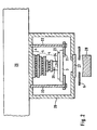
- FIG. 2 shows the area of the CCD chip (3) with temperature control devices within the Encapsulation (20).
- the CCD chip (3) is on a holder (21), which in turn is connected to the encapsulation (20) via spacers (22).
- the CCD chip (3) is attached to the bracket (21) so that it adjusts by rotation about the optical axis and can be fixed in the adjustment position.
- CCD chip fixed on the cooling block (29).
- a corresponding design of the cooling block ensures that the chip is perpendicular to the optical axis.
- the cooling block contains the heating resistor (24) and the temperature sensor (25). Located above the CCD chip (3) a mounting frame (23) with which the CCD chip is pressed onto the cooling block (29) becomes.
- the unit of temperature sensor and The heating resistor is thermally conductive and is connected via a cascade of Peltier elements (4) cooled.
- the top Peltier element gives the heat dissipated to the encapsulation (20) and the encapsulation in turn from a heat sink (26).
- the heat sink will be the same as before mentioned preferably cooled by a fan.
- An optical window (27) can be seen on the underside of the encapsulation. Between the optical window (27) and the first lens (28) of the lens system (5) is located the closure (6).
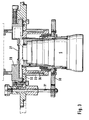
- Figure 3 shows the encapsulation (20) with the window (27) and in particular that the Encapsulation subsequent lens system with holder.
- the lens system is over one "Trumpet construction" consisting of the aluminum cylinder (34) and the steel cylinder (33) connected to the base plate (32).
- the flange plate (32) is on the encapsulation (20) flanged.
- the steel cylinder (33) is fastened to the flange plate (32) (position 35)).
- the aluminum cylinder (34) is attached to the steel cylinder on the side remote from the flange (position 36)) and lies in the flange plane only on the steel cylinder (position 37)).
- the optics (5) is in area near the flange attached to the aluminum cylinder and is at the other end of the aluminum cylinder only guided (see guided tour 39). With thermal changes in length the mounting arrangement (including encapsulation, flange plate, retaining pins, Holding plate etc.) these are compensated for by changing the length of the aluminum cylinder.
- the principle realized in this arrangement is that a change in length the mounting arrangement by changing the length of a compensation element (in this case aluminum cylinder) is compensated.
- the change in length of the compensation element of the change in length of the rest Bracket device is vectorially opposite.
- the thermal expansion coefficient of the compensator is greater than that other materials of the mounting device.
- the described embodiment is based on a compensator that compensates due to its thermal change in length performs. Compensators are somewhat more complex, but also technically feasible, which either measure the length between the CCD chip and the lens system or carry out a temperature measurement and then a distance correction make.
- the system according to the invention is designed so that the user has no focus must be made. However, the manufacturer makes a focus. This focusing takes place via the adjusting wheel (31), which via the gears (30 a) and (30) turns a threaded nut located on the lens system.
- the adjusting wheel (31) which via the gears (30 a) and (30) turns a threaded nut located on the lens system.
- the lens system itself fixed against twisting. Due to manufacturing tolerances the lens system may have slight distortions that are not rotationally symmetrical and would thus also be rotated when the lens system is rotated. Will the lens system secured against rotation, however, any inhomogeneities that may exist determined by test samples and, if necessary, by the evaluation unit be compensated.
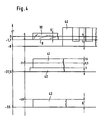
- Figure 4 shows schematically different levels that are realized in a recording unit can.
- the plane marked "0" on the ordinate is 850 mm from the CCD chip away.
- This The plane corresponds to the surface of the base plate (9) already shown in FIG Drawer.
- This level is selected in its distance so that the image recording system for the frequently used luminescence wavelength of 460 nm provides optimal images.
- the system according to the invention cannot only evaluate planar test elements are, but also, for example, microtiter plates (40) as shown schematically in Figure 4.
- a second can be used in the recording unit to evaluate the microtiter plate (40) Plane should be provided, which is at a distance of 8 mm from the zero line. This distance is chosen so that when liquid levels occur in practice in the Caverns of the microtiter plate evaluations can be carried out.
- a third The level is shown at - 27.5 mm. This position is particularly useful for the evaluation of Ethidium bromide gels (41) at 600 nm are suitable. Because the ethidium bromide gels usually be evaluated within a tub (42), the height of the tub when choosing the Level are taken into account.
- a fourth level shown in FIG. 4 is for Fluorescence measurements at 700 nm are well suited.
- a plate is shown schematically in FIG (43) is drawn, which can be charged electrostatically. Can on this plate Membranes are placed so that they are due to the electrostatic interactions adhere. This type of positioning, similar to the glass plate (10), ensures that the The membranes lie flat on the surface and there are no errors due to corrugations.
- the distance to the reference plane or zero plane is on a first ordinate shown.
- the ordinate on the right shows the focal planes used on.
- the focal planes and the contact planes are correct essentially match each other.
- the focal plane at - 21 mm chosen so that it runs through the middle of the gel.
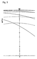
- FIG. 5 shows, using a diagram, the defocusing of the image recording system Change the distance between the plane of the CCD chip and the lens system.
- On the ordinate is the focus in the X direction (solid lines) and the Y direction (dashed lines) for four different spatial frequencies.
- On the Abzissa is represented with 0 the exact focal plane.
- Each tick mark on the abscissa indicates a deviation from the focal plane by 2 ⁇ m. It can therefore be seen from FIG. how exactly the distance between the CCD chip for a lens system according to the invention and lens system must be kept constant in order to obtain sufficient sharpness guarantee.
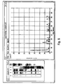
- FIG. 6 is a screen printout of the representation of a DNA chemiluminescence blot shown.
- the left half of the picture is the actual illustration of the DNA chemiluminescence Recognize blots with its bands. To the right of this are the intensities of the bands for the 5. Line of the gel shown. The evaluation can be edited with a menu become.
Landscapes
- Health & Medical Sciences (AREA)
- Life Sciences & Earth Sciences (AREA)
- Molecular Biology (AREA)
- Chemical & Material Sciences (AREA)
- General Physics & Mathematics (AREA)
- Immunology (AREA)
- Physics & Mathematics (AREA)
- Analytical Chemistry (AREA)
- Biochemistry (AREA)
- General Health & Medical Sciences (AREA)
- Chemical Kinetics & Catalysis (AREA)
- Electrochemistry (AREA)
- Pathology (AREA)
- Investigating, Analyzing Materials By Fluorescence Or Luminescence (AREA)
- Investigating Or Analysing Biological Materials (AREA)
- Investigating Or Analysing Materials By The Use Of Chemical Reactions (AREA)
- Investigating Materials By The Use Of Optical Means Adapted For Particular Applications (AREA)
- Testing Of Optical Devices Or Fibers (AREA)
- Solid State Image Pick-Up Elements (AREA)
- Facsimile Heads (AREA)
Claims (22)
- Système de prise de vues pour la prise de vues et l'évaluation d'éléments d'essais analytiques comprenantle foyer du système de lentilles étant fixe, le système de lentilles étant une optique de réduction pourvue d'une ouverture côté image d'au moins 0,7, la distance entre la puce CCD et la lentille suivante du système de lentilles étant inférieure à 15 mm et cette distance étant maintenue constante à au moins 10 µm.une unité de prise de vues pour éléments d'essaisun système de lentilles, qui représente un élément d'essais dans l'unité de prisé de vues sur une puce CCD,une puce CCD, qui prend une image de l'élément d'essais et la transmet à une unité d'évaluation,une unité d'évaluation, qui convertit les signaux de la puce CCD en une représentation d'une image de l'élément d'essais,
- Système de prise de vues selon la revendication 1, dans lequel la distance entre la lentille proche de la puce CCD du système de lentilles et la puce CCD est inférieure à 12 mm.
- Système de prise de vues selon la revendication 1, dans lequel le rayon du diaphragme et du système de lentilles est supérieur à 25 mm, de préférence supérieur à 30 mm.
- Système de prise de vues selon la revendication 1, dans lequel l'ouverture côté image est d'au moins 1,0.
- Système de prise de vues selon la revendication 1, dans lequel la variation de distance due à des effets thermiques entre le système de lentilles et la puce CCD est compensée au moins en partie par un compensateur.
- Système de prise de vues selon la revendication 5, dans lequel le système de lentilles ou la puce CCD est logé sur le compensateur, lui-même logé sur la fixation du système de lentilles ou la puce CCD.
- Système de prise de vues selon la revendication 5, dans lequel le compensateur engendre un mouvement du système de lentilles ou de la puce CCD en raison de son coefficient de dilatation thermique, qui est vectoriellement opposé à la variation de longueur thermique du support du système de lentilles et de la puce CCD.
- Système de prise de vues selon la revendication 6, dans lequel le compensateur est en métal d'aluminium.
- Système de prise de vues selon la revendication 5, dans lequel le compensateur modifie la distance entre le système de lentilles et la puce CCD, afin d'obtenir une image nette.
- Système de prise de vues selon la revendication 9, dans lequel le compensateur est une motorisation, un entraínement piézo-électrique ou un système hydraulique.
- Système de prise de vues selon la revendication 1, dans lequel la puce CCD est encapsulée.
- Système de prise de vues selon la revendication 11, dans lequel un matériau absorbant l'humidité se trouve dans l'encapsulage.
- Système de prise de vues selon la revendication 11, équipé d'une fenêtre chauffable.
- Système de prise de vues selon la revendication 1, équipé d'un dispositif d'ajustage du foyer sans torsion du système de lentilles autour de l'axe optique.
- Système de prise de vues selon la revendication 1, dans lequel l'unité de prise de vues possède deux positions de prise de vues ou plus à différentes distances du système de lentilles.
- Système de prise de vues selon la revendication 1, dans lequel l'unité de prise de vues comporte un dispositif de déplacement avec lequel la distance entre l'élément d'essais et le système de lentilles est modifié.
- Système de prise de vues selon la revendication 1, dans lequel les éléments d'essais sont des gels, des membranes ou des plaques de microtitrage.
- Système de prise de vues selon la revendication 1, équipé d'une unité d'éclairage de l'élément d'essais analytique.
- Système de prise de vues selon la revendication 1, dans lequel l'élément d'essais, le système de lentilles et la puce CCD se trouvent dans un boítier étanche à la lumière.
- Utilisation d'un système de prise de vues pour la prise de vues et l'évaluation selon la revendication 1, pour la prise de vues et l'évaluation de membranes sur la base de signaux chimiluminescents.
- Utilisation d'un système de prise de vues pour la prise de vues et l'évaluation selon la revendication 1, pour la prise de vues et l'évaluation de membranes sur la base de signaux fluorescents.
- Utilisation d'un système de prise de vues pour la prise de vues et l'évaluation selon la revendication 1, pour la prise de vues et l'évaluation de plaques de microtitrage sur la base de signaux chimiluminescents.
Applications Claiming Priority (3)
| Application Number | Priority Date | Filing Date | Title |
|---|---|---|---|
| DE19616151A DE19616151A1 (de) | 1996-04-23 | 1996-04-23 | Videosystem zur Auswertung analytischer Testelemente |
| DE19616151 | 1996-04-23 | ||
| PCT/EP1997/002065 WO1997040368A1 (fr) | 1996-04-23 | 1997-04-23 | Systeme de prise de vues pour l'evaluation d'elements d'essais analytiques |
Publications (2)
| Publication Number | Publication Date |
|---|---|
| EP0896665A1 EP0896665A1 (fr) | 1999-02-17 |
| EP0896665B1 true EP0896665B1 (fr) | 2002-07-24 |
Family
ID=7792180
Family Applications (1)
| Application Number | Title | Priority Date | Filing Date |
|---|---|---|---|
| EP97918153A Expired - Lifetime EP0896665B1 (fr) | 1996-04-23 | 1997-04-23 | Systeme de prise de vues pour l'evaluation d'elements d'essais analytiques |
Country Status (6)
| Country | Link |
|---|---|
| US (1) | US6180948B1 (fr) |
| EP (1) | EP0896665B1 (fr) |
| JP (2) | JP3580554B2 (fr) |
| AT (1) | ATE221196T1 (fr) |
| DE (2) | DE19616151A1 (fr) |
| WO (1) | WO1997040368A1 (fr) |
Families Citing this family (11)
| Publication number | Priority date | Publication date | Assignee | Title |
|---|---|---|---|---|
| DE19916749B4 (de) * | 1999-04-14 | 2004-02-12 | Carl Zeiss Jena Gmbh | Verfahren zur Untersuchung von Proben |
| JP3673729B2 (ja) * | 2001-05-22 | 2005-07-20 | キヤノン株式会社 | 撮像装置 |
| KR100535062B1 (ko) | 2001-06-04 | 2005-12-07 | 마츠시타 덴끼 산교 가부시키가이샤 | 고내압 반도체장치 |
| US7169311B2 (en) * | 2001-10-17 | 2007-01-30 | Honeywell International, Inc. | Apparatus for disinfecting water using ultraviolet radiation |
| CN102224410B (zh) | 2008-09-24 | 2017-02-08 | 施特劳斯控股公司 | 用于测试分析物的成像分析仪 |
| TWI449162B (zh) * | 2010-05-17 | 2014-08-11 | 勝開科技股份有限公司 | 具有特定焦距之晶圓級影像感測器模組之製造方法 |
| DE102011050246B4 (de) * | 2011-05-10 | 2015-10-15 | Jena-Optronik Gmbh | Raumflugkörper mit einer optischen Aufnahmeeinrichtung |
| EP4220139B1 (fr) * | 2015-02-06 | 2025-05-28 | Life Technologies Corporation | Systèmes et procédés d'évaluation d'échantillons biologiques |
| JP7347849B2 (ja) | 2018-04-19 | 2023-09-20 | ファースト ライト ダイアグノスティクス, インコーポレイテッド | 標的の検出 |
| JP7659314B2 (ja) | 2018-10-04 | 2025-04-09 | ファースト ライト ダイアグノスティックス, インコーポレイテッド | 分析機器 |
| IL287338B2 (en) | 2019-04-23 | 2025-10-01 | Meso Scale Technologies Llc | Diagnostic means, methods and reagents including devices and methods for reducing crosstalk between CCD measurements |
Family Cites Families (5)
| Publication number | Priority date | Publication date | Assignee | Title |
|---|---|---|---|---|
| US4948975A (en) * | 1988-09-08 | 1990-08-14 | The United States Of America As Represented By The Secretary Of The Air Force | Quantitative luminescence imaging system |
| US5449446A (en) * | 1994-03-09 | 1995-09-12 | Verma; Sumeet | Multi-purpose electrophoresis apparatus |
| JP3068413B2 (ja) * | 1994-07-13 | 2000-07-24 | 日立電子エンジニアリング株式会社 | Dna塩基配列決定装置 |
| US5672881A (en) * | 1994-09-14 | 1997-09-30 | Glyko, Inc. | Charge-coupled device imaging apparatus |
| US5567294A (en) * | 1996-01-30 | 1996-10-22 | Board Of Governors, University Of Alberta | Multiple capillary biochemical analyzer with barrier member |
-
1996
- 1996-04-23 DE DE19616151A patent/DE19616151A1/de not_active Withdrawn
-
1997
- 1997-04-23 JP JP53774797A patent/JP3580554B2/ja not_active Expired - Fee Related
- 1997-04-23 US US09/147,160 patent/US6180948B1/en not_active Expired - Fee Related
- 1997-04-23 AT AT97918153T patent/ATE221196T1/de not_active IP Right Cessation
- 1997-04-23 WO PCT/EP1997/002065 patent/WO1997040368A1/fr not_active Ceased
- 1997-04-23 EP EP97918153A patent/EP0896665B1/fr not_active Expired - Lifetime
- 1997-04-23 DE DE59707791T patent/DE59707791D1/de not_active Expired - Fee Related
-
2004
- 2004-02-02 JP JP2004025854A patent/JP3580809B2/ja not_active Expired - Fee Related
Also Published As
| Publication number | Publication date |
|---|---|
| EP0896665A1 (fr) | 1999-02-17 |
| US6180948B1 (en) | 2001-01-30 |
| ATE221196T1 (de) | 2002-08-15 |
| JP2004170433A (ja) | 2004-06-17 |
| DE59707791D1 (de) | 2002-08-29 |
| WO1997040368A1 (fr) | 1997-10-30 |
| DE19616151A1 (de) | 1997-10-30 |
| JP3580554B2 (ja) | 2004-10-27 |
| JP2000508778A (ja) | 2000-07-11 |
| JP3580809B2 (ja) | 2004-10-27 |
Similar Documents
| Publication | Publication Date | Title |
|---|---|---|
| DE60128721T2 (de) | Verfahren und vorrichtung zur fluoreszenzlumineszenzmessung | |
| DE69118295T2 (de) | Vorrichtung und Verfahren zur Messung einer Probe | |
| DE69120980T2 (de) | Lasererregter konfokaler Mikroskop-Fluoreszenzscanner und Verfahren | |
| DE69830529T2 (de) | Oberflächen-Plasmonen-Sensor | |
| US6191852B1 (en) | Optical measurement system for detecting luminescence or fluorescence signals | |
| DE69330772T2 (de) | Diagnostische mikrobiologische testvorrichtung und verfahren | |
| DE4011730C2 (de) | Elektrophoresevorrichtung vom Fluoreszenzerfassungstyp | |
| DE69819916T2 (de) | Vorrichtung und verfahren zur abbildung von mit lichtstreuendem stoff markierten proben | |
| EP0896665B1 (fr) | Systeme de prise de vues pour l'evaluation d'elements d'essais analytiques | |
| DE69213531T2 (de) | Verfahren und Vorrichtung zum Beobachten einer biologischen Probe | |
| DE10008006C2 (de) | SPR-Sensor und SPR-Sensoranordnung | |
| DE69112493T2 (de) | Gerät zum Lesen eines Fluorenszenzmusters. | |
| DE602004008809T2 (de) | Mehrfachmodus-lesegerät | |
| DE2047952C3 (de) | Verfahren zur photometrischen Auswertung der sich bei der Auftrennung von Substanz gemischen in dünnen Schichten aus licht streuendem Material ergebenden Zonen | |
| EP1703273A1 (fr) | Dispositif multifonctionnel de calibrage et ensemble, tout comme son utilisation destinée à la caractérisation de systèmes luminescents | |
| EP2934001A1 (fr) | Caméra électronique à rayons x à résolution spectrale | |
| DE69930185T2 (de) | Abtastende Fluoreszenznachweisvorrichtung | |
| DE102004008762B4 (de) | Verfahren und Vorrichtung zur Detektion und zum Identifizieren von Biopartikeln | |
| DE60117703T2 (de) | Lumineszenz-abbildungsvorrichtung | |
| DE3888744T2 (de) | Eichen eines Gerätes zum Abtasten und Aufnehmen von Bildern. | |
| Franz | A photoelectric area scanner for astrometry and photometry of visual double stars | |
| EP0888534A1 (fr) | Systeme d'evaluation quantitative a resolution locale d'elements d'analyse | |
| WO1996039621A1 (fr) | Dispositif pour l'examen optique de surfaces | |
| DE69935040T2 (de) | Vertikaler bildplatten-röntgendiffraktometer mit rotierendem auslesegerät | |
| DE10246481A1 (de) | Einrichtung zum Kalibrieren eines optischen Detektionskanals für die zweidimensionale Vermessung von Multiprobenträgern |
Legal Events
| Date | Code | Title | Description |
|---|---|---|---|
| PUAI | Public reference made under article 153(3) epc to a published international application that has entered the european phase |
Free format text: ORIGINAL CODE: 0009012 |
|
| 17P | Request for examination filed |
Effective date: 19981123 |
|
| AK | Designated contracting states |
Kind code of ref document: A1 Designated state(s): AT BE CH DE DK ES FR GB IT LI NL SE |
|
| RAP3 | Party data changed (applicant data changed or rights of an application transferred) |
Owner name: ROCHE DIAGNOSTICS GMBH |
|
| GRAG | Despatch of communication of intention to grant |
Free format text: ORIGINAL CODE: EPIDOS AGRA |
|
| 17Q | First examination report despatched |
Effective date: 20010720 |
|
| GRAG | Despatch of communication of intention to grant |
Free format text: ORIGINAL CODE: EPIDOS AGRA |
|
| GRAH | Despatch of communication of intention to grant a patent |
Free format text: ORIGINAL CODE: EPIDOS IGRA |
|
| GRAH | Despatch of communication of intention to grant a patent |
Free format text: ORIGINAL CODE: EPIDOS IGRA |
|
| GRAA | (expected) grant |
Free format text: ORIGINAL CODE: 0009210 |
|
| AK | Designated contracting states |
Kind code of ref document: B1 Designated state(s): AT BE CH DE DK ES FR GB IT LI NL SE |
|
| PG25 | Lapsed in a contracting state [announced via postgrant information from national office to epo] |
Ref country code: IT Free format text: LAPSE BECAUSE OF FAILURE TO SUBMIT A TRANSLATION OF THE DESCRIPTION OR TO PAY THE FEE WITHIN THE PRESCRIBED TIME-LIMIT;WARNING: LAPSES OF ITALIAN PATENTS WITH EFFECTIVE DATE BEFORE 2007 MAY HAVE OCCURRED AT ANY TIME BEFORE 2007. THE CORRECT EFFECTIVE DATE MAY BE DIFFERENT FROM THE ONE RECORDED. Effective date: 20020724 |
|
| REF | Corresponds to: |
Ref document number: 221196 Country of ref document: AT Date of ref document: 20020815 Kind code of ref document: T |
|
| REG | Reference to a national code |
Ref country code: GB Ref legal event code: FG4D Free format text: NOT ENGLISH |
|
| REG | Reference to a national code |
Ref country code: CH Ref legal event code: EP |
|
| REF | Corresponds to: |
Ref document number: 59707791 Country of ref document: DE Date of ref document: 20020829 |
|
| GBT | Gb: translation of ep patent filed (gb section 77(6)(a)/1977) |
Effective date: 20020919 |
|
| PG25 | Lapsed in a contracting state [announced via postgrant information from national office to epo] |
Ref country code: DK Free format text: LAPSE BECAUSE OF FAILURE TO SUBMIT A TRANSLATION OF THE DESCRIPTION OR TO PAY THE FEE WITHIN THE PRESCRIBED TIME-LIMIT Effective date: 20021024 |
|
| PG25 | Lapsed in a contracting state [announced via postgrant information from national office to epo] |
Ref country code: ES Free format text: LAPSE BECAUSE OF FAILURE TO SUBMIT A TRANSLATION OF THE DESCRIPTION OR TO PAY THE FEE WITHIN THE PRESCRIBED TIME-LIMIT Effective date: 20030130 |
|
| ET | Fr: translation filed | ||
| PG25 | Lapsed in a contracting state [announced via postgrant information from national office to epo] |
Ref country code: AT Free format text: LAPSE BECAUSE OF NON-PAYMENT OF DUE FEES Effective date: 20030423 |
|
| PG25 | Lapsed in a contracting state [announced via postgrant information from national office to epo] |
Ref country code: LI Free format text: LAPSE BECAUSE OF NON-PAYMENT OF DUE FEES Effective date: 20030430 Ref country code: CH Free format text: LAPSE BECAUSE OF NON-PAYMENT OF DUE FEES Effective date: 20030430 Ref country code: BE Free format text: LAPSE BECAUSE OF NON-PAYMENT OF DUE FEES Effective date: 20030430 |
|
| PLBE | No opposition filed within time limit |
Free format text: ORIGINAL CODE: 0009261 |
|
| STAA | Information on the status of an ep patent application or granted ep patent |
Free format text: STATUS: NO OPPOSITION FILED WITHIN TIME LIMIT |
|
| 26N | No opposition filed |
Effective date: 20030425 |
|
| BERE | Be: lapsed |
Owner name: *ROCHE DIAGNOSTICS G.M.B.H. Effective date: 20030430 |
|
| REG | Reference to a national code |
Ref country code: CH Ref legal event code: PL |
|
| PGFP | Annual fee paid to national office [announced via postgrant information from national office to epo] |
Ref country code: GB Payment date: 20080317 Year of fee payment: 12 |
|
| PGFP | Annual fee paid to national office [announced via postgrant information from national office to epo] |
Ref country code: DE Payment date: 20080430 Year of fee payment: 12 |
|
| PGFP | Annual fee paid to national office [announced via postgrant information from national office to epo] |
Ref country code: SE Payment date: 20080404 Year of fee payment: 12 Ref country code: NL Payment date: 20080325 Year of fee payment: 12 |
|
| PGFP | Annual fee paid to national office [announced via postgrant information from national office to epo] |
Ref country code: FR Payment date: 20080403 Year of fee payment: 12 |
|
| EUG | Se: european patent has lapsed | ||
| GBPC | Gb: european patent ceased through non-payment of renewal fee |
Effective date: 20090423 |
|
| NLV4 | Nl: lapsed or anulled due to non-payment of the annual fee |
Effective date: 20091101 |
|
| REG | Reference to a national code |
Ref country code: FR Ref legal event code: ST Effective date: 20091231 |
|
| PG25 | Lapsed in a contracting state [announced via postgrant information from national office to epo] |
Ref country code: DE Free format text: LAPSE BECAUSE OF NON-PAYMENT OF DUE FEES Effective date: 20091103 |
|
| PG25 | Lapsed in a contracting state [announced via postgrant information from national office to epo] |
Ref country code: NL Free format text: LAPSE BECAUSE OF NON-PAYMENT OF DUE FEES Effective date: 20091101 |
|
| PG25 | Lapsed in a contracting state [announced via postgrant information from national office to epo] |
Ref country code: GB Free format text: LAPSE BECAUSE OF NON-PAYMENT OF DUE FEES Effective date: 20090423 Ref country code: FR Free format text: LAPSE BECAUSE OF NON-PAYMENT OF DUE FEES Effective date: 20091222 |
|
| PG25 | Lapsed in a contracting state [announced via postgrant information from national office to epo] |
Ref country code: SE Free format text: LAPSE BECAUSE OF NON-PAYMENT OF DUE FEES Effective date: 20090424 |