EP0897143A2 - Source de tension de référence du type Bandgap et procédé pour son opération - Google Patents
Source de tension de référence du type Bandgap et procédé pour son opération Download PDFInfo
- Publication number
- EP0897143A2 EP0897143A2 EP98113265A EP98113265A EP0897143A2 EP 0897143 A2 EP0897143 A2 EP 0897143A2 EP 98113265 A EP98113265 A EP 98113265A EP 98113265 A EP98113265 A EP 98113265A EP 0897143 A2 EP0897143 A2 EP 0897143A2
- Authority
- EP
- European Patent Office
- Prior art keywords
- input
- reference voltage
- input stage
- operational amplifier
- voltage source
- Prior art date
- Legal status (The legal status is an assumption and is not a legal conclusion. Google has not performed a legal analysis and makes no representation as to the accuracy of the status listed.)
- Granted
Links
Images

Classifications
-
- H—ELECTRICITY
- H03—ELECTRONIC CIRCUITRY
- H03F—AMPLIFIERS
- H03F3/00—Amplifiers with only discharge tubes or only semiconductor devices as amplifying elements
- H03F3/45—Differential amplifiers
- H03F3/45071—Differential amplifiers with semiconductor devices only
- H03F3/45479—Differential amplifiers with semiconductor devices only characterised by the way of common mode signal rejection
- H03F3/45632—Differential amplifiers with semiconductor devices only characterised by the way of common mode signal rejection in differential amplifiers with FET transistors as the active amplifying circuit
- H03F3/45744—Differential amplifiers with semiconductor devices only characterised by the way of common mode signal rejection in differential amplifiers with FET transistors as the active amplifying circuit by offset reduction
- H03F3/45775—Differential amplifiers with semiconductor devices only characterised by the way of common mode signal rejection in differential amplifiers with FET transistors as the active amplifying circuit by offset reduction by using cross switches
-
- G—PHYSICS
- G05—CONTROLLING; REGULATING
- G05F—SYSTEMS FOR REGULATING ELECTRIC OR MAGNETIC VARIABLES
- G05F3/00—Non-retroactive systems for regulating electric variables by using an uncontrolled element, or an uncontrolled combination of elements, such element or such combination having self-regulating properties
- G05F3/02—Regulating voltage or current
- G05F3/08—Regulating voltage or current wherein the variable is DC
- G05F3/10—Regulating voltage or current wherein the variable is DC using uncontrolled devices with non-linear characteristics
- G05F3/16—Regulating voltage or current wherein the variable is DC using uncontrolled devices with non-linear characteristics being semiconductor devices
- G05F3/20—Regulating voltage or current wherein the variable is DC using uncontrolled devices with non-linear characteristics being semiconductor devices using diode- transistor combinations
- G05F3/30—Regulators using the difference between the base-emitter voltages of two bipolar transistors operating at different current densities
-
- H—ELECTRICITY
- H03—ELECTRONIC CIRCUITRY
- H03F—AMPLIFIERS
- H03F2200/00—Indexing scheme relating to amplifiers
- H03F2200/81—Inputs or outputs are crossed during a first switching time, not crossed during a second switching time
-
- Y—GENERAL TAGGING OF NEW TECHNOLOGICAL DEVELOPMENTS; GENERAL TAGGING OF CROSS-SECTIONAL TECHNOLOGIES SPANNING OVER SEVERAL SECTIONS OF THE IPC; TECHNICAL SUBJECTS COVERED BY FORMER USPC CROSS-REFERENCE ART COLLECTIONS [XRACs] AND DIGESTS
- Y10—TECHNICAL SUBJECTS COVERED BY FORMER USPC
- Y10S—TECHNICAL SUBJECTS COVERED BY FORMER USPC CROSS-REFERENCE ART COLLECTIONS [XRACs] AND DIGESTS
- Y10S323/00—Electricity: power supply or regulation systems
- Y10S323/907—Temperature compensation of semiconductor
Definitions
- the reference voltage V ref generated by the arrangement shown is in which and wherein A E1 is the area of the emitter of transistor T1 and A E2 is the area of the emitter of transistor T2.
- Another possibility for compensating the offset is in measuring the offset from time to time and one the Charge the offset compensating capacitor accordingly.
- the operational amplifier can be used during the measurement and charging process but not used as intended, whereby the reference voltage output by the operational amplifier only issued with more or less long interruptions can be. These interruptions occur repeatedly on because the measurement and charging process, in particular due to Discharge processes on the capacitor and the temperature dependence of the offset is necessary cyclically. If you need a reference voltage, which are permanently available without interruption stands, such an offset compensation is unsuitable or at least not optimally suited.
- Switching the switching device causes a sign and / or variation in the amount of the effects of the offset cause on the output signal of the operational amplifier (the reference voltage to be generated).
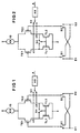
- the first input transistor TE1 and the first load transistor TL1 form a first input stage (an input stage for one of the operational amplifier input signals), and the second input transistor TE2 and the second load transistor TL2 form a second input stage (an input stage for the other of the operational amplifier input signals).
- Between the first input transistor TE1 and the first load transistor TL1 is a first node x5, and between the second input transistor TE2 and the second Load transistor TL2 is a second node x6.
- the input signals E1 and E2 are to the gate connections the input transistors TE1 and TE2, and the output signal is the signal output by the output stage.
- Said filter is in practice outside the operational amplifier be provided; basically it can but also be provided within the operational amplifier and there either the output stage input signal or that Filter output stage output signal or both signals.
Landscapes
- Engineering & Computer Science (AREA)
- Microelectronics & Electronic Packaging (AREA)
- Power Engineering (AREA)
- Physics & Mathematics (AREA)
- Nonlinear Science (AREA)
- Electromagnetism (AREA)
- General Physics & Mathematics (AREA)
- Radar, Positioning & Navigation (AREA)
- Automation & Control Theory (AREA)
- Amplifiers (AREA)
- Semiconductor Integrated Circuits (AREA)
- Control Of Electrical Variables (AREA)
Applications Claiming Priority (2)
| Application Number | Priority Date | Filing Date | Title |
|---|---|---|---|
| DE19735381A DE19735381C1 (de) | 1997-08-14 | 1997-08-14 | Bandgap-Referenzspannungsquelle und Verfahren zum Betreiben derselben |
| DE19735381 | 1998-08-14 |
Publications (3)
| Publication Number | Publication Date |
|---|---|
| EP0897143A2 true EP0897143A2 (fr) | 1999-02-17 |
| EP0897143A3 EP0897143A3 (fr) | 1999-05-06 |
| EP0897143B1 EP0897143B1 (fr) | 2001-10-04 |
Family
ID=7839050
Family Applications (1)
| Application Number | Title | Priority Date | Filing Date |
|---|---|---|---|
| EP98113265A Expired - Lifetime EP0897143B1 (fr) | 1997-08-14 | 1998-07-16 | Source de tension de référence du type Bandgap et procédé pour son opération |
Country Status (4)
| Country | Link |
|---|---|
| US (1) | US6014020A (fr) |
| EP (1) | EP0897143B1 (fr) |
| JP (1) | JPH11161355A (fr) |
| DE (2) | DE19735381C1 (fr) |
Families Citing this family (12)
| Publication number | Priority date | Publication date | Assignee | Title |
|---|---|---|---|---|
| DE19907177A1 (de) * | 1999-02-19 | 2000-08-31 | Siemens Ag | Verzögerungsschaltung |
| US6275098B1 (en) * | 1999-10-01 | 2001-08-14 | Lsi Logic Corporation | Digitally calibrated bandgap reference |
| DE10032257C2 (de) * | 2000-07-03 | 2003-06-05 | Infineon Technologies Ag | Verfahren und Vorrichtung zur offsetspannungsfreien Spannungsmessung und Einstellung der Spannung einer Referenzspannungsquelle einer integrierten Halbleiterschaltung |
| JP3519361B2 (ja) | 2000-11-07 | 2004-04-12 | Necエレクトロニクス株式会社 | バンドギャップレファレンス回路 |
| DE10057844A1 (de) | 2000-11-22 | 2002-06-06 | Infineon Technologies Ag | Verfahren zum Abgleichen eines BGR-Schaltkreises und BGR-Schaltkreis |
| US7091713B2 (en) * | 2004-04-30 | 2006-08-15 | Integration Associates Inc. | Method and circuit for generating a higher order compensated bandgap voltage |
| US7683701B2 (en) * | 2005-12-29 | 2010-03-23 | Cypress Semiconductor Corporation | Low power Bandgap reference circuit with increased accuracy and reduced area consumption |
| ITTO20090495A1 (it) * | 2009-06-30 | 2011-01-01 | St Microelectronics Srl | Circuito preamplificatore per un trasduttore acustico capacitivo di tipo microelettromeccanico |
| JP5461944B2 (ja) * | 2009-10-05 | 2014-04-02 | 凸版印刷株式会社 | バンドギャップリファレンス回路を備えるadコンバータ、並びに、バンドギャップリファレンス回路の調整方法 |
| US8169255B2 (en) * | 2010-08-31 | 2012-05-01 | National Tsing Hua University | Offset cancellation current mirror and operating method thereof |
| JP6073112B2 (ja) | 2012-11-13 | 2017-02-01 | ルネサスエレクトロニクス株式会社 | 基準電圧発生回路 |
| CN120582307B (zh) * | 2025-08-06 | 2026-01-02 | 敏业信息科技(上海)有限公司 | 脉动式预充电电路及其适用的电子设备 |
Family Cites Families (5)
| Publication number | Priority date | Publication date | Assignee | Title |
|---|---|---|---|---|
| GB2111223B (en) * | 1981-11-30 | 1985-07-10 | Ebauches Electroniques Sa | Voltage level detecting circuit |
| GB2254211A (en) * | 1990-06-07 | 1992-09-30 | Motorola Inc | Current mirrors |
| KR940003406B1 (ko) * | 1991-06-12 | 1994-04-21 | 삼성전자 주식회사 | 내부 전원전압 발생회로 |
| US5512817A (en) * | 1993-12-29 | 1996-04-30 | At&T Corp. | Bandgap voltage reference generator |
| US5563504A (en) * | 1994-05-09 | 1996-10-08 | Analog Devices, Inc. | Switching bandgap voltage reference |
-
1997
- 1997-08-14 DE DE19735381A patent/DE19735381C1/de not_active Expired - Fee Related
-
1998
- 1998-07-16 DE DE59801619T patent/DE59801619D1/de not_active Expired - Lifetime
- 1998-07-16 EP EP98113265A patent/EP0897143B1/fr not_active Expired - Lifetime
- 1998-08-12 JP JP10228303A patent/JPH11161355A/ja active Pending
- 1998-08-14 US US09/133,876 patent/US6014020A/en not_active Expired - Lifetime
Also Published As
| Publication number | Publication date |
|---|---|
| JPH11161355A (ja) | 1999-06-18 |
| DE19735381C1 (de) | 1999-01-14 |
| EP0897143A3 (fr) | 1999-05-06 |
| EP0897143B1 (fr) | 2001-10-04 |
| US6014020A (en) | 2000-01-11 |
| DE59801619D1 (de) | 2001-11-08 |
Similar Documents
| Publication | Publication Date | Title |
|---|---|---|
| DE2825882C2 (de) | Schaltungsanordnung zur Reduzierung niederfrequenter Störspannung und Offsetspannung bei einer Verstärkerschaltung | |
| DE69102813T2 (de) | Elektrisch steuerbare Oszillatorschaltung und eine damit ausgerüstete, elektrisch steuerbare Filterschaltung. | |
| DE69528234T2 (de) | Schaltung und Verfahren zur Erzeugung eines Taktsignals | |
| DE3872275T2 (de) | Cmos-referenzspannungsgeneratoreinrichtung. | |
| DE4034371C1 (fr) | ||
| DE1901804C3 (de) | Stabilisierter Differentialverstärker | |
| DE3713107C2 (de) | Schaltung zur Erzeugung von konstanten Spannungen in CMOS-Technologie | |
| EP0300560B1 (fr) | Circuit de comparison | |
| DE3420068C2 (fr) | ||
| EP0897143B1 (fr) | Source de tension de référence du type Bandgap et procédé pour son opération | |
| DE2254618B2 (de) | Integrierte spannungsregelschaltung | |
| DE2160432B2 (de) | Konstantspannungsschaltung | |
| DE68921136T2 (de) | Transistorverstärker für hohe Anstiegsgeschwindigkeiten und kapazitive Belastungen. | |
| DE1487396B2 (de) | Spannungsteilerschaltung | |
| DE69605571T2 (de) | Verstärkerschaltung | |
| DE69213213T2 (de) | Genauer MOS-Schwellenspannungsgenerator | |
| DE2631916C3 (de) | Auf einem Halbleiterchip aufgebauer Differenzverstärker aus MOS-Feldeffekttransistoren | |
| DE2905659B2 (de) | Gegentakt-Verstärkerkreis | |
| DE3873384T2 (de) | Steuerstromerzeugende differenzschaltung. | |
| EP0506174B1 (fr) | Dispositif à circuit intégré comprenant un amplificateur différentiel | |
| EP0360888A1 (fr) | Modulateur CMOS d'impulsions en durée | |
| EP0602466B1 (fr) | Régulateur de tension integré monolithique | |
| DE3243706C1 (de) | ECL-TTL-Signalpegelwandler | |
| DE60133068T2 (de) | Differentiell angeordnetes transistorpaar mit mitteln zur degeneration der transkonduktanz | |
| DE3546204C2 (de) | Monolithisch integrierte Signalverstärkersstufe mit hoher Ausgangsdynamik |
Legal Events
| Date | Code | Title | Description |
|---|---|---|---|
| PUAI | Public reference made under article 153(3) epc to a published international application that has entered the european phase |
Free format text: ORIGINAL CODE: 0009012 |
|
| AK | Designated contracting states |
Kind code of ref document: A2 Designated state(s): DE FR GB |
|
| AX | Request for extension of the european patent |
Free format text: AL;LT;LV;MK;RO;SI |
|
| PUAL | Search report despatched |
Free format text: ORIGINAL CODE: 0009013 |
|
| AK | Designated contracting states |
Kind code of ref document: A3 Designated state(s): AT BE CH CY DE DK ES FI FR GB GR IE IT LI LU MC NL PT SE |
|
| AX | Request for extension of the european patent |
Free format text: AL;LT;LV;MK;RO;SI |
|
| 17P | Request for examination filed |
Effective date: 19990607 |
|
| 17Q | First examination report despatched |
Effective date: 19991029 |
|
| AKX | Designation fees paid |
Free format text: DE FR GB |
|
| GRAG | Despatch of communication of intention to grant |
Free format text: ORIGINAL CODE: EPIDOS AGRA |
|
| GRAG | Despatch of communication of intention to grant |
Free format text: ORIGINAL CODE: EPIDOS AGRA |
|
| GRAH | Despatch of communication of intention to grant a patent |
Free format text: ORIGINAL CODE: EPIDOS IGRA |
|
| RAP1 | Party data changed (applicant data changed or rights of an application transferred) |
Owner name: INFINEON TECHNOLOGIES AG |
|
| GRAH | Despatch of communication of intention to grant a patent |
Free format text: ORIGINAL CODE: EPIDOS IGRA |
|
| GRAA | (expected) grant |
Free format text: ORIGINAL CODE: 0009210 |
|
| AK | Designated contracting states |
Kind code of ref document: B1 Designated state(s): DE FR GB |
|
| REF | Corresponds to: |
Ref document number: 59801619 Country of ref document: DE Date of ref document: 20011108 |
|
| REG | Reference to a national code |
Ref country code: GB Ref legal event code: IF02 |
|
| GBT | Gb: translation of ep patent filed (gb section 77(6)(a)/1977) |
Effective date: 20011217 |
|
| ET | Fr: translation filed | ||
| PLBE | No opposition filed within time limit |
Free format text: ORIGINAL CODE: 0009261 |
|
| STAA | Information on the status of an ep patent application or granted ep patent |
Free format text: STATUS: NO OPPOSITION FILED WITHIN TIME LIMIT |
|
| 26N | No opposition filed | ||
| REG | Reference to a national code |
Ref country code: FR Ref legal event code: TP |
|
| REG | Reference to a national code |
Ref country code: DE Ref legal event code: R081 Ref document number: 59801619 Country of ref document: DE Owner name: LANTIQ DEUTSCHLAND GMBH, DE Free format text: FORMER OWNER: INFINEON TECHNOLOGIES AG, 81669 MUENCHEN, DE Effective date: 20110325 |
|
| REG | Reference to a national code |
Ref country code: GB Ref legal event code: 732E Free format text: REGISTERED BETWEEN 20110602 AND 20110608 |
|
| REG | Reference to a national code |
Ref country code: GB Ref legal event code: 732E Free format text: REGISTERED BETWEEN 20110609 AND 20110615 |
|
| PGFP | Annual fee paid to national office [announced via postgrant information from national office to epo] |
Ref country code: FR Payment date: 20110729 Year of fee payment: 14 |
|
| PGFP | Annual fee paid to national office [announced via postgrant information from national office to epo] |
Ref country code: GB Payment date: 20110721 Year of fee payment: 14 Ref country code: DE Payment date: 20110722 Year of fee payment: 14 |
|
| GBPC | Gb: european patent ceased through non-payment of renewal fee |
Effective date: 20120716 |
|
| REG | Reference to a national code |
Ref country code: FR Ref legal event code: ST Effective date: 20130329 |
|
| PG25 | Lapsed in a contracting state [announced via postgrant information from national office to epo] |
Ref country code: FR Free format text: LAPSE BECAUSE OF NON-PAYMENT OF DUE FEES Effective date: 20120731 Ref country code: DE Free format text: LAPSE BECAUSE OF NON-PAYMENT OF DUE FEES Effective date: 20130201 Ref country code: GB Free format text: LAPSE BECAUSE OF NON-PAYMENT OF DUE FEES Effective date: 20120716 |
|
| REG | Reference to a national code |
Ref country code: DE Ref legal event code: R119 Ref document number: 59801619 Country of ref document: DE Effective date: 20130201 |