EP0897554B1 - Optische taktteilung - Google Patents
Optische taktteilung Download PDFInfo
- Publication number
- EP0897554B1 EP0897554B1 EP97918268A EP97918268A EP0897554B1 EP 0897554 B1 EP0897554 B1 EP 0897554B1 EP 97918268 A EP97918268 A EP 97918268A EP 97918268 A EP97918268 A EP 97918268A EP 0897554 B1 EP0897554 B1 EP 0897554B1
- Authority
- EP
- European Patent Office
- Prior art keywords
- gate
- optical
- linear
- output port
- output
- Prior art date
- Legal status (The legal status is an assumption and is not a legal conclusion. Google has not performed a legal analysis and makes no representation as to the accuracy of the status listed.)
- Expired - Lifetime
Links
Images




Classifications
-
- G—PHYSICS
- G02—OPTICS
- G02F—OPTICAL DEVICES OR ARRANGEMENTS FOR THE CONTROL OF LIGHT BY MODIFICATION OF THE OPTICAL PROPERTIES OF THE MEDIA OF THE ELEMENTS INVOLVED THEREIN; NON-LINEAR OPTICS; FREQUENCY-CHANGING OF LIGHT; OPTICAL LOGIC ELEMENTS; OPTICAL ANALOGUE/DIGITAL CONVERTERS
- G02F1/00—Devices or arrangements for the control of the intensity, colour, phase, polarisation or direction of light arriving from an independent light source, e.g. switching, gating or modulating; Non-linear optics
- G02F1/35—Non-linear optics
- G02F1/3515—All-optical modulation, gating, switching, e.g. control of a light beam by another light beam
- G02F1/3517—All-optical modulation, gating, switching, e.g. control of a light beam by another light beam using an interferometer
-
- H—ELECTRICITY
- H04—ELECTRIC COMMUNICATION TECHNIQUE
- H04J—MULTIPLEX COMMUNICATION
- H04J14/00—Optical multiplex systems
- H04J14/08—Time-division multiplex systems
-
- H—ELECTRICITY
- H04—ELECTRIC COMMUNICATION TECHNIQUE
- H04L—TRANSMISSION OF DIGITAL INFORMATION, e.g. TELEGRAPHIC COMMUNICATION
- H04L7/00—Arrangements for synchronising receiver with transmitter
- H04L7/0075—Arrangements for synchronising receiver with transmitter with photonic or optical means
-
- G—PHYSICS
- G02—OPTICS
- G02F—OPTICAL DEVICES OR ARRANGEMENTS FOR THE CONTROL OF LIGHT BY MODIFICATION OF THE OPTICAL PROPERTIES OF THE MEDIA OF THE ELEMENTS INVOLVED THEREIN; NON-LINEAR OPTICS; FREQUENCY-CHANGING OF LIGHT; OPTICAL LOGIC ELEMENTS; OPTICAL ANALOGUE/DIGITAL CONVERTERS
- G02F1/00—Devices or arrangements for the control of the intensity, colour, phase, polarisation or direction of light arriving from an independent light source, e.g. switching, gating or modulating; Non-linear optics
- G02F1/35—Non-linear optics
- G02F1/3515—All-optical modulation, gating, switching, e.g. control of a light beam by another light beam
- G02F1/3517—All-optical modulation, gating, switching, e.g. control of a light beam by another light beam using an interferometer
- G02F1/3519—All-optical modulation, gating, switching, e.g. control of a light beam by another light beam using an interferometer of Sagnac type, i.e. nonlinear optical loop mirror [NOLM]
-
- H—ELECTRICITY
- H01—ELECTRIC ELEMENTS
- H01S—DEVICES USING THE PROCESS OF LIGHT AMPLIFICATION BY STIMULATED EMISSION OF RADIATION [LASER] TO AMPLIFY OR GENERATE LIGHT; DEVICES USING STIMULATED EMISSION OF ELECTROMAGNETIC RADIATION IN WAVE RANGES OTHER THAN OPTICAL
- H01S5/00—Semiconductor lasers
- H01S5/50—Amplifier structures not provided for in groups H01S5/02 - H01S5/30
Definitions
- the present invention relates to the clock division of an optical signal.
- a clock signal at less than the full bit rate of the data stream may be needed in the operation of a demultiplexer to select one or more time channels.
- clock division when clock division has been required, this has commonly been carried out by tapping off part of the optical signal stream, detecting the signal to produce a corresponding timing wave in the electrical domain, and then dividing down the clock rate using conventional electronic clock-division circuits.
- a local optical source controlled by the electrical clock signal has to be used to take the divided signal back into the optical domain. Not only does this add undesirably to the cost and complexity of the relevant circuits, but the need for processing in the electrical domain severely limits the bit rates at which the circuit is capable of operating.
- the effect of driving the laser with data channels is to produce a clock pattern with a "1" in each of the active channel timeslots, and a "0" elsewhere.
- the data signal passes on to an output port.
- the clock pattern which may have a different bit pattern and is at a different wavelength to the data signal, is fed back as a control signal to the ultra-fast gate.
- the present invention adopts an approach to clock-division which allows the function to be carried out entirely in the optical domain, using a relatively simple method which is well-adapted for implementation using integrated fabrication and which overcomes the disadvantages of the prior art circuits discussed above.
- An all-optical non-linear gate is used. Optical feedback is provided from the output of the gate to a control input of a non-linear element. With the gate configured in this manner, it is found that when an optical signal stream is applied at its input, then a signal at a divided clock rate is present at the output of the gate.
- the optical signal stream is applied to an interferometric non-linear optical gate.
- This gate may comprise a non-linear loop mirror (NOLM) and more preferably an NOLM incorporating a semiconductor optical amplifier as its non-linear element.
- NOLM non-linear loop mirror
- other interferometric structures such as a Mach Zehnder interferometer, may be used.
- a non-linear interferometer and particularly an NOLM in a TOAD (TeraHertz Optically Asymmetric Demultiplexer) configuration with a semiconductor optical amplifier (SOA) as the phase switching element.
- SOA semiconductor optical amplifier
- Such a device has the advantages of low switching energy and is capable of operating rates approaching 100GHz.
- the use of a TOAD configuration has the further important advantage that the total delay time over the feedback path can be made as short as the bit period, even when the bit period may be as little as a few 10's of picoseconds.
- a further advantage of this preferred configuration is that the dynamics of the SOA support the clock division function.
- the delay period associated with the optical feedback path is equal to the period between bits in the optical signal stream.
- the method may include an initial phase of programming the gate to carry out clock division by inputting to the gate a block of pulses having a predetermined bit-pattern and of sufficient length to fill both the gate and the feedback path.
- the circuit may include an SOA having a response time such that the circuit exhibits spontaneous clock division.
- the method includes inducing spontaneous clock division in the non-linear gate by driving the semiconductor optical amplifier with the optical signal stream at a bit rate generally corresponding to the e -1 recovery rate of the semiconductor optical amplifier.
- the clock division circuit may comprise a plurality of stages each with its own respective non-linear gate, n such stages being cascaded in series to provide an output divided by 2 n .
- the present invention also encompasses a multiplexer or demultiplexer incorporating a clock division circuit in accordance with one or more of the preceding aspects of the invention.
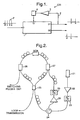
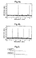
- a clock division circuit CT1 comprises a non-linear optical gate 1.
- the gate has an optical input I at which it receives an optical signal stream.
- the gate 1 has two optical outputs O1, O2. One of these outputs O1 is connected via an optical feedback path 2 to a control input G for the gate.
- the feedback path may include an optical amplifier 3 and filter 4.
- the optical gate 1 which may, for example, comprise an SOA in a fibre loop mirror as further described below, directs a signal received to the input I to one or other of the two output O1, O2 depending upon the presence or absence of a control signal at the input G. If the total delay time for transit through the gate and around the feedback path back to the input G is equal to the period p between successive bits, then the gate operates as follows to provide a divided clock signal. Assuming that the gate 1 is initially configured to switch pulses straight through to output 01, then the first pulse (labelled a in the Figure) output from 01 passes via the feedback path 2 to the control input G. Accordingly when the next pulse b arrives at the input, a control pulse is present at the control input G and so the pulse is switched to the second output 02.
- the output at O2 comprises a pulse stream at half the bit rate of the input pulse stream.
- the gate may still be programmed to effect clock division.
- Figure 5 shows an example of the signal used to initialise the circuit in the case where the total delay associated with the feedback path is equivalent to five bit periods.
- the upper sequence shows the input to the circuit, and the lower sequence is the output from the circuit.
- the lower sequence corresponds also to the control sequence fed back to the control input G.
- the gate is initially configured to switch pulses straight through to output O1.
- a frame five bits long, that is to say corresponding in length to the feedback path, is used to initialise the circuit.
- the first five input bits correspond to the sequence "10101". These are passed straight thorough to output 01, and are also fed into the feedback path.
- the input bit value like the preceding bit value, is "1".
- the first bit of the first frame, having bit value "1” reaches the control input G.
- the "1" in the sixth bit position is therefore switched to the other output 02.
- Bit value "0” therefore appears in the output from port 01.
- the value of the bit input in the seventh bit position is "1”.
- the second bit from the first frame reaches the control input.
- This has value "0” and accordingly the gate is set to transmit the seventh bit straight through to output 01.
- This pattern is repeated for successive bits, so that the overall output from 01 is in the form "10101". Therefore, even though the input to the gate is now a continuous stream of "1" 's the output continues to replicate the bit pattern applied in the initialisation phase, to provide a clock-divided output at half the bit rate.
- the circuit may be designed to operate with a feedback path more than one bit long, but without requiring initialisation in the manner of the immediately proceeding example. This is achieved by using a semiconductor non-linear element, and by exploiting the dynamics of the semiconductor by operating in a regime where spontaneous clock division occurs.
- the phenomena of clock division and other complex dynamic behaviour are due to the finite lifetime of semiconductor optical amplifiers (typically around 300ps) combined with the effect of feedback as a memory.
- the signal input to the circuit has a repetition rate less than the natural recovery rate of the SOA, then, without initial programming as described above, "block" behaviour is observed, and there is no pulse-to-pulse interaction since the gain of the amplifier recovers fully between pulses.
- the pulse separation become comparable to the amplifier lifetime, there is interaction between pulses since the phase shift experienced by any pulse depends on the pattern of the previous few pulses. In such a system with feedback, it is the memory of the initial start up sequence which affects subsequent pulses.
- the inventors have carried out numerical modelling of this system which confirms the effects described above, and which also predicts a period-doubling route to chaos for the system as the pulse power varies.
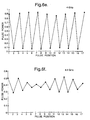
- Figures 6a to 6f show the results of numerical modelling of the system.
- Figure 6a shows the behaviour of the system when the input pulse stream has a repetition rate of 1.5GHz.
- the amplifier e -1 recovery period is 0.3ns.
- the separation between pulses is significantly greater than the recovery time, and so, in the absence of bit-to-bit interaction, the output is the form of blocks having a period corresponding to the delay length of the feedback path.
- the bit rate is increased, and so the bit separation is decreased, interaction between successive pulses begins to take place.
- Figure 6b shows the onset of this.
- the amplifier has not yet fully recovered from the marked decrease in carrier population associated with pulse 3. Accordingly the level of pulse 4 is diminished by comparison with pulse 3 and the succeeding pulses.
- Figure 6c shows that at 2.8GHz, the interaction between successive bits has resulted in spontaneous clock division. Instead of the entire block being switched and output, only alternate pulses are switched.
- the critical parameter in producing the clock-division behaviour is the ratio of the pulse rate to the amplifier e -1 recovery rate.
- these rates should be substantially equal, although, as illustrated in the example above, the precise ratio is not critical, and clock division will occur over a range of values for this ratio provided that the recovery rate and pulse rate are generally comparable. For example, as seen above, clock division may continue until the pulse rate differs from the e -1 recovery rate by more than 30%.
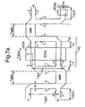
- Figures 7a and 7b illustrate an embodiment of the first circuit described above, that is a circuit having a short feedback path equal in length to a single bit period.
- the non-linear gate is an interferometric device using an integrated Mach-Zehnder structure.
- the circuit is formed in an III-V semiconductor substrate, which in this example is indium phosphide.
- Waveguides defining the paths for the optical signals are formed using ridge-waveguide structures.
- the Mach-Zehnder portion MZ comprises two arms offset by a length L SW which determines the length of the switching window.
- Semiconductor optical amplifiers SOA1 are integrated with each of the two arms. The SOA in each arm is individually controllable.
- an output coupler OC which is a multimode interference coupler of the type described by the paper by Soldano et al, "Planar Monomode Optical Couplers Based on Multimode Interference Effects", Journal of Lightwave Technology, 10, No. 12, December 1992, pp1843-1850.
- the feedback signal to the MZ gate is provided by a mirror formed by providing a reflective coating on the facet of the waveguide at the output port 04.
- a further amplifier SOA2 in the arm going to output port 04 amplifies the reflected signal which is then fed back to the amplifier SOA1 in the Mach-Zehnder portion MZ.
- the reflected signal acts as a control input to determine the state of SOA1.
- the structure may use a combination of deep and shallow-etched passive waveguides, with tapers formed in different regions of the waveguides for mode conversion.
- L TOT L OUT +L SW +L MMI + L F + L b +1 ⁇ 2 (L a +L b ).
- L TOT is approximately 900 ⁇ m which at a refractive index of 3.5 corresponds to a delay of 10 ps. This in turn corresponds to a single-bit delay at a bit rate of 100GHz.
- Figure 7b is a cross section through the line XX in Figure 7a. It shows part of the waveguide in the upper arm of the MZ portion, including part of the SOA.
- the SOA is a multiple quantum well (MQW) device, evanescently coupled to the waveguide layer.
- the waveguide layer is formed as a InGaAsP quaternary layer.
- An alternative SOA suitable for use as the non-linear element in the circuit of Figure 2 is a large spot size amplifier.
- the use of a large spot size allows easier and more efficient coupling of input and output beams from optical fibres.
- the large spot size amplifier also has angled facets which prevent lasing from occuring.
- the large spot size amplifier is described in A E Kelly, I F Lealman, L J Rivers, S D Perrin and Mark Silver, "Polarisation insensitive, 25dB gain semiconductor laser amplifier without antireflection coatings", Electronic Letters, vol 32, no.
- a further alternative amplifier, suitable for use as the non-linear element in both hybrid and integrated embodiments of the invention is a larger bandgap SLA (semiconductor laser amplifier).
- the alpha factor that is the ratio of the phase change to the amplitude change of a signal in the amplifier, is a strong function of the wavelength of the signal. The value of alpha increases asymptotically at the band edge.
- a large alpha factor is desirable for TOAD operation. Using a device with a large bandgap brings the operating wavelengths, e.g. 1547 nm and 1536 nm closer to the band edge and hence gives a larger alpha. The band edge is more clearly defined in a MQW device.
- the optical amplifier is a 7 well MQW device.
- the well is formed of unstrained InGaAs and the barrier layer is 1 % tensile-strained InGaAs. This has a photoluminescence wavelength of 1.553 microns and this wavelength broadly corresponds to the band edge.
- Figure 8 shows a second example of a circuit suitable for use with a feedback delay of one bit period, although it may also be used with a feedback delay of more than one bit period through the use of an initial programming phase as described above.
- the non-linear gate comprises a saturable absorber 82 in a laser cavity 81 including a semiconductor gain medium 83.
- the saturable absorber 82 may be, for example, ion-implanted InGaAsP and the whole device may be formed as an integrated semiconductor structure.
- one of the cavity mirrors of the laser is partially reflective and so both provides an output port, and also reflects light back into the saturable absorber in order to provide the feedback path.
- the other mirror defining the cavity is in this example, a reflective grating structure, which serves also to tune the cavity to a specific wavelength.
- the saturable absorber provides an intensity-dependent non-linearity with a response time which is slow compared to the bit separation.
- the response time is typically 10's or 100's of picoseconds.
- the feedback signal reflected back from the output optically biases the absorber so that it absorbs or transmits according to the value of the feedback signal.
- the amplifier 83 which in this example is formed integrally with the absorber, provides amplification for the signal in the feedback path.
- FIG. 2 shows a further embodiment relevant to the second and third schemes outline above.
- the switch in this example is formed from a TOAD-configured fibre loop mirror.
- the optical source in this case is a jitter-suppressed gain-switched distributed feedback (DFB) laser 21 operating at 1.55 ⁇ m, and producing a 2.5GHz train of pulses of around 20ps duration.
- This pulse train passes throught a first erbium doped fibre amplifier 22 and a filter 23.
- the pulse train is injected after amplification and filtering into the fibre loop mirror.
- An SOA is positioned in the loop and is spatially offset from the loop centre by around 3cm to give a switching window of around 150ps.
- the loop includes a 50:50 fibre coupler 25.
- Two polarisation selective fibre couplers 26,27 are used in the loop to introduce and reject the orthogonally polarised switching pulses. These pulses then act as switching pulses for the SOA.
- the mean power in the pulse train for switching is around 2.5mW at 2.5GHz corresponding to around 1pJ per pulse. Since the fibre lengths are fixed, the relative arrival time of the switching pulses at the SOA with respect to pulses in the loop can be varied by adjusting the repetition rate of the source. The repetition rate is also used to vary the total number of pulses in the feedback loop. Pulses reflected by the loop mirror in its linear mode of operation are amplified, polarisation rotated and fed back into the loop as switching pulses.
- An optical circulator 24 is used to select the reflected pulses which are then amplified by a second erbium doped fibre amplifier 28 and filtered by filter 29.
- Fibre polarisation controllers are used to define the polarisation state of the pulses in the various parts of the circuit.
- FIG 3 shows the temporal output of the input pulse train (a) and the loop output (b) when the feedback path contains an odd number of pulses.
- the clock division operation is clearly seen.
- the extinction ratio of the output is around 15dB which corresponds to the extinction of the loop, and the temporal output is extremely stable over several hours.
- the corresponding microwave spectra of the pulse trains are shown in Figures 4a and 4b.
- the clock-divided spectrum contains extremely narrow resonance's at half the frequency of the input pulse train, which indicates that the clock division pattern is a pure divide-by-two operation. When the number of pulses in the feedback path is even, more complicated behaviour is observed, and the microwave spectrum becomes more structured. Stable clock division is only achieved with an odd number of pulses, as explained previously.
- the circuit of Figure 2 exhibits spontaneous clock division, as discussed above. However, the circuit may also be used at other clock rates where clock division does not occur spontaneously. It is then necessary to introduce an initial programming phase in which, as already discussed, a programming frame of length equal to the delay path and having the form "101010..." is used to initialise the circuit.
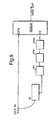
- FIG. 9 A further extension of the present invention is shown schematically in Figure 9.
- a series of n clock division circuits 9li-iii generally corresponding to that of Figure 1 are used in series to provide an overall division by 2 n .
- n equals 3, so that the clock rate of the output pulse stream is one eighth of that of the input bit rate.
- This example shows the clock division circuit used in the context of an eight-channel demultiplexer.
- Clock division is an important function for applications such as demultiplexing, since a clock rate which is a submultiple of the line rate is usually required, whereas in some all-optical clock recovery schemes, the recovered clock is at the original line rate.
- the clock recovery rate stage 92 shown in the figure may, for example, be that described in the paper by Patrick D M and Manning R J "20Gbit/s All-optical Clock Recovery Using Semiconductor Non-linearity", Electron. Lett. 1994, 30, pp151-152.
- the SOA lifetime may be controlled to establish the correct conditions for spontaneous clock division using appropriate electrical bias, and also optionally the injection of an optical bias signal as described in the papers by Manning et al: "Enhanced Recovery Rates in Semiconductor Amplifiers Using Optical Pumping", Electron. Lett. 1994, 30, pp787-788 and "Recovery Rates in Semiconductor Laser Amplifiers: Optical and Electrical Bias Dependencies", Electron. Lett. 1994, 30, pp1233-1234.
Landscapes
- Physics & Mathematics (AREA)
- Nonlinear Science (AREA)
- Optics & Photonics (AREA)
- Engineering & Computer Science (AREA)
- Computer Networks & Wireless Communication (AREA)
- Signal Processing (AREA)
- General Physics & Mathematics (AREA)
- Optical Communication System (AREA)
- Semiconductor Lasers (AREA)
- Optical Modulation, Optical Deflection, Nonlinear Optics, Optical Demodulation, Optical Logic Elements (AREA)
- Synchronisation In Digital Transmission Systems (AREA)
Claims (18)
- Verfahren zum Ableiten eines Taktsignals mit einer geteilten Taktfrequenz aus einem optischen Signalstrom mit einer höheren Taktfrequenz, das ein vollständig optisches nichtlineares Gatters (1) mit einem nichtlinearen Element verwendet, wobei der optische Signalstrom aus einer Folge von optischen Pulsen mit festgelegter Periodendauer eines Bits besteht, bei dem das vollständig optische nichtlineare Gatter (1) einen Dateneingang (I) zum Eingeben von optischen Datenpulsen, einen Steuereingang (G) zum Empfangen von optischen Steuerpulsen und wenigstens einen ersten Ausgangsanschluss (O1) zum Ausgeben von wenigstens einigen der optischen Datenpulse hat, wobei das Gatter (1) derart eingerichtet ist, dass, wenn ein Datenpuls an dem Dateneingang (I) anliegt, die Fähigkeit des Gatters, einen entsprechenden Datenpuls an dem ersten Ausgangsanschluss (O1) zu erzeugen, von der Anwesenheit oder Abwesenheit eines Steuerpulses an dem Steuereingang (G) abhängig ist, und wenn kein Datenpuls an dem Dateneingang (I) anliegt, die Abwesenheit des Datenpulses verursacht, dass das Gatter keinen entsprechenden Datenpuls an dem ersten Ausgangsanschluss (O1) erzeugt, wobei das Verfahren die folgenden Schritte umfasst:Anlegen des optischen Signalstroms an den Dateneingang (I) des Gatters (1); undAnlegen von optischen Daten, die aus dem ersten Ausgangsanschluss des Gatters (1) ausgegeben werden, an den Steuereingang des Gatters (1) über einen optischen Rückkopplungspfad (2, 3, 4), mit dem eine Verzögerungsdauer verbunden ist, wobei die Verzögerungsdauer gleich einer ungeraden Anzahl von Bitperioden ist, sodass ein Signal mit der geteilten Taktfrequenz aus dem ersten Ausgangsanschluss (O1) des Gatters und/oder einem anderen Ausgangsanschluss (02) des Gatters ausgegeben wird.
- Verfahren nach Anspruch 1, bei dem das Gatter (1) einen zweiten Ausgangsanschluss (02) enthält, wobei das Gatter derart eingerichtet ist, dass, wenn ein optischer Datenpuls an dem Dateneingang (I) vorhanden ist, ein entsprechender Datenpuls entweder an dem ersten Ausgangsanschluss (O1) oder an dem zweiten Ausgangsanschluss (02) in Abhängigkeit von der Anwesenheit oder Abwesenheit eines Steuerpulses an dem Steuereingang (G) erzeugt wird, und bei dem ein Signal mit der geteilten Taktfrequenz an dem zweiten Ausgangsanschluss (02) des Gatters (1) erzeugt wird.
- Verfahren nach Anspruch 1 oder 2, bei dem der optische Strom an ein interferometrisches nichtlineares Gatter mit einem nichtlinearen Sagnac-Interferometer angelegt wird.
- Verfahren nach Anspruch 3, bei dem das nichtlineare Element ein optischer Halbleiterverstärker innerhalb des Sagnac-Interferometers ist.
- Verfahren nach Anspruch 1 oder 2, bei dem der optische Signalstrom an einen Eingangsanschluss eines integrierten Mach-Zehnder-Interferometers angelegt ist, und bei dem das nichtlineare Element ein optischer Halbleiterverstärker (SOA, Semiconductor Optical Amplifier) ist, der in einem Arm des integrierten Mach-Zehnder-Interferometers angeordnet ist.
- Verfahren nach einem der vorangehenden Ansprüche, bei dem die Verzögerungsdauer, die mit dem optischen Rückkopplungspfad (2, 3, 4) verbunden ist, gleich der Periodendauer (p) zwischen Bits in dem optischen Signalstrom ist.
- Verfahren nach einem der Ansprüche 1 bis 5, das weiter eine Anfangsphase der Programmierung des Gatters umfasst, um die Taktteilung auszuführen, indem in das Gatter ein Block von Pulsen mit einem vordefinierten Bitmuster und ausreichender Länge eingegeben wird, um sowohl das Gatter als auch den optischen Rückkopplungspfad zu füllen.
- Verfahren nach einem der Ansprüche 1 bis 3, bei dem das nichtlineare Element ein optischer Halbleiterverstärker (SOA) ist, und bei dem das Verfahren das Herbeiführen von spontaner Taktteilung in dem nichtlinearen Gatter umfasst, indem der optische Halbleiterverstärker mit dem optischen Signalstrom mit einer Bitrate angesteuert wird, die im allgemeinen der e-1-exponentiellen Wiedergewinnungsrate des optischen Halbleiterverstärkers entspricht.
- Verfahren nach einem der vorangehenden Ansprüche, das weiter das Anlegen des optischen Signals mit der geteilten Taktfrequenz aus dem Gatter an den Eingang eines weiteren vollständig optischen nichtlinearen Gatters, das Rückkoppeln eines optischen Signals von einem Ausgang des weiteren Gatters zu einem nichtlinearen Element des weiteren Gatters und das Ausgeben eines optischen Signals aus dem weiteren Gatter mit einer weiter heruntergeteilten Taktfrequenz umfasst.
- Verfahren nach Anspruch 1, bei dem der Signalstrom in den optischen Resonanzraum eines Lasers eingebracht wird, der einen sättigbaren Absorber enthält, der dazu eingerichtet ist, als das nichtlineare Element zu arbeiten.
- Taktteilungsschaltkreis zur Ableitung eines Taktsignals mit einer geteilten Taktfrequenz aus einem optischen Taktstrom mit einer höheren Taktfrequenz als die geteilte Taktfrequenz, wobei der optische Signalstrom von einer Folge von optischen Pulsen mit einer festgelegten Periodendauer der Bits gebildet wird, wobei der Taktteilungsschaltkreis ein vollständig optisches nichtlineares Gatter (1) mit einem nichtlinearen Element, einem optischen Rückkopplungspfad (2, 3, 4), mit dem eine Verzögerungsdauer verbunden ist, umfasst, wobei das Gatter (1) einen Dateneingang (I) zum Eingeben von optischen Datenpulsen, einen Steuereingang (G) zum Empfangen von optischen Steuerpulsen und wenigstens einen ersten Datenausgangsanschluss (O1) zum Ausgeben von wenigstens einigen der optischen Datenpulse umfasst, wobei das Gatter derart eingerichtet ist, dass, wenn ein Datenpuls an dem Dateneingang (I) vorhanden ist, die Fähigkeit des Gatters, einen entsprechenden Datenpuls an dem ersten Ausgangsanschluss (O1) zu erzeugen, von der Anwesenheit oder Abwesenheit eines Steuerpulsen an dem Steuereingang (G) abhängt, und wenn kein Datenpuls an dem Dateneingang (I) vorhanden ist, die Abwesenheit des Datenpulses das Gatter veranlasst, keinen entsprechenden Datenpuls an dem ersten Ausgangsanschluss (O1) zu erzeugen, wobei der optische Rückkopplungspfad (2, 3, 4) zwischen dem ersten Ausgangsanschluss des Gatters (1) und dem Steuereingang des Gatters (1) angeordnet ist, sodass Daten, die aus dem ersten Ausgangsanschluss ausgegeben werden, über den Rückkopplungspfad an den Steuereingang des Gatters (1) angelegt werden, wobei die Verzögerungsdauer, die mit dem Rückkopplungspfad verbunden ist, gleich einer ungeraden Anzahl von Bitperioden ist, sodass, wenn ein optischer Signalstrom an den Dateneingang (I) des Gatters (1) angelegt wird, ein Signal mit der geteilten Taktfrequenz an dem ersten Ausgangsanschluss (O1) des Gatters (1) und/oder einem anderen Ausgangsanschluss (O2) des Gatters (I) erzeugt wird.
- Taktteilungsschaltkreis nach Anspruch 11, bei dem das Gatter (1) einen interferometrisches nichtlineares optisches Gatter ist.
- Taktteilungsschaltkreis nach Anspruch 12, bei dem das nichtlineare optische Gatter (1) ein Sagnac-Interferometer ist.
- Taktteilungsschaltkreis nach einem der Ansprüche 11 bis 13., bei dem das nichtlineare Element des Gatters ein optischer Halbleiterverstärker (SOA) ist.
- Taktteilungsschaltkreis nach Anspruch 14, bei dem das nichtlineare Gatter (1) ein integriertes Mach-Zehnder-Interferometer (MZ) umfasst, und bei dem das nichtlineare Element ein optischer Halbleiterverstärker (SOA1) ist, der in einem Arm des integrierten Mach-Zehnder-Interferometers angeordnet ist.
- Taktteilungsschaltkreis nach einem der Ansprüche 11 bis 15, der wenigstens ein weiteres vollständig optisches nichtlineares Gatter enthält, das mit seinem Eingang an den Ausgang des ersten optischen Gatters angeschlossen ist, und der einen Rückkopplungspfad von dem Ausgang des weiteren Gatters zu dem nichtlinearen Element des weiteren Gatters enthält, wobei das weitere Gatter bei der Verwendung ein optisches Signal mit einer weiter heruntergeteilten Taktfrequenz ausgibt.
- Taktteilungsschaltkreis nach Anspruch 11, bei dem das vollständig optische nichtlineare Gatter ein Laser ist und als nichtlineares Element einen sättigbaren Absorber enthält, der in dem optischen Resonanzraum des Lasers angeordnet ist.
- Zeit-Multiplexer oder -Demultiplexer mit einem Taktteilungsschaltkreis (91 i-iii) nach einem der vorangehenden Ansprüche.
Priority Applications (1)
| Application Number | Priority Date | Filing Date | Title |
|---|---|---|---|
| EP97918268A EP0897554B1 (de) | 1996-05-08 | 1997-04-30 | Optische taktteilung |
Applications Claiming Priority (4)
| Application Number | Priority Date | Filing Date | Title |
|---|---|---|---|
| EP96303216 | 1996-05-08 | ||
| EP96303216 | 1996-05-08 | ||
| EP97918268A EP0897554B1 (de) | 1996-05-08 | 1997-04-30 | Optische taktteilung |
| PCT/GB1997/001178 WO1997042543A1 (en) | 1996-05-08 | 1997-04-30 | Optical clock division |
Publications (2)
| Publication Number | Publication Date |
|---|---|
| EP0897554A1 EP0897554A1 (de) | 1999-02-24 |
| EP0897554B1 true EP0897554B1 (de) | 2005-11-09 |
Family
ID=8224925
Family Applications (1)
| Application Number | Title | Priority Date | Filing Date |
|---|---|---|---|
| EP97918268A Expired - Lifetime EP0897554B1 (de) | 1996-05-08 | 1997-04-30 | Optische taktteilung |
Country Status (8)
| Country | Link |
|---|---|
| US (1) | US6344913B1 (de) |
| EP (1) | EP0897554B1 (de) |
| JP (1) | JP2000511648A (de) |
| CN (1) | CN1218558A (de) |
| AU (1) | AU731322B2 (de) |
| CA (1) | CA2253485C (de) |
| DE (1) | DE69734578T2 (de) |
| WO (1) | WO1997042543A1 (de) |
Families Citing this family (3)
| Publication number | Priority date | Publication date | Assignee | Title |
|---|---|---|---|---|
| US6671426B2 (en) * | 2001-03-19 | 2003-12-30 | General Instrument Corporation | Monolithic integrated terahertz optical asymmetric demultiplexer |
| JP2005348127A (ja) * | 2004-06-03 | 2005-12-15 | Yokogawa Electric Corp | 光クロック信号抽出装置 |
| US11588302B2 (en) * | 2019-06-21 | 2023-02-21 | Seagate Technology Llc | Optical switches |
Family Cites Families (12)
| Publication number | Priority date | Publication date | Assignee | Title |
|---|---|---|---|---|
| US4980891A (en) * | 1989-12-22 | 1990-12-25 | Bell Communications Research, Inc. | Clocked optical regenerator and other optoelectronic functional circuits |
| EP0567693A1 (de) * | 1992-04-27 | 1993-11-03 | BRITISH TELECOMMUNICATIONS public limited company | Optische Taktrückgewinnung |
| DK0723716T3 (da) * | 1993-10-11 | 1999-08-09 | British Telecomm | Optisk impulssekvensgenerator |
| CA2173237C (en) * | 1993-10-11 | 2000-04-18 | Robert John Manning | Optical switching device |
| US5959753A (en) * | 1994-01-25 | 1999-09-28 | The United States Of America As Represented By The Secretary Of The Navy | Ultra high bit rate all optical communication system |
| US5574588A (en) * | 1994-02-23 | 1996-11-12 | Nippon Telegraph And Telephone Corporation | Phase lock loop circuit using optical correlation detection |
| US5493433A (en) * | 1994-03-02 | 1996-02-20 | Trustees Of Princeton University | Terahertz optical asymmetric demultiplexer |
| US5999287A (en) * | 1994-12-23 | 1999-12-07 | British Telecommunications Public Limited Company | Node in optical TDM network |
| US5999293A (en) * | 1995-01-19 | 1999-12-07 | British Telecommunications Public Limited Company | Optical switch |
| DE69616211T2 (de) * | 1995-03-15 | 2002-06-27 | Koninklijke Philips Electronics N.V., Eindhoven | Einheit zur modulation einer optischen pulsreihe in übereinstimmung mit einem datensignal |
| DE19511819A1 (de) * | 1995-03-30 | 1996-10-02 | Sel Alcatel Ag | Vorrichtung zum Demultiplexen eines optischen Digitalsignals |
| US5940198A (en) * | 1995-12-22 | 1999-08-17 | U.S. Philips Corporation | Optical unit for synchronizing clock signals |
-
1997
- 1997-04-30 JP JP09539627A patent/JP2000511648A/ja active Pending
- 1997-04-30 AU AU26462/97A patent/AU731322B2/en not_active Ceased
- 1997-04-30 US US09/011,785 patent/US6344913B1/en not_active Expired - Lifetime
- 1997-04-30 DE DE69734578T patent/DE69734578T2/de not_active Expired - Fee Related
- 1997-04-30 EP EP97918268A patent/EP0897554B1/de not_active Expired - Lifetime
- 1997-04-30 CN CN97194509.8A patent/CN1218558A/zh active Pending
- 1997-04-30 WO PCT/GB1997/001178 patent/WO1997042543A1/en not_active Ceased
- 1997-04-30 CA CA002253485A patent/CA2253485C/en not_active Expired - Fee Related
Also Published As
| Publication number | Publication date |
|---|---|
| CA2253485A1 (en) | 1997-11-13 |
| DE69734578D1 (de) | 2005-12-15 |
| JP2000511648A (ja) | 2000-09-05 |
| CN1218558A (zh) | 1999-06-02 |
| DE69734578T2 (de) | 2006-07-20 |
| CA2253485C (en) | 2002-05-28 |
| US6344913B1 (en) | 2002-02-05 |
| EP0897554A1 (de) | 1999-02-24 |
| AU731322B2 (en) | 2001-03-29 |
| AU2646297A (en) | 1997-11-26 |
| WO1997042543A1 (en) | 1997-11-13 |
Similar Documents
| Publication | Publication Date | Title |
|---|---|---|
| Hess et al. | All-optical demultiplexing of 80 to 10 Gb/s signals with monolithic integrated high-performance Mach-Zehnder interferometer | |
| EP0723676B1 (de) | Optische schalteinrichtung | |
| US7031047B2 (en) | Intensity modulation of optical signals | |
| EP1170627B1 (de) | Optisches Tor und optischer Phasenmodulator | |
| US6925220B2 (en) | Optical switch using multimode interferometer, and optical demultiplexer | |
| Manning et al. | Wavelength dependence of switching contrast ratio of semiconductor optical amplifier-based nonlinear loop mirror | |
| US5796765A (en) | Optical pulse seqeunce generator | |
| CA2253485C (en) | Optical clock division | |
| EP1255157A1 (de) | Intensitätsmodulation eines optischen Signals | |
| Manning et al. | All-optical clock division using a semiconductor optical amplifier loop mirror with feedback | |
| Mikkelsen et al. | Wavelength conversion devices | |
| AU3613499A (en) | Optical communications network | |
| Eiselt et al. | SLALOM as high speed multiplexer/demultiplexer | |
| Zhu et al. | A novel all-optical switch: the wavelength recognizing switch | |
| Liu et al. | All-optical signal processing for optical packet switching networks | |
| Agrawal et al. | Semiconductor-laser-amplifier-based integrated interferometers for add/drop multiplexing in OTDM systems | |
| JP2007124026A (ja) | 光クロック信号抽出方法及び光クロック信号抽出装置 | |
| Nolting | All-optical signal processing devices for photonic networks: towards packet switching | |
| Phillips | OTDM network processing using all-optical and electro-optical devices | |
| Yiannopoulos et al. | A repetition rate upgrade from 10 to 40 GHz for laser sources | |
| Mathason et al. | All-optical multiwavelength switching for hybrid WDM/TDM demultiplexing and signal processing | |
| Xu | SOA-based photonic technologies for hybrid optical networks | |
| Wang et al. | 8x2. 5-Gb/s OTDM data demultiplexing using an SLALOM | |
| HK1010064B (en) | Optical switching device | |
| Lal et al. | 10Gbps Monolithically-Integrated Widely-Tunable Wavelength Converter Using Quantum Well Intermixing |
Legal Events
| Date | Code | Title | Description |
|---|---|---|---|
| PUAI | Public reference made under article 153(3) epc to a published international application that has entered the european phase |
Free format text: ORIGINAL CODE: 0009012 |
|
| 17P | Request for examination filed |
Effective date: 19981027 |
|
| AK | Designated contracting states |
Kind code of ref document: A1 Designated state(s): BE CH DE DK ES FI FR GB IE IT LI NL PT SE |
|
| 17Q | First examination report despatched |
Effective date: 19991206 |
|
| APBT | Appeal procedure closed |
Free format text: ORIGINAL CODE: EPIDOSNNOA9E |
|
| GRAP | Despatch of communication of intention to grant a patent |
Free format text: ORIGINAL CODE: EPIDOSNIGR1 |
|
| GRAS | Grant fee paid |
Free format text: ORIGINAL CODE: EPIDOSNIGR3 |
|
| GRAA | (expected) grant |
Free format text: ORIGINAL CODE: 0009210 |
|
| APAH | Appeal reference modified |
Free format text: ORIGINAL CODE: EPIDOSCREFNO |
|
| AK | Designated contracting states |
Kind code of ref document: B1 Designated state(s): BE CH DE DK ES FI FR GB IE IT LI NL PT SE |
|
| PG25 | Lapsed in a contracting state [announced via postgrant information from national office to epo] |
Ref country code: NL Free format text: LAPSE BECAUSE OF FAILURE TO SUBMIT A TRANSLATION OF THE DESCRIPTION OR TO PAY THE FEE WITHIN THE PRESCRIBED TIME-LIMIT Effective date: 20051109 Ref country code: LI Free format text: LAPSE BECAUSE OF FAILURE TO SUBMIT A TRANSLATION OF THE DESCRIPTION OR TO PAY THE FEE WITHIN THE PRESCRIBED TIME-LIMIT Effective date: 20051109 Ref country code: IT Free format text: LAPSE BECAUSE OF FAILURE TO SUBMIT A TRANSLATION OF THE DESCRIPTION OR TO PAY THE FEE WITHIN THE PRE;WARNING: LAPSES OF ITALIAN PATENTS WITH EFFECTIVE DATE BEFORE 2007 MAY HAVE OCCURRED AT ANY TIME BEFORE 2007. THE CORRECT EFFECTIVE DATE MAY BE DIFFERENT FROM THE ONE RECORDED.SCRIBED TIME-LIMIT Effective date: 20051109 Ref country code: FI Free format text: LAPSE BECAUSE OF FAILURE TO SUBMIT A TRANSLATION OF THE DESCRIPTION OR TO PAY THE FEE WITHIN THE PRESCRIBED TIME-LIMIT Effective date: 20051109 Ref country code: CH Free format text: LAPSE BECAUSE OF FAILURE TO SUBMIT A TRANSLATION OF THE DESCRIPTION OR TO PAY THE FEE WITHIN THE PRESCRIBED TIME-LIMIT Effective date: 20051109 Ref country code: BE Free format text: LAPSE BECAUSE OF FAILURE TO SUBMIT A TRANSLATION OF THE DESCRIPTION OR TO PAY THE FEE WITHIN THE PRESCRIBED TIME-LIMIT Effective date: 20051109 |
|
| REG | Reference to a national code |
Ref country code: GB Ref legal event code: FG4D |
|
| REG | Reference to a national code |
Ref country code: CH Ref legal event code: EP |
|
| REG | Reference to a national code |
Ref country code: IE Ref legal event code: FG4D |
|
| REF | Corresponds to: |
Ref document number: 69734578 Country of ref document: DE Date of ref document: 20051215 Kind code of ref document: P |
|
| PG25 | Lapsed in a contracting state [announced via postgrant information from national office to epo] |
Ref country code: SE Free format text: LAPSE BECAUSE OF FAILURE TO SUBMIT A TRANSLATION OF THE DESCRIPTION OR TO PAY THE FEE WITHIN THE PRESCRIBED TIME-LIMIT Effective date: 20060209 Ref country code: DK Free format text: LAPSE BECAUSE OF FAILURE TO SUBMIT A TRANSLATION OF THE DESCRIPTION OR TO PAY THE FEE WITHIN THE PRESCRIBED TIME-LIMIT Effective date: 20060209 |
|
| PG25 | Lapsed in a contracting state [announced via postgrant information from national office to epo] |
Ref country code: ES Free format text: LAPSE BECAUSE OF FAILURE TO SUBMIT A TRANSLATION OF THE DESCRIPTION OR TO PAY THE FEE WITHIN THE PRESCRIBED TIME-LIMIT Effective date: 20060220 |
|
| PG25 | Lapsed in a contracting state [announced via postgrant information from national office to epo] |
Ref country code: PT Free format text: LAPSE BECAUSE OF FAILURE TO SUBMIT A TRANSLATION OF THE DESCRIPTION OR TO PAY THE FEE WITHIN THE PRESCRIBED TIME-LIMIT Effective date: 20060410 |
|
| NLV1 | Nl: lapsed or annulled due to failure to fulfill the requirements of art. 29p and 29m of the patents act | ||
| PG25 | Lapsed in a contracting state [announced via postgrant information from national office to epo] |
Ref country code: IE Free format text: LAPSE BECAUSE OF NON-PAYMENT OF DUE FEES Effective date: 20060501 |
|
| REG | Reference to a national code |
Ref country code: CH Ref legal event code: PL |
|
| ET | Fr: translation filed | ||
| PLBE | No opposition filed within time limit |
Free format text: ORIGINAL CODE: 0009261 |
|
| STAA | Information on the status of an ep patent application or granted ep patent |
Free format text: STATUS: NO OPPOSITION FILED WITHIN TIME LIMIT |
|
| 26N | No opposition filed |
Effective date: 20060810 |
|
| REG | Reference to a national code |
Ref country code: IE Ref legal event code: MM4A |
|
| PGFP | Annual fee paid to national office [announced via postgrant information from national office to epo] |
Ref country code: GB Payment date: 20080320 Year of fee payment: 12 |
|
| PGFP | Annual fee paid to national office [announced via postgrant information from national office to epo] |
Ref country code: FR Payment date: 20080313 Year of fee payment: 12 Ref country code: DE Payment date: 20080320 Year of fee payment: 12 |
|
| GBPC | Gb: european patent ceased through non-payment of renewal fee |
Effective date: 20090430 |
|
| REG | Reference to a national code |
Ref country code: FR Ref legal event code: ST Effective date: 20091231 |
|
| PG25 | Lapsed in a contracting state [announced via postgrant information from national office to epo] |
Ref country code: DE Free format text: LAPSE BECAUSE OF NON-PAYMENT OF DUE FEES Effective date: 20091103 |
|
| PG25 | Lapsed in a contracting state [announced via postgrant information from national office to epo] |
Ref country code: GB Free format text: LAPSE BECAUSE OF NON-PAYMENT OF DUE FEES Effective date: 20090430 Ref country code: FR Free format text: LAPSE BECAUSE OF NON-PAYMENT OF DUE FEES Effective date: 20091222 |