EP0898294A2 - Kathodenstrahlröhre und Ablenkungsaberration-Kompensationsverfahren - Google Patents
Kathodenstrahlröhre und Ablenkungsaberration-Kompensationsverfahren Download PDFInfo
- Publication number
- EP0898294A2 EP0898294A2 EP98122128A EP98122128A EP0898294A2 EP 0898294 A2 EP0898294 A2 EP 0898294A2 EP 98122128 A EP98122128 A EP 98122128A EP 98122128 A EP98122128 A EP 98122128A EP 0898294 A2 EP0898294 A2 EP 0898294A2
- Authority
- EP
- European Patent Office
- Prior art keywords
- ray tube
- cathode ray
- deflection
- electron beam
- electrode
- Prior art date
- Legal status (The legal status is an assumption and is not a legal conclusion. Google has not performed a legal analysis and makes no representation as to the accuracy of the status listed.)
- Withdrawn
Links
- 230000004075 alteration Effects 0.000 title claims abstract description 308
- 238000000034 method Methods 0.000 title description 33
- 238000010894 electron beam technology Methods 0.000 claims abstract description 465
- 230000009471 action Effects 0.000 claims abstract description 72
- 230000008859 change Effects 0.000 claims abstract description 18
- 230000005684 electric field Effects 0.000 claims description 299
- 238000007493 shaping process Methods 0.000 claims description 7
- 206010010071 Coma Diseases 0.000 claims description 3
- 238000010586 diagram Methods 0.000 description 127
- 238000012937 correction Methods 0.000 description 35
- 230000004907 flux Effects 0.000 description 34
- 238000010276 construction Methods 0.000 description 33
- 230000001965 increasing effect Effects 0.000 description 32
- 238000009826 distribution Methods 0.000 description 29
- 230000000694 effects Effects 0.000 description 21
- 125000001475 halogen functional group Chemical group 0.000 description 18
- 230000003287 optical effect Effects 0.000 description 16
- 239000000696 magnetic material Substances 0.000 description 13
- 230000004323 axial length Effects 0.000 description 12
- 230000007246 mechanism Effects 0.000 description 11
- 206010073261 Ovarian theca cell tumour Diseases 0.000 description 10
- 208000001644 thecoma Diseases 0.000 description 10
- 230000002093 peripheral effect Effects 0.000 description 9
- 201000009310 astigmatism Diseases 0.000 description 7
- 230000006866 deterioration Effects 0.000 description 6
- 238000004519 manufacturing process Methods 0.000 description 6
- 238000004904 shortening Methods 0.000 description 6
- 230000010485 coping Effects 0.000 description 5
- 238000013461 design Methods 0.000 description 5
- 230000035515 penetration Effects 0.000 description 5
- 230000015556 catabolic process Effects 0.000 description 4
- 230000003247 decreasing effect Effects 0.000 description 4
- 239000000463 material Substances 0.000 description 4
- 240000000136 Scabiosa atropurpurea Species 0.000 description 3
- 238000006731 degradation reaction Methods 0.000 description 3
- 238000009413 insulation Methods 0.000 description 3
- OKTJSMMVPCPJKN-UHFFFAOYSA-N Carbon Chemical compound [C] OKTJSMMVPCPJKN-UHFFFAOYSA-N 0.000 description 2
- 230000001133 acceleration Effects 0.000 description 2
- 238000013459 approach Methods 0.000 description 2
- 230000003190 augmentative effect Effects 0.000 description 2
- 238000012790 confirmation Methods 0.000 description 2
- 229910002804 graphite Inorganic materials 0.000 description 2
- 239000010439 graphite Substances 0.000 description 2
- 238000010438 heat treatment Methods 0.000 description 2
- 238000009434 installation Methods 0.000 description 2
- 238000005259 measurement Methods 0.000 description 2
- 239000002184 metal Substances 0.000 description 2
- 238000003825 pressing Methods 0.000 description 2
- 230000001737 promoting effect Effects 0.000 description 2
- 230000000087 stabilizing effect Effects 0.000 description 2
- 230000001629 suppression Effects 0.000 description 2
- 241000226585 Antennaria plantaginifolia Species 0.000 description 1
- 230000008901 benefit Effects 0.000 description 1
- 230000015572 biosynthetic process Effects 0.000 description 1
- 230000001419 dependent effect Effects 0.000 description 1
- 230000002542 deteriorative effect Effects 0.000 description 1
- 239000000428 dust Substances 0.000 description 1
- 230000002708 enhancing effect Effects 0.000 description 1
- 230000006870 function Effects 0.000 description 1
- 230000006872 improvement Effects 0.000 description 1
- 238000011835 investigation Methods 0.000 description 1
- 230000013011 mating Effects 0.000 description 1
- 239000011368 organic material Substances 0.000 description 1
- 238000005192 partition Methods 0.000 description 1
- 230000000149 penetrating effect Effects 0.000 description 1
- 230000035699 permeability Effects 0.000 description 1
- 230000002028 premature Effects 0.000 description 1
- 230000002265 prevention Effects 0.000 description 1
- 230000008569 process Effects 0.000 description 1
- 238000003908 quality control method Methods 0.000 description 1
- 230000009467 reduction Effects 0.000 description 1
- 239000004065 semiconductor Substances 0.000 description 1
- 230000006641 stabilisation Effects 0.000 description 1
- 238000011105 stabilization Methods 0.000 description 1
- 239000000126 substance Substances 0.000 description 1
- 238000012546 transfer Methods 0.000 description 1
- 238000005303 weighing Methods 0.000 description 1
Images

























Classifications
-
- H—ELECTRICITY
- H01—ELECTRIC ELEMENTS
- H01J—ELECTRIC DISCHARGE TUBES OR DISCHARGE LAMPS
- H01J29/00—Details of cathode-ray tubes or of electron-beam tubes of the types covered by group H01J31/00
- H01J29/46—Arrangements of electrodes and associated parts for generating or controlling the ray or beam, e.g. electron-optical arrangement
- H01J29/48—Electron guns
- H01J29/50—Electron guns two or more guns in a single vacuum space, e.g. for plural-ray tube
- H01J29/503—Three or more guns, the axes of which lay in a common plane
-
- H—ELECTRICITY
- H01—ELECTRIC ELEMENTS
- H01J—ELECTRIC DISCHARGE TUBES OR DISCHARGE LAMPS
- H01J29/00—Details of cathode-ray tubes or of electron-beam tubes of the types covered by group H01J31/00
- H01J29/46—Arrangements of electrodes and associated parts for generating or controlling the ray or beam, e.g. electron-optical arrangement
- H01J29/56—Arrangements for controlling cross-section of ray or beam; Arrangements for correcting aberration of beam, e.g. due to lenses
- H01J29/566—Arrangements for controlling cross-section of ray or beam; Arrangements for correcting aberration of beam, e.g. due to lenses for correcting aberration
-
- H—ELECTRICITY
- H01—ELECTRIC ELEMENTS
- H01J—ELECTRIC DISCHARGE TUBES OR DISCHARGE LAMPS
- H01J2229/00—Details of cathode ray tubes or electron beam tubes
- H01J2229/48—Electron guns
- H01J2229/4834—Electrical arrangements coupled to electrodes, e.g. potentials
- H01J2229/4837—Electrical arrangements coupled to electrodes, e.g. potentials characterised by the potentials applied
- H01J2229/4841—Dynamic potentials
Definitions
- the present invention relates to a cathode ray tube and, more particularly, to both a cathode ray tube, which is equipped with an electron gun capable of improving focusing characteristics over the entire region of the fluorescent face and over the entire current range of an electron beam to achieve a satisfactory resolution, and a deflection aberration correcting method of the cathode ray tube.
- a cathode ray tube comprising an electron gun having a plurality of electrodes, a deflector and a fluorescent face (i.e., a screen having a fluorescent film, as will be called the "fluorescent film” or the “screen")
- a deflector and a fluorescent face i.e., a screen having a fluorescent film, as will be called the "fluorescent film” or the “screen”
- the following technique is known in the prior art as means for forming a satisfactory reproduced image on not only the central but also the peripheral portions of the fluorescent face.
- the electron beams are shaped before they enter a deflecting magnetic field, by arranging two upper and lower parallel flat electrodes in parallel with the in-line across the paths of the three electron beams and by directing them from the opposed portions of the main lens toward the fluorescent face as disclosed in U.S.P. No. 4,086,513 and Japanese Patent Publication No. 7345/1985).
- An electrostatic quadrupole lens is formed between some of the electrodes of an electron gun so that its intensity may be dynamically changed according to the deflection of an electron beam to homogenize the image all over the screen (as disclosed in Japanese Patent Laid-Open No. 61766/1976).
- An astigmatic lens is disposed in the region of electrodes (e.g., second and third electrodes) constituting a converging lens (as disclosed in Japanese Patent Laid-Open No. 18866/1978).
- the first and second electrodes of an in-line three-beam electron gun have their electron beam apertures vertically elongated to have their individual shapes made different and to make the aspect ratio of the center electron gun smaller than those of the side electron guns (as disclosed in Japanese Patent Laid-Open No. 64368/1976).
- a rotationally asymmetric lens is formed of the slit which is formed at the cathode side of a third electrode of an in-line arrayed electron gun, so that the electron beam may impinge upon the fluorescent face through at least one rotationally asymmetric lens in which the slit is made deeper in the axial direction of the electron gun for the center beam than for the side beams (as disclosed in Japanese Patent Laid-Open No. 81736/1985).
- the focusing characteristics required of the cathode ray tube are the satisfactory resolution over the entire region of the screen and over the entire current region of the electron beam, no Moire in a low current region, and the uniform resolution over the entire screen over the entire current region. It requires a high grade technique to design an electron gun capable of satisfying such characteristics at the same time.
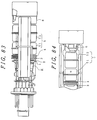
- Fig. 83 is a side elevation showing the entirety of an electron gun of the type for applying a focusing voltage to electrodes G3 and G5 and an anode voltage only to an electrode G6 in accordance with an electron gun for a cathode ray tube
- Fig. 84 is a partial section showing an essential portion of the same.
- the electron gun is equipped, as viewed from the side of a cathode K, with a first electrode 1 (G1), a second electrode 2 (G2), a third electrode 3 (G3), a fourth electrode 4 (G4), a fifth electrode 5 (G5) and a sixth electrode 6 (G6).
- the fifth electrode 5 (G5) is composed of two electrodes 51 and 52.
- the electron beam transmitting hole of the first electrode 1 close to the cathode K is shaped to exert influences upon the spot shape of the electron beam in a low current range
- the electron beam transmitting hole of the second electrode 2 is shaped to exert influences upon the spot shape of the electron beam from a low current range to a high current range.
- the electron beam transmitting holes of the fifth electrode 5 and the sixth electrode forming the main lens are shaped to exert high influences upon the electron beam spot shape in a high current range but lower influences upon the electron beam spot shape in a low current range than in the aforementioned high current range.
- the length of the fourth electrode 4 of the aforementioned electron gun in the axial direction exerts influences upon the magnitude of the optimum focusing voltage and serious influences upon the difference between the individual optimum focusing voltages for low and high currents, respectively, but the length of the fifth electrode 5 in the axial direction exerts far lower influences than those of the fourth electrode 4.
- the shadow mask pitch in a direction perpendicular to the electron beam scanning direction of the cathode ray tube is reduced or the density of the electron beam scanning lines is increased so as to increase the resolution in the direction perpendicular to the electron beam scanning direction, an optical interference occurs especially in a low current range of the electron beam between the electron beam and the shadow mask.
- the prior art has failed to solve the aforementioned various problems.
- An object of the present invention is to solve the problems of the prior art described above and to provide both a cathode ray tube equipped with an electron gun having a construction capable of improving the focusing characteristics over the entire region of the screen and overthe entire current range of an electron beam without supplying any dynamic focusing voltage, to achieve a satisfactory resolution and to reduce the Moire in a low current range, and a deflection aberration correcting method of the same.
- Figs. 85A and 85B presenting a schematic sections showing an essential portion for comparing the structures of the electron gun in dependence upon how to apply a focusing voltage
- Fig. 85A shows a fixed focusing voltage system
- Fig. 85B shows a dynamic focusing voltage system.
- the electrode construction of the fixed focusing voltage type electron gun of Fig. 85 A is identical to that shown in Figs. 83 and 84, and the portions having the same operations are designated at the same reference numerals.
- the electrodes 51 and 52 constituting the fifth electrode 5 are fed with a focusing voltage V *1 at the common potential.
- the two electrodes 51 and 52 constituting the fifth electrode 5 (G5) are fed with different focusing potentials.
- one electrode 52 is fed with a dynamic focusing electrode dV f .
- this dynamic focusing voltage type electron gun has its portion penetrating into another electrode, as indicated at 43, and has a more complicated structure than that of the electron gun shown in Fig. 85A.
- the dynamic focusing voltage type election gun has disadvantages of a higher cost of the parts and a complicated assembly of an electron gun.
- Figs. 86A and 86B are explanatory diagrams plotting the focusing potentials to be supplied to the electron gun shown in Figs. 85A and 85B.
- Fig. 86A is a diagram illustrating the focusing voltage waveform of the focusing voltage type electron gun
- Fig. 86B is a diagram illustrating the waveform of the focusing voltage waveform of the dynamic focusing voltage type electron gun.
- Fig. 86B shows a fixed focusing voltage V f1 , and a voltage comprising another fixed focusing voltage V f20 and a dynamic focusing voltage V f2 superposed upon V f20 .
- the dynamic focusing voltage type electron gun shown in Fig. 85B is required to have two dynamic focusing voltage feeding pins at the stem of the cathode ray tube, and more care than that of the fixed focusing voltage type electron gun of Fig. 86A are required for the insulation from other stem pins.
- Another object of the present invention is to solve the aforementioned problems of the prior art and to provide both a cathode ray tube equipped with an electron gun having a construction capable of improving the focusing characteristics over the entire region of the screen and over the entire current range of an electron beam with the low dynamic focusing voltage to achieve a satisfactory resolution, and a deflection aberration correcting method of the same.
- Still another object of the present invention is to provide both a cathode ray tube for reducing a deterioration in the focusing characteristics due to the space charge repulsion of an electron beam acting between the fluorescent face of the cathode ray tube and the main focusing lens of an electron gun, and a deflection aberration correcting method of the same.
- the distance between the fluorescent face and the main focusing lens of the electron gun becomes the larger for the larger size of the fluorescent face thereby to increase the deterioration in the focusing characteristics due to the space charge repulsion of the electron beam acting in that region.
- a further object of the present invention is to provide an electron gun capable of improving the aforementioned focusing characteristics and shortening the total length of a cathode ray tube, a cathode ray tube equipped with that electron gun, and a deflection aberration correcting method of the cathode ray tube.
- a further object of the present invention is to provide an electron gun free from any deterioration in uniformity of an image over the entire screen even if a cathode ray tube has its deflection angle widened, a cathode ray tube equipped with that electron gun, and a deflection aberration correcting method of the cathode ray tube.
- the total length of the cathode ray tube can be shortened.
- the existing TV set has its depthwise size determined by the total length of the cathode ray tube, and its shorter depth is the more desirable if it is thought as a kind of furniture. Moreover, the shorter depth of the TV set is the more preferable for transportation efficiency in case a large number of TV sets are to be transported from their maker.
- the present invention has structures, as defined in the appended Claims.
- a cathode ray tube comprising an electron gun having a plurality of electrodes, a deflector and a fluorescent face, wherein the improvement resides in that a deflection aberration is corrected by forming a fixed inhomogeneous electric field in the deflecting magnetic field.
- the correction of the deflection aberration is characterized by correcting the deflection aberration in accordance with the deflection by establishing a fixed inhomogeneous electric field having an astigmatism in the deflecting magnetic field.
- the aforementioned fixed inhomogeneous electric field is characterized by establishing an astigmatic inhomogeneous electric field, in which the electron beam is diverged or converged,and correcting the deflection aberration in accordance with the deflection in the scanning line direction of the electron beam or in a direction perpendicular to the scanning line.
- the present invention is characterized in that the deflection aberration is corrected according to the deflection by establishing a fixed inhomogeneous electric field having a coma aberration in a deflecting magnetic field.
- the aforementioned fixed inhomogeneous electric field is characterized by establishing an inhomogeneous electric field having a coma aberration for diverging or converging the electron beam and by correcting the deflection aberration in accordance with the deflection in the scanning line direction of the electron beam or in a direction perpendicular to the scanning line.
- the portions of the fixed inhomogeneous electric field establishing electrode as correspond to the side ones of the three electron beams, can be given different structures between the side of the center electron beam in the in-line direction and in the opposite side to reduce the coma aberration due to the deflecting magnetic field.
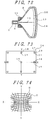
- Fig. 72 is a schematic diagram for explaining the section of a shadow mask type color cathode ray tube equipped with the in-line electron gun.
- reference numeral 7 designates a neck; numeral 8 a funnel; numeral 9 an electron gun mounted in the neck 7; numeral 10 an electron beam; numeral 11 a deflection yoke; numeral 12 a shadow mask; numeral 13 a fluorescent film forming the fluorescent face; and numeral 14 a panel (or screen).
- the electron beam 10 emitted from the electron gun 9 is guided to pass through the shadow mask 12 while being deflected horizontally and vertically by the deflection yoke 11, to fluoresce the fluorescent film 13.
- This fluorescing pattern is observed as an image from the side of the panel 14.
- Fig. 73 is an explanatory diagram showing an electron beam spot in case the periphery of a screen is caused to fluoresce with an electron beam spot having a circular shape at the central portion of the screen.
- the reference numeral 14 designates the screen; numeral 15 a beam spot at the central portion of the screen; numeral 16 beam spots at the ends of the horizontal direction (i.e., X - X direction) of the screen; numeral 17 a halo; numeral 18 beam spots at the ends of the vertical direction (i.e., Y - Y direction) of the screen; and numeral 19 beam spots at the ends of the diagonal directions (i.e., corner portions) of the screen.
- Fig. 74 is an explanatory diagram showing a distribution of the deflecting magnetic field of a cathode ray tube.
- Letter H indicates the distribution of the horizontally deflecting magnetic field
- letter V indicates the distribution of the vertically deflecting magnetic field.
- the color cathode ray tube of recent years uses the pin cushion type non-uniform magnetic field distribution as the horizontally deflecting magnetic field H and the barrel type non-uniform magnetic field distribution as the vertically deflecting magnetic field V, as shown in Fig. 74.
- the shape of the eight emitting spot by the electron beam 10 is not circular in the peripheral portion of the screen partly because of that magnetic field distribution, partly because the electron beam 10 has different orbits at the central portion and in the periphery of the fluorescent face (or the screen), and partly because the electron beam 10 impinges upon the peripheral portion of the screen obliquely with respect to the fluorescent film 13.
- the beam spots 16 at the horizontal ends are horizontally elongated and have the haloes 17, although the central spot 15 is circular.
- the beam spots 16 at the horizontal ends are enlarged and are made ambiguous at their contours by the haloes 17 so that the resolution is deteriorated to degrade the picture quality seriously.
- the electron beam 10 has a low current, its vertical diameter excessively reduced to cause an optical interference with the vertical pitch of the shadow mask 12 so that the Moire phenomena are exhibited to degrade the picture quality.
- the spots 18 at the vertical ends of the screen are attended by the haloes 17 to degrade the picture quality as the electron beam 10 is converged upward and downward (i.e., in the vertical directions) to have a vertically shrunk shape by the vertically deflecting magnetic field.
- the electron beam spots 19 at the corner portions of the screen are horizontally elongated like the aforementioned spots 16 and vertically shrunk like the aforementioned spots 18.
- the electron beam 10 is rotated to establish the haloes 17 and to increase the diameter of the light emitting spots themselves so that the picture quality is seriously degraded.
- Fig. 75 is a schematic diagram showing an electronic optical system of the electron gun for explaining a deformation of the electron beam spot.
- the aforementioned system is replaced by an optical system so as to facilitate the understanding.
- Fig. 75 the upper half presents a section of the screen, as taken in the vertical (Y - Y) direction, and the lower half presents a section of the screen, as taken in the horizontal (X - X) direction.
- Reference numerals 20 and 21 designate prep-focus lenses; numeral 22 a pre-stage main lens; and numeral 23 a main lens. These lenses constitute the electronic optical system corresponding to the electron gun of Fig. 72.
- numeral 24 designates a lens established by the vertically deflecting magnetic field
- numeral 25 designates an equivalent lens which includes a lens established by the horizontally deflecting magnetic field and a lens for apparently extending the electron beam in the horizontal directions by the deflections as a result that the electron beam obliquely impinges upon the fluorescent film 13.
- an electron beam 27 emitted from a cathode K and appearing in the vertical section of the screen establishes a crossover P at a distance l 2 from the cathode K between the pre-focus lenses 20 and 21 and is then converged toward the fluorescent film 13 by the pre-stage main lens 22 and the main lens 23.
- the electron beam passes through an orbit 28 at the central portion of the screen, in which the deflection is zero, and impinges upon the fluorescent film 13.
- the electron beam is vertically shrunk through an orbit 29 by the action of the lens 24 caused by the vertically deflecting magnetic field to form a vertically shrunk beam spot.
- part of the electron beam is focused, as indicated by an orbit 30, before it reaches the fluorescent film 13. This premature focusing forms the haloes 17 of the beam spot 18 at the vertical ends of the screen and the haloes 17 of the beam spots 19 at the corner portions, as shown in Fig. 73.
- an electron beam 31 emitted from the cathode K and appearing in the horizontal section of the screen is converged like the aforementioned electron beam 27 in the vertical section by the pre-focus lenses 20 and 21, the pre-stage main lens 22 and the main lens 23 so that it passes through an orbit 32 at the central portion of the screen, in which the deflecting magnetic field has a zero action, and impinges upon the fluorescent film 13.
- the electron beam is diverged into a horizontally elongated spot shape along an orbit 33 by the diverging action of the lens 25 established by the horizontally deflecting magnetic field but without any halo in the horizontal directions.
- the spot of the electron beam of the electron beam is shaped circular at the central portion of the screen in the rotationally symmetric lens system which is constructed to make the lens system of the electron gun common to the horizontal direction and the vertical direction, the spot shape of the electron beam is distorted in the peripheral portion of the screen to degrade the picture quality seriously.
- Fig. 76 is an explanatory diagram showing means for suppressing degradation in the picture quality In the peripheral portion of the screen, as described in Fig. 75.
- the same reference numerals as those of Fig. 75 designate the same portions.
- the converging action of a main lens 23-1 in the vertical (Y - Y) section of the screen is made weaker than that of the main lens 23 in the horizontal (X - X) section.
- the orbit of the electron beam becomes an orbit as indicated at 29 even after having passed through the lens 24 established by the vertical deflecting magnetic field so that such an extreme vertical shrinkage as has been described with reference to Fig. 73 does not occur and haloes do not occur so easily.
- the orbit 28 at the central portion of the screen is shifted in the direction to increase the spot diameter of the electron beam.
- Fig. 77 is a schematic diagram for explaining the electron beam spot shape on the fluorescent face 14 in case the lens system shown in Fig. 76 is used.
- the haloes are suppressed at the beam spots 16 of the horizontal ends, the beam spots 18 of the vertical ends and the beam spots 19 of the corner portions, i.e., the beam spots of the peripheral portions of the screen so that the resolutions at those portions are improved.
- the vertical spot diameter dY is larger than the horizontal spot diameter dX so that the vertical resolution drops.
- the object of improving the resolutions of the entire screen at the same time is not basically solved by making the rotationally asymmetric electric field system in which the converging effects of the main lens 23 are different between the vertical direction and the horizontal direction of the screen.
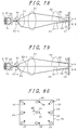
- Fig. 78 is a schematic diagram showing an electronic optical system of the electron gun which has not the lens intensity of its main lens 23 made rotationally asymmetric but the lens intensity of its pre-focus lens 21 increased in a horizontal direction (X - X).
- the electron beam spot diameter of the fluorescent film 13, as taken in the horizontal direction, can be reduced by making the intensity of a horizontal pre-focus lens 21-1 for diverging the image of the crossover point P higher than that of the vertical pre-focus lens to increase the angle of incidence of the electron beam 31 into the pre-stage main lens 22 thereby to enlarge the diameter of the electron beam to pass through the main lens 23.
- the electron beam orbit in a vertical direction of the screen is similar to that shown in Fig. 75 so that it has no effect for suppressing the halo 28.
- Fig. 79 is a schematic diagram showing the electronic optical system of an electron gun in which a halo suppressing effect is added to the construction of Fig. 77.
- the pre-stage main lens is given an increased lens intensity in the vertical (Y - Y), as indicated at 22-1, the vertical electron beam orbit of the main lens 23 comes close to the optical axis to form a focusing system having an increased focal depth so that the halo 28 becomes inconspicuous to improve the resolution.
- Fig. 80 is a schematic diagram for explaining the spot shape of the electron beam on the screen 14 when the lens system having the construction shown in Fig. 79 is used. It is seen that an excellent resolution having no halo all over the screen is achieved, as indicated by the beam spots 15, 16, 18 and 19.
- the description thus far made is directed to the electron beam spot shapes in case the electron beam has a relatively high current (i.e., in a high current range).
- the orbit of the electron beam passes only near the axis of the focusing system so that the difference between the horizontal and vertical lens intensities of the lenses 21, 22 and 23 having large apertures exerts little influence.
- the beam spots are circular (at 34) at the central portion of the screen, horizontally elongated (at 35, 36) or obliquely elongated (at 37) in the peripheral portions of the screen to cause the Moire phenomena.
- the resolution drops as the transverse (or horizontal) diameters of the beam spots increase.
- Fig. 81 is a schematic diagram showing the electron gun optical system for explaining the orbit of an electron beam for a low current.
- the distance l 2 from the cathode K to the crossover point P is shorter than the distance l 1 in Fig. 75.
- Fig. 82 is a schematic diagram showing the optical system of the electron gun in case the lens intensity of a diverging lens in the pre-focus lens is increased in the vertical (Y - Y) direction of the screen.
- the distance l 3 to the crossover point P from the cathode K is made longer than the aforementioned distance l 2 by increasing the vertical intensity of the diverging lens composing the pre-focus lens 20.
- the position for the electron beam 27 to enter the pre-focus lens 21, as taken in the vertical section comes closer to the axis than that in the case of Fig. 81 so that the lens effects of the lenses 21, 22-1 and 23 are weakened to provide a focusing system having a larger focal depth in the direction vertical of the screen.
- the structures of the main lenses to be adopted and the picture qualities to be improved differ with applications of the cathode ray tube. Therefore, the positions of the rotationally asymmetric lenses and the intensities of the individual lenses are not uniquely determined.
- a lens for establishing the rotationally asymmetric electric field in different portions for the high current range and for the low current range has to be provided for improving the resolution for the entire current range.
- the rotationally asymmetry of each lens is limited in the change of the electric field intensity. In dependence upon the lens portion, moreover, the beam shape is extremely distorted to cause the drop of the resolution if the intensity of the rotationally asymmetric electric field is increased.
- the means thus far described is a general one for suppressing the drop of the focusing characteristics due to the deformation of the spot of the electron beam.
- the actual electron gun is exemplified by one using the fixed focusing voltage as described hereinbefore, and one using the optical focusing voltage varying dynamically in accordance with the deflection angle on the screen of the cathode ray tube.
- the electron gun using the fixed focusing voltage has a low cost and a simple power source circuit for feeding the focusing voltage so that its circuit cost is reasonable.
- the optimum focused states cannot be achieved at the individual positions on the screen of the cathode ray tube because of the astigmatic correction.
- the beam spots have larger diameters than optimum beam spots individually focused at individual points.
- the electron gun using the optimum focusing voltage varying dynamically in accordance with the deflection angle on the screen of the cathode ray tube can achieve excellent focusing characteristics at the individual points on the screen.
- the structure of the electron gun and the power source circuit for feeding the focusing voltage are complicated, and it takes a long time to set the focusing voltage on the assembly line of the TV set or the display terminal, so that the production cost is raised.
- the present invention contemplates to provide a crt using an electron gun which has the individual merits of the above-specified two structures while eliminating the demerits and which also has such a third merit of a small axial length as could not be achieved by the two structures.
- the cathode ray tube has its deflection aberration augmented abruptly as the deflection increases, as has been described with reference to Fig. 66.
- the present invention contemplates to make a proper electron beam converging action possible to improve the homogeneity of resolution on a fluorescent face by establishing such an inhomogeneous electric field positioned in a deflecting magnetic field as will change the converging or diverging action of the electron beam when the electron beam is deflected to have its orbit changed.
- the present invention also contemplates to correct the deflection aberration, which will be abruptly augmented according to the deflection, as shown in Fig. 66, to make the proper electron beam converging action possible all over the fluorescent face by forming such an inhomogeneous electric field positioned in the deflecting magnetic field as will has its deflection aberration correction accelerated according to the deflection, as has been described with reference to Fig. 67, when the electron beam is deflected to have its orbit changed. This makes it possible to improve the homogeneity of the resolution all over the fluorescent face.
- An electric field having an astigmatism is effective as one of the inhomogeneous electric fields which are positioned in the deflecting magnetic field for accelerating the converging or diverging action of the electron beam properly according to the deflection when the deflected electron beam has its orbit changed.
- the electric field having the astigmatism is formed of an electric field having two orthogonal planes of symmetry.
- the converging or diverging action is increased the more for the larger distance from the center to the end of the plane of symmetry.
- Fig. 1 is a schematic diagram showing a first embodiment of the deflection aberration correcting method of a cathode ray tube according to the present invention and shows an example of the distribution of the astigmatic electric field, in which the electron beam has the diverging action, on one plane of symmetry.
- Fig. 1 reference numeral 61 designates equipotential lines; numeral 62 designates an electron beam passing through the center of the electric field; and numeral 63 designates electron beam passing through portions apart from the center of the electric field.
- Fig. 1 illustrates the comparison between the statuses of the electron beam 62 passing through the center of the electric field established by the equipotential lines 61 and the electron beam 63 passing through the portion apart from the center of the electric field.
- the electron beam 63 passing apart from the center of the electric field has the larger divergence to approach the end of the electric field in its entirety than the electron beam 62 passing through the center of the electric field as it flies the more in the electric field. Moreover, the change of the orbit is the greater at the closer position to the end of the electric field.
- the interval of the equipotential lines 61 becomes the narrower from the longer distance from the axis of symmetry Z - Z of the electric field.
- the distance from the main lens of the electron lens to the fluorescent face is generally longer in the periphery of the fluorescent face than at the center of the fluorescent face, as shown in Fig. 68, an over-convergence occurs in the periphery of the fluorescent face if the electron beam is optimized in the convergence at the center of the fluorescent face even in case that no converging action is exerted on the electron beam of the deflecting magnetic field.
- the diverging action is increased with the increase in the deflection by establishing the fixed electric field, as shown in Fig. 1, in the deflecting magnetic field, so that the deflection aberration correction can be accomplished, as shown in Fig. 67.
- Fig. 2 is a schematic diagram showing a second embodiment of the deflection aberration correcting method of a cathode ray tube according to the present invention, and shows an example of the astigmatic electric field, in which the electron beam has the converging action, on one plane of symmetry.
- Fig. 2 there are compared the statuses of the electron beam 62 passing through the center of the electric field established by the equipotential lines 61 and the electron beam 63 passing through the portion apart from the center of the electric field.
- the electron beam 63 passing apart from the center of the electric field acquires a larger convergence than that of the electron beam 62 passing through the center of the electric field, as it progresses in the electric field, and has its entire orbit brought toward the center of the electric field. Moreover, the changing force of the orbit is the larger at the closer side to the end of the electric field. This is because the interval of the equipotential lines 61 becomes the narrower as it leaves the axis of symmetry Z - Z of the electric field the more.
- the electron beam is deflected to have its orbit changed. Then, the converging action of the electron beam can be accelerated according to the deflection to correct the deflection aberration correction of the case in which the deflection aberration enhances the divergence of the electron beam.
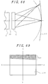
- the deflection of the cathode ray tube is frequently effected by the method of scanning the electron beam linearly, as shown in Fig. 69.
- This linear scanning locus 60 is called the "scanning line.”
- the deflecting magnetic field is frequently different in the direction of the scanning line and in the perpendicular direction.
- the electron beam is frequently different in the converging action between the direction of the scanning line and the perpendicular direction by the action of at least one of the aforementioned plurality of electron gun electrodes before it heavily receives the action of the fixed inhomogeneous electric field to be formed in the deflecting magnetic field.
- the weighing is different depending upon the application of the cathode ray tube between the correction of deflection aberration in the direction of the scanning line and the correction of the deflection aberration in the direction perpendicular to the scanning line.
- the constitution of the fixed astigmatic electric field to be formed in the deflecting magnetic field is not uniquely determined. It is important for improving the characteristics of an image display device and for realizing a low price to clarify and copy with the characteristics to be corrected according to the individual situations in which the corresponding technical solution and the necessary cost are not always identical depending upon the direction of correction with respect to the direction of the scanning line and the method and amount of correction.
- a third embodiment of the deflection aberration correcting method of the cathode ray tube according to the present invention is to establish the inhomogeneous electric field, as shown in Figs. 1 and 2, in the deflecting magnetic field to effect the deflection aberration in the scanning line direction and in the perpendicular direction to the sanning line.
- the vertical deflecting magnetic field is exemplified by a barrel-shaped magnetic field distribution whereas the horizontal deflecting magnetic field is exemplified by a pin-cushion shaped magnetic field distribution, as shown in Fig. 74, so as to simplify the circuit for controlling the convergencies of the three electron beams at a point on the fluorescent face.
- the two side electron beams receive the different amounts of deflection aberration from the vertical deflecting magnetic field in dependence upon the magnitude of the vertical deflecting magnetic field and the direction with respect to the horizontal deflection. For example, assume that an electron beam is emitted from the righthand side gun of the in-line type gun when the cathode ray tube is viewed from its fluorescent face side.
- a magnetic field distribution of the deflecting magnetic field passed by the electron beam deflected leftward on the fluorescent face with respect to the cathode ray tube axis is different from that passed by the electron beam deflected rightward on the fluorescent face with respect to the cathode ray tube axis, and the amounts of deflection aberration the two beams received are different from each other.
- the image qualities produced by one side gun differ between the righthand and lefthand corners on the fluorescent face.
- it is effective to form the coma aberration fixed electric field in the deflecting magnetic field.
- the electric field having the coma aberration has only one plane of symmetry.
- Fig. 3 is a schematic diagram showing a fourth embodiment of the deflection aberration correcting method of a cathode ray tube according to the present invention, and shoes an example of the coma aberration electric field having the electron beam diverging action on the plane of symmetry.
- the statuses are compared between the electron beam 62 passing through the center of the electric field established by the equipotential lines 61 and an electron beam 63-2 passing through the portion apart from the center of the electric field.
- This comparison reveals that the electron beam 63-2 passing apart from the center of the electric field takes a larger divergence, as it progresses in the electric field, than the electron beam 62 passing through the center of the electric field and has its entire orbit brought closer to the end of the electric field.
- the change of the orbit is the greater at the side close to the end of the electric field. This is because the interval of the equipotential lines 61 becomes the narrower for the longer distance from the axis of symmetry Z - Z.
- An electron beam 63-3 passing through a portion apart from the center of the electric field also has a larger divergence like the electron beam 63-2, as it progresses in the electric field, then the electron beam 62 and has its entire orbit brought closer to the end of the electric field. Moreover, the change of the orbit is also the grater at the side close to the end of the electric field, but the changing rate is lower than that of the electron beam 63-2.
- the deflection aberration correction to be made is one of the case of the converging action in which the deflection aberrations are different depending upon the directions of deflection.
- the deflection aberration correction is not uniquely determined because it depends upon the structure of the cathode ray tube including the maximum deflection angle, the structure of a deflecting magnetic field generating unit to be combined, the electrode for establishing the inhomogeneous electric field, the electron gun structure except the inhomogeneous electric field establishing electrode, the driving conditions of the cathode ray tube, the application of the cathode ray tube and so on.
- Fig. 4 is a schematic diagram showing a fifth embodiment of the deflection aberration correcting method of a cathode ray tube according to the present invention and shows an example of the coma aberration electric field having the electron beam converging action on the plane of symmetry.
- the electron beam 63-4 receives more convergence than the electron beam 62, as it progresses in the electric field, and has its entire orbit brought close to the center of the electric field. Moreover, the change of the orbit is greater at the side closer to the end of the electric field. This is because the interval of the equipotential lines 61 becomes the narrower at the larger distance from the axis of symmetry Z - Z of the electric field.
- the electron beam 63-5 passing through the portion apart from the center of the electric field also receives more convergence like the electron beam 63-4, as its progresses in the electric field, than the electron beam 62 and has its entire orbit brought closer to the center of the end of the electric field.
- the change of the orbit is the higher at the closer side to the end of the electric field, but the changing rate is lower than that of the electron beam 63-4. This is because the interval of the equipotential lines 61 does not become so small even apart from the axis of symmetry Z - Z of the electric field.
- the deflection aberration correction is made for the diverging action in which the deflection aberrations are different depending upon the directions of deflection.
- the deflection aberration correction is not uniquely determined because it depends upon the structure of the cathode ray tube including the maximum deflection angle, the structure of a deflecting magnetic field generating unit to be combined, the electrode for establishing the inhomogeneous electric field, the electron gun structure except the inhomogeneous electric field establishing electrode, the driving conditions of the cathode ray tube, the application of the cathode ray tube and so on.
- the vertical deflecting magnetic field is exemplified by a barrel-shaped magnetic field distribution whereas the horizontal deflecting magnetic field is exemplified by a pin-cushion shaped magnetic field distribution, as shown in Fig. 74, so as to simplify the circuit for controlling the convergence of the three electron beams at a point on the fluorescent face.
- the direction of the in-line array i.e., the aforementioned horizontal direction is the scanning line direction.
- the two side electron beams receive the different amounts of deflection aberration from the vertical deflecting magnetic field in dependence upon the magnitude of the vertical deflecting magnetic field and the direction of the horizontal deflection with respect to the tube axis. For example, assume that an electron beam es emitted from the righthand side gun of the in-line type gun when the cathode ray tube is viewed from its fluorescent face side.
- a magnetic field distribution of the deflecting magnetic field passed by the electron beam deflected leftward on the fluorescent face with respect to the cathode ray tube axis is different from that passed by the electron beam deflected rightward on the fluorescent face with respect to the cathode ray tube axis, and the amounts of deflection aberration the two beams receive are different from each other.
- the coma aberration electric field as shown in Fig. 3 or 4 is formed, as the inhomogeneous fixed electric field in the aforementioned scanning line direction in the deflecting magnetic field corresponding to the two side ones of the in-line arrayed three electron beams, to correct the deflection aberration.
- the deflection aberration correction is not uniquely determined because it depends upon the structure of the cathode ray tube including the maximum deflection angle, the structure of a deflecting magnetic field generating unit to be combined, the electrode for establishing the inhomogeneous electric field, the electron gun structure except the inhomogeneous electric field establishing electrode, the driving conditions of the cathode ray tube, the application of the cathode ray tube and so on.
- Fig. 5 is a schematic section for explaining a first embodiment of the cathode ray tube according to the present invention.
- Reference numeral 1 designates a first electrode (G1) of the electron gun;
- numeral 2 designates a second electrode (G2); and
- numeral 3 designates a third electrode (G3) or a focusing electrode in this embodiment.
- Numeral 4 designates a fourth electrode (G4) or an anode in this embodiment.
- Numeral 7 designates a neck portion of the cathode ray tube for accommodating the electron gun;
- numeral 8 designates a funnel portion; and
- numeral 14 designates a panel portion.
- reference numeral 10 designates an electron beam emitted from the electron gun. This electron beam 10 passes through an aperture of a shadow mask 12 and impinges upon a fluorescent film 13 formed on the inner face of the panel 14 to cause the fluorescent film 13 to fluoresce thereby to make a display on the screen of the cathode ray tube.
- Numeral 11 designates a deflection yoke for deflecting the electron beam 10. This deflection yoke 11 establishes a magnetic field in synchronism with a video signal for controlling the electron beam and controls the position of impingement of the electron beam 10 upon the fluorescent film 13.
- reference numeral 38 designates a main lens of the electron gun.
- the electron beam 10 emitted from a cathode K is focused, after it has passed through the first electrode (G1) 1, the second electrode (G2) 2 and the third electrode (G3) 3, upon the fluorescent face 13 by the electric field of the main lens 38.
- reference numeral 39 designates an electrode which is positioned in the magnetic field of the deflection yoke 11 for establishing an inhomogeneous electric field to correct the deflection aberration of the electron beam 10, when this electron beam 10 is to be deflected by the magnetic field of the deflection yoke 11, in accordance with the deflection angle.
- the deflection aberration correcting electrode 39 is electrically connected with and mechanically fixed on the anode 4 and is composed of two portions in total, i.e., upper and lower ones, as taken in the vertical direction of the electron beam 10, to establish the inhomogeneous electric field acting to diverge the electron beam 10.
- numeral 40 designates leads for connecting the electrodes of the electron gun with the (not-shown) stem pins.
- the gap between the two components of the deflection aberration correcting electrode 39 is made slightly larger on the side of the fluorescent film 13 than on the side of the anode 4.
- the degree of spread of the gap is not uniquely determined because it is determined by the combination of the mounted positions of the two components, the extending length toward the fluorescent film 13, the distribution of the deflecting magnetic field, the diameter of the electron beam passing between the two components, the maximum deflection angle of the cathode ray tube and so on.
- the main lens 38 of the electron gun is shown, as located in a position closer to the fluorescent film 13 than the mounted position of the deflection yoke 11 within the deflecting magnetic field of the yoke 11, but the position of the main lens 38 should not be limited to the shown one if it is within the magnetic field region of the deflection yoke.
- Fig. 6 is a schematic section showing an essential portion for explaining the operations of the cathode ray tube according to the present invention.
- Fig. 6 explains in detail one example of the action of the deflection aberration correcting electrode 39 which is positioned in the magnetic field of the deflection yoke 11 of Fig. 5 for establishing an inhomogeneous electric field to correct the deflection aberration of the electron beam 10, when this beam 10 is to be deflected by the magnetic field of the deflection yoke 11, in accordance with the deflection angle.
- the inhomogeneous electric field acts to diverge the electron beam 10.
- the numeral 38 designates the main lens
- numeral 41 designates a partial electrode forming part of the fourth electrode (G4) 4
- characters L 1 indicate the distance between the main lens 38 and the center of deflection.
- Fig. 7 is a schematic section showing an essential portion similar to Fig. 6 but with a deflection aberration correcting electrode 39 being omitted, for explaining the operations of the deflection aberration correcting electrode 39 or an inhomogeneous electric field establishing electrode in the cathode ray tube according to the embodiment of the present invention, in comparison with the prior art.
- the electron beam 10 having passed through the third electrode (G3) 3 is converged by the main lens 38, which is formed between the third electrode (G3) 3 and the fourth electrode (G4) 4, and is allowed to proceed straight as it is, if it is not deflected (at the central portion of the screen) by the deflecting magnetic field established by the deflection yoke 11, until it is focused into a beam spot having a diameter of D 1 on the fluorescent film 13.
- the lower one of the outer circumferential orbits of the electron beam 10 is not affected by the presence or absence of the deflection aberration correcting electrode 39 but proceeds, as indicated by 10 D .
- the upper outer circumferential orbit proceeds, as indicated by 10 U , because of no action of the deflection aberration correcting electrode 39, and crosses the lower outer circumferential orbit 10 D before it reaches the fluorescent film 13.
- a spot having a diameter D 2 is formed on the fluorescent film 13.
- the orbit portion of the electron beam, as located at the upper side proceeds, as indicated by 10 U ', under the attracting force of the deflection aberration correcting electrode 39.
- the orbit portion of the electron beam, as located at the lower side proceeds, as indicated by 10 D in Fig. 7, because of little influence of the deflection aberration correcting electrode 39, and reaches the fluorescent film 13 without crossing the upper outer circumferential orbit 10 U ' before the arrival.
- a spot having a smaller diameter D 3 than the aforementioned one D 2 is formed on the fluorescent film 13. This is because the aforementioned inhomogeneous electric field is formed, as shown in Fig. 71.
- the distribution of the beam spot of the diameter D 3 on the individual positions of the fluorescent film 13 can be optimzed by combining the mounting positions of the two components of the deflection aberration correcting electrode 39,their extensions toward the fluorescent film 13, the distribution of the deflecting magnetic field, the diameter of the electron beam passing between the two components, the maximum deflection angle of the cathode ray tube and so on, so that a uniform resolution can be achieved all over the screen by reducing the difference from the beam spot diameter D 1 at the central portion of the screen.
- the focused status can be controlled in synchronism with the deflection angle on the fluorescent film (or screen) without supplying any potential dynamically to any of the electrodes of the electron gun in synchronism with the deflection angle of the electron beam, thus, it is possible to provide the cathode ray tube, which has a homogeneous display quality all over the screen at a reasonable cost.
- these conditions are not uniquely determined because they depend upon the structure of the cathode ray tube including the maximum deflection angle, the structure of a deflecting magnetic field generating unit to be combined, the electrode for establishing the inhomogeneous electric field, the electron gun structure except the inhomogeneous electric field establishing electrode, the driving conditions of the cathode ray tube, the application of the cathode ray tube and so on.
- the electron beam has to be so deflected that its orbit may pass through regions having electric field intensities differing with deflection angles.
- the aforementioned inhomogeneous electric field is restricted by the positional relation to the deflecting magnetic field.
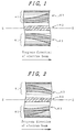
- Fig. 8 is an explanatory diagram plotting an example of the distribution of a deflecting magnetic field, as taken on the axis, for a cathode ray tube having a deflection angle of 100 degrees or more.
- FIG. 9 is an explanatory diagram corresponding to Fig. 8 and shows the positional relations of a deflecting magnetic field establishing mechanism.
- Letter A indicates a reference position for measuring the metering time of the magnetic field
- letters BH indicate a position having the maximum magnetic flux density of the magnetic field distribution 64 for deflecting in the scanning line direction
- letters BV indicate a position having the maximum magnetic flux density of the magnetic field distribution 65 for deflecting in the direction perpendicular to the scanning line
- letter C indicates an end portion of the magnetic material for making up the core of a coil for establishing the deflecting magnetic field, on the side remote from the fluorescent face of the cathode ray tube.
- the aforementioned distance takes the maximum in case the electrodes on the side of the fluorescent face are complicated in the axial direction of the cathode ray tube.
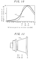
- Fig. 10 is an explanatory diagram plotting an example of the distribution of a deflecting magnetic field, on the axis for a cathode ray tube having a deflection angle of 100 degrees or less.
- FIG. 10 is an explanatory diagram corresponding to Fig. 10 and shows the positional relations of a deflecting magnetic field establishing mechanism.
- Letter A indicates a reference position for measuring the magnetic field
- letters BH indicates a position having the maximum magnetic flux density of the magnetic field distribution 64 for deflecting in the scanning line direction
- letters BV indicate a position having the maximum magnetic flux density of the magnetic field distribution 65 for deflecting in the direction perpendicular to the scanning line
- letter C indicates an end portion of the magnetic material for making up the core of a coil for establishing the deflecting magnetic field, on the side remote from the fluorescent face of the cathode ray tube.
- Fig. 12 is a perspective view showing an example of the structure of the deflection aberration correcting electrode for establishing an inhomogeneous fixed electric field in the deflecting magnetic field of the present invention.
- the deflection aberration correcting electrode 39 of Fig. 12 is composed of two folded metal plates which are opposed in parallel to each other with a distance therebetween F.
- the portion D is positioned on the side close to the fluorescent face of the cathode ray tube whereas the portion E is positioned on the side close to the fluorescent face so that the center of the opposed portions may transmit the electron beam therethrough if there is established no deflecting magnetic field.
- the deflection aberration correcting electrode 39 is disposed that the opposed portions G may be in parallel with the scanning line, and is actually welded together with the anode of the cathode ray tube in the color cathode ray tube having a neck external diameter of 29 mm, a maximum deflection angle of 108 degrees and a fluorescent face size of 59 cm.
- a satisfactory result is obtained by combining the deflecting magnetic field of Fig. 8 with the cathode ray tube, by placing the D-side front end in Fig. 12 at a position of 108 mm in the Z-axis of Fig. 8 and by using an anode voltage of 30 KV.
- the magnetic flux density at the position,at which the D-side front end in Fig. 12 is set is 0.0086 millitesla per root of the anode voltage of 1 V. This value is about 33% of the maximum magnetic flux density.
- the distance of the coil for establishing the deflecting magnetic field from the core end portion remote from the fluorescent face is about 30 mm.
- the deflection aberration correcting electrode for establishing an inhomogeneous fixed electric field in the deflection aberration shown in Fig. 12 is used like before in the cathode ray tube and is welded together with the anode of the electron gun in a color cathode ray tube having a neck portion external diameter of 29 mm, a maximum deflection angle of 90 degrees and a fluorescent face size of 48 cm.
- a satisfactory result is obtained by combining the deflecting magnetic field of Fig.10 with the cathode ray tube , by placing the D-side front end in Fig. 12 at a position of 70 mm in the Z-axis of Fig.10 and by using an anode voltage of 30 kV.
- the magnetic flux density at the position, at which the D-side front end in Fig. 12 is set is 0.01 millitesla per root of the anode voltage of 1 V. This value is about 50 % of the maximum magnetic flux density.
- the distance of the coil for establishing the deflecting magnetic field from the core end portion remote from the fluorescent face is about 13 mm.
- Fig. 13 is a section showing an essential portion of one example of an electron gun to be used in the cathode ray tube according to the present invention.
- anode 6 which is located close to the fluorescent face
- a focus electrode 5 which is located remote from the fluorescent face.
- the deflection aberration correcting electrode 39 for establishing a fixed inhomogeneous electric field in the deflecting magnetic field is positioned closer to the fluorescent face than that end 6a of the anode 6 of the electron gun, which is opposed to the main lens 38.
- Fig. 14 is a section showing an essential portion of one example of an electron gun to be used in the cathode ray tube according to the present invention.
- anode 6 which is located close to the fluorescent face
- a focus electrode 5 which is located closer to the cathode K than the anode 6.
- the deflection aberration correcting electrodes for establishing a fixed inhomogeneous electric field in the deflecting magnetic field is disposed at two positions 39 and 39-2.
- the deflection aberration correcting electrode 39-2 is positioned closer to the cathode than that end 6a of the anode 6 of the electron gun, which is opposed to the main lens 38.
- Fig. 15 is a section showing an essential portion of one example of an electron gun to be used in the cathode ray tube according to the present invention.
- the cathode ray tube is exemplified by a projection type cathode ray tube having a maximum deflection angle of 85 degrees or less.
- an electromagnetically focusing coil 74 is disposed outside of the neck portion closer to the fluorescent face 13 than the anode 4. Moreover, a distance L from an end 4a of the anode 4 facing the main lens to the end portion of the deflection aberration correcting electrode 39, as located near the fluorescent face 13, for establishing the fixed inhomogeneous electric field in the deflecting magnetic field is about 180 mm.
- the end 4a of the anode 4 facing the main lens 38 is a cylinder having an aperture diameter of 30 mm.
- the potential of the fluorescent film is divided by a resistive film 75 formed on the inner face of the neck portion and a resistor 76 to generate a voltage to be fed to the anode 4.
- the detailed conditions are not uniquely determined because they depend upon the structure of the cathode ray tube including the maximum deflection angle, the structure of a deflecting magnetic field generating unit to be combined, the electrode for establishing the inhomogeneous electric field, the electron gun structure except the inhomogeneous electric field establishing electrode, the driving conditions of the cathode ray tube, the application of the cathode ray tube and so on.
- the distance from the end 6a of the anode 6 of the electron gun facing the main lens 38 to the cathode is 100 mm.
- the end 6a of the anode 6 facing the main lens 38 is a cylinder having an aperture diameter of 20 mm.
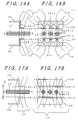
- Figs. 16A and 16B are diagrams showing an essential portion for explaining an example of the structure of a deflection aberration correcting electrode, in which the present invention is applied to a color cathode ray tube using three electron beams arranged in-line.
- Fig. 16A presents a transverse section
- Fig. 16B presents a front elevation.
- reference numeral 77 designates lines of magnetic force for deflecting the electron beam 10 in the in-line array direction.
- the magnetic material 39-1 as a portion of the deflection aberration correcting electrode 39 for establishing a fixed inhomogeneous electric field in the deflecting magnetic field, the lines of magnetic force 77 are concentrated in the vicinity of the electron beam 10 to promote the deflecting action of the corresponding portion.
- Figs. 17A and 17B are diagrams showing an essential portion for explaining another example of the structure of a cathode ray tube of the present invention, in which the deflection aberration correcting electrode is applied to a color cathode ray tube using three electron beams arranged in-line.
- Fig. 17A presents a transverse section
- Fig. 17B presents a front elevation.
- no concentration of the lines of magnetic force occurs because the aforementioned magnetic material 39-1 is not disposed in the deflection aberration correcting electrode 39.
- the direction for promoting the deflection is not uniquely determined because it depends upon the structure of the cathode ray tube including the maximum deflection angle, the structure of a deflecting magnetic field generating unit to be combined, the electrode for establishing the inhomogeneous electric field, the electron gun structure except the inhomogeneous electric field establishing electrode, the driving conditions of the cathode ray tube, the application of the cathode ray tube and so on.
- Figs. 18A and 18B are diagrams showing an essential portion for explaining another example of the structure of a deflection aberration correcting electrode, in which the present invention is applied to a color cathode ray tube using three electron beams arranged in-line.
- Fig. 18A presents a transverse section
- Fig. 18B presents a front elevation.
- the deflection aberration correcting electrode 39 has its aperture 78 shaped to envelope the electron beams 10.
- the color cathode ray tube using the in-line arrayed three electron beams, as shown has its scanning line direction in parallel with the in-line direction so that the aperture 78 of the deflection aberration correcting electrode 39 for establishing the fixed inhomogeneous electric field in the deflecting magnetic field, as shown, corresponds to the scanning line direction.
- the detailed conditions are not uniquely determined because they depend upon the structure of the cathode ray tube including the maximum deflection angle, the structure of a deflecting magnetic field generating unit to be combined, the electrode for establishing the inhomogeneous electric field, the electron gun structure except the inhomogeneous electric field establishing electrode, the driving conditions of the cathode ray tube, the application of the cathode ray tube and so on.
- Figs. 19A and 19B are diagrams similar to Figs. 18A and 18B but show an essential portion for explaining still another example of the structure of a deflection aberration correcting electrode, in which the present invention is applied to a color cathode ray tube using three electron beams arranged in-line.
- Fig. 19A presents a transverse section
- Fig. 19B presents a front elevation.
- the deflection aberration correcting electrode 39 has its aperture 78 shaped to envelope the electron beam 10.
- the color cathode ray tube using the in-line arrayed three electron beams, as shown has its scanning line direction in parallel with the in-line direction so that the aperture 78 of the deflection aberration correcting electrode 39 for establishing the fixed inhomogeneous electric field in the deflecting magnetic field, as shown, corresponds to the scanning line direction.
- the aperture diameter of the aperture 78 is not uniform in the direction perpendicular to the scanning line and has the smallest size F located at the portion facing each electron beam.
- the deflection aberration correction is changed according to the deflection even in case the electron beam is deflected in the in-line direction.
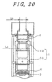
- the size F is set to 3 mm, and the deflection aberration correcting electrode 39 is attached to the electron gun, as shown in Fig. 20.
- a satisfactory result is obtained by setting the aperture diameters, as taken in the scanning line direction and in the perpendicular direction, of the end of the electron gun anode facing the main lens to 8 mm.
- the detailed conditions are not uniquely determined because they depend upon the structure of the cathode ray tube including the maximum deflection angle, the structure of a deflecting magnetic field generating unit to be combined, the electrode for establishing the inhomogeneous electric field, the electron gun structure except the inhomogeneous electric field establishing electrode, the driving conditions of the cathode ray tube, the application of the cathode ray tube and so on.
- the value F may be zero.
- Figs. 16A and 16B only the front end 39-2 of the opposing portion facing the electron beam 10 protrudes toward the direction A. On the contrary, the same portion uniformly protrudes in Figs. 17A and 17B. These protrusions are not dependent upon only the material of the deflection aberration correcting electrode 39 but can occur in the case of a non-magnetic material.
- the scanning line direction of the color cathode ray tube using the in-line arrayed three electron beams is in parallel with the in-line direction so that the opposing portion of the deflection aberration correcting electrode 39 for establishing the fixed inhomogeneous electric field in the deflecting magnetic field in the Figures is in line with the scanning line direction.
- Fig. 20 is an explanatory diagram showing an example of the structure of an electron gun having the deflection aberration correcting electrode mounted thereon.
- the deflection aberration correcting electrode 39 is attached to the electron gun, as shown in Fig. 20, by setting the distance F between the opposing front ends 39-2 in the direction perpendicular to the scanning lines to 3 mm. At this time, a satisfactory result is achieved by setting the aperture diameter, as taken in the direction perpendicular to the scanning line, of the electron gun anode facing the main lens to 8 mm.
- the detailed conditions are not uniquely determined because they depend upon the structure of the cathode ray tube including the maximum deflection angle, the structure of a deflecting magnetic field generating unit to be combined, the electrode for establishing the inhomogeneous electric field, the electron gun structure except the inhomogeneous electric field establishing electrode, the driving conditions of the cathode ray tube, the application of the cathode ray tube and so on.
- Figs. 21A and 21B are explanatory diagrams showing another example of the structure of the deflection aberration correcting electrode in the electron gun used in the cathode ray tube of the present invention.
- the deflection aberration correcting electrode 39 for forming the fixed inhomogeneous electric field in the deflecting magnetic field is connected with the fluorescent face of the cathode ray tube so that it is fed with the same potential as the fluorescent face.
- the potential of the anode 60 of the electron gun is obtained by dividing the potential of the fluorescent face by voltage dividing resistors 69 and 70 within the cathode ray tube. That terminal of the resistor 70 which is not connected with the anode 6 is led to the outside of the cathode ray tube and is directly grounded to the earth or connected with another power source.
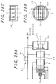
- Figs. 22A-22C are explanatory diagrams showing still another example of the structure of the deflection aberration correcting electrode in the electron gun used in the cathode ray tube of the present invention.
- the power feed of Fig. 77 is grounded through a variable resistor to adjust the anode voltage from the outside of the cathode ray tube.
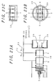
- Figs. 23A-23C are explanatory diagrams showing a further example of the structure of the deflection aberration correcting electrode in the electron gun used in the cathode ray tube of the present invention.
- the deflection aberration correcting electrode 39 for forming the fixed inhomogeneous electric field in the deflecting magnetic field is connected with the fluorescent face of the cathode ray tube and is fed with the same potential as that of the fluorescent face.
- the potential of the anode 6 of the electron gun is obtained by dividing the potential of the fluorescent face by the resistors 69 and 70 within the cathode ray tube and the resistor 70 is connected with the focus electrode 5 within the cathode ray tube and can be adjusted together with the focus voltage when assembled in the image display device.
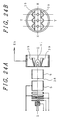
- Figs. 24A and 24B are explanatory diagrams showing a further example of the structure of the deflection aberration correcting electrode in the electron gun used in the cathode ray tube of the present invention.
- the deflection aberration correcting electrode 39 for forming the fixed inhomogeneous electric field in the deflecting magnetic field is fed with the same potential as that of the anode 6 of the electron gun. Thanks to this connection, no special potential supply is necessary including that for the deflection aberration correcting electrode 39, and the considerations to be taken into the voltage withstanding characteristics of the individual electrodes can be minimized to simplify the assembly of the electron gun. Thus, it is possible to provide a cathode ray tube at a reasonable cost.
- Figs. 25A-25C are explanatory diagrams showing a further example of the structure of the deflection aberration correcting electrode in the electron gun used in the cathode ray tube of the present invention.
- the deflection aberration correcting electrode 39 for forming the fixed inhomogeneous electric field in the deflecting magnetic field is fed with the same potential as that of the anode 6 of the electron gun, but the anode 6 is formed with an aperture 71 in addition to the electron beam transmitting hole so that the electric field to be established between the anode 6 and an electrode at a potential different from that of the anode 6 may penetrate through the aperture 71 into the vicinity of the deflection aberration correcting electrode 39 to control the aforementioned inhomogeneous electric field.
- Figs. 26A and 26B are explanatory diagrams showing a further example of the structure of the deflection aberration correcting electrode in the electron gun used in the cathode ray tube of the present invention.
- Fig. 26A presents a schematic diagram showing the construction of the electron gun
- Fig 26B presents a front elevation of the deflection aberration correcting electrode.
- the deflection aberration correcting electrode 39 for forming the fixed inhomogeneous electric field in the deflecting magnetic field is fed with a potential different from those of the anode 6 of the electron gun and the fluorescent face of the cathode ray tube. Thanks to this structure, the potential of the deflection aberration correcting electrode 39 can be freely set to provide a flexible electron gun having an increased freedom of design in the cathode ray tube to which the electron gun is applied.
- Figs. 27A and 27B are explanatory diagrams showing a further example of the structure of the deflection aberration correcting electrode in the electron gun used in the cathode ray tube of the present invention.
- Fig. 27A presents a schematic diagram showing the construction of the electron gun
- Fig. 27B presents a front elevation of the deflection aberration correcting electrode.
- the deflection aberration correcting electrode 39 for forming the fixed inhomogeneous electric field in the deflecting magnetic field is disposed in the anode 6 of the electron gun and is fed with a lower potential than that of the anode 6.
- the potential of the focus electrode 5 is generated by dividing the potential to be fed to the anode 6 in the cathode ray tube by resistors 79 and 80.
- the potential of the deflection aberration correcting electrode 39 for forming the fixed inhomogeneous electric field in the deflecting magnetic field can be adjusted from the outside of the cathode ray tube by either connecting that terminal of the resistor 80 which is not connected with the focus electrode 5 with another power source outside of the cathode ray tube or grounding the same to the earth through a variable resistor.
- the power source for the focus voltage can be omitted, when the cathode ray tube is used in the image display device, to reduce the production cost.
- Figs. 28A-28C are explanatory diagrams showing a further example of the structure of the deflection aberration correcting electrode in the electron gun used in the cathode ray tube of the present invention.
- Fig. 28A presents a schematic diagram showing the construction of the electron gun
- Fig. 28B presents a front elevation of the deflection aberration correcting electrode
- Fig. 28C presents a top plan view of the deflection aberration correcting electrode.
- the deflection aberration correcting electrode 39 for forming the fixed inhomogeneous electric field in the deflecting magnetic field is disposed in the anode 6 of the electron gun and is fed with a potential lower than that of the anode 6.
- this lower potential is generated by dividing the potential to be fed to the anode in the cathode ray tube by resistors 81 and 82.
- the potential of the deflection aberration correcting electrode 39 for forming the fixed inhomogeneous electric field in the deflecting magnetic field can be adjusted from the outside of the cathode ray tube by either connecting that terminal of the resistor 82 which is not connected with the deflection aberration correcting electrode 39 for forming the fixed inhomogeneous electric field in the deflecting magnetic field, with another power source outside of the cathode ray tube or grounding the same to the earth through a variable resistor.
- the potential of the deflection aberration correcting electrode 39 for forming the fixed inhomogeneous electric field in the deflecting magnetic field is especially conveniently set to a potential approximate to that of the anode 6.
- Fig. 29 is an explanatory diagram showing how the repulsion of a space charge influences upon the electron beam 10 between the main lens 38 and the fluorescent film 13.
- Reference letter L 2 indicates the distance between the main lens 38 and the fluorescent film 13.
- Fig. 30 is an explanatory diagram plotting the relation of the size of the electron beam spot on the fluorescent film to the distance between the main lens and the fluorescent lens. The aforementioned action depends upon the distance L 2 between the main lens 38 and the fluorescent film 13 in case the cathode ray tube is driven under the same conditions, and the diameter D 1 increases with the increase of the distance L 2 , as shown in Fig. 30:
- the distance L 2 increases with the increase of the screen size of the cathode ray tube, once the maximum deflection angle is determined.
- the screen size of the cathode ray tube increases, the diameter of the electron beam spot on the fluorescent film 13 increases so that the resolution will not increase so much irrespective of the increase of the screen size.
- Fig. 31 is a schematic section for explaining an example of the size of one embodiment of the cathode ray tube according to the present invention
- Fig. 32 is a schematic section of a cathode ray tube according to the prior art to be compared with the example of the size of the embodiment of the cathode ray tube according to the present invention.
- the same reference numerals as those of Fig. 5 designate the same portions.
- Both the cathode ray tubes of Figs. 31 and 32 use electron guns having identical specifications. As a result, the distance L 3 from the bottom portion or stem portion of the cathode ray tube to the main lens 38 is common.
- the main lens 38 of the electron gun has to be spaced from the deflecting magnetic field region established by the deflection yoke 11 so as to prevent the electron beam passing through the main lens 38 from being disturbed by the deflecting magnetic field, so that the electron gun is disposed in a position retracted from the deflection yoke 11 toward the neck portion 7.
- the distance L 2 between the main lens 38 and the fluorescent film 13 cannot be made shorter than that between the deflection yoke 11 and the fluorescent film 13.
- the enlargement of the aperture of the main lens has been pursued in the related industry.
- the effect of the increased aperture is exhibited by the enlarged diameter of the electron beam travelling in the main lens 38. Since the electron beam travelling in the main lens 38 is disturbed the more with increasing diameter of the electron beam by the deflecting magnetic field, the electron gun had to be spaced the more from the deflecting magnetic field for the main lens having the larger aperture.
- the distance between the main lens of the cathode ray tube and the fluorescent film can be made shorter than that of the cathode ray tube of the prior art, and the influences of the repulsion of the space charge can be reduced thanks to the compatibility with the main lens having a larger aperture even if the screen size of the cathode ray tube increases, to reduce the diameter of the electron beam spot on the fluorescent film 13 thereby to provide a cathode ray tube having a high resolution.
- the electron gun since the electron gun has heretofore been difficult to shorten while suppressing the deterioration in its focusing characteristics, it has been restricted and difficult to shorten the total length L 4 of the cathode ray tube.
- the total length L 4 of the cathode ray tube can be remarkably shortened, as compared with the example of the prior art, without any change of the portion from the cathode of the electron gun to the main lens by shortening the distance between the main lens 38 and the fluorescent film 13, as shown in Fig. 31.
- the parts described with reference to Fig. 12 are attached as the deflection aberration correcting electrode for forming the fixed inhomogeneous electric field in the deflecting magnetic field to the electron gun anode 6, as shown in Fig. 13, and the electron gun thus constructed is applied to the color cathode ray tube using in-line three electron beams, which has a external neck portion diameter of 29 mm, a maximum deflection angle of 108 degrees, a diagonal of the fluorescent film of 59 cam.
- the aperture diameter L 2 as taken in the perpendicular direction to the scanning line, of the end 6a of the electron gun anode 6 facing the main lens is 8 mm.
- a satisfactory result is achieved by combining the cathode ray tube with the deflecting magnetic field shown in Fig. 8, by setting the end 6a of the anode 6 facing the main lens to a position of 85 mm in the Z-axis of the same Figure, and by driving the cathode ray tube with an anode voltage of 30 KV.
- the magnetic flux density of that portion is 0.017 millitesla per root of an anode voltage of 1 V, which is about 66% as high as the maximum magnetic flux density. That portion is located at about 20 mm from the end portion of the core of the coil for establishing the deflecting magnetic field remote from the fluorescent film.
- the parts described with reference to Fig. 12 are attached as the deflection aberration correcting electrode for forming the fixed inhomogeneous electric field in the deflecting magnetic field to the electron gun anode 6, as shown in Fig. 13, and the electron gun thus constructed is applied to the color cathode ray tube using in-line three electron beams, which has a external neck portion diameter of 29 mm, a maximum deflection angle of 90 degrees, a diagonal of the fluorescent film of 48 cm.
- the aperture diameter L 2 as taken in the perpendicular direction to the scanning line, of the end 6a of the electron gun anode 6 facing the main lens is 8 mm.
- a satisfactory result is achieved by combining the cathode ray tube with the deflecting magnetic field shown in Fig. 10, by setting the end 6a of the anode 6 facing the main lens to a position of 70 mm in the Z-axis of the same Figure, and by driving the cathode ray tube with an anode voltage of 30 KV.
- the magnetic flux density of that portion is 0.01 millitesla per root of an anode voltage of 1 V, which is about 55 % as high as the maximum magnetic flux density. That portion is located at about 13 mm from the end portion of the core of the coil for establishing the deflecting magnetic field remote from the fluorescent film.
- the parts of Fig. 12 are attached as the deflection aberration correcting electrode for forming the fixed inhomogeneous electric field in the deflecting magnetic field to the electron gun anode, as shown in Fig. 15.
- the cathode ray tube thus constructed has a projection tube having a maximum deflection of 75 degrees and uses the electromagnetically focus coil 74 in addition to the electron gun main lens.
- the anode voltage of the electron gun is generated by dividing the fluorescent face voltage by the resistive film 75 formed on the inner wall of the neck portion 7 and the resistor 76 mounted in the cathode ray tube.
- the distance from the end 4a of the anode 4 of the electron gun facing the main lens to the end portion of the electrode 39 on the side of the fluorescent film is 180 mm.
- Fig. 33 is a schematic diagram showing an essential portion of one example of the cathode ray tube according to the present invention.
- the electron gun of the cathode ray tube establishes a high electric field because a voltage is applied to the narrow electrode gap, a high-grade design technique is required for stabilizing the voltage withstanding characteristics, and a high-grade technique is also required for the quality control in the manufacture branch.
- the highest voltage is experienced in the vicinity of the main lens 38.
- the electric field in the vicinity of the main lens 38 is influenced by the charge of the inner wall of the neck portion and by the stick of such fine dust to the electron gun electrodes as will remain in the cathode ray tube. In the present embodiment, these drawbacks can be avoided because the main lens 38 does not face the neck portion 7.
- Fig. 34 is a schematic diagram showing an essential portion of one example of the cathode ray tube according to the present invention.
- Fig. 35 is an explanatory diagram plotting the relations between the length L of the neck portion and the temperature T at the neck portion mounting the deflection yoke.
- the temperature T drops with the increase in the length L.
- one cathode is operated with the heater power of 2 Watt.
- the temperature rise at the position of the deflection yoke is about 15 °C in case the neck portion is shortened by 40mm from that in the prior art.
- the heater power required for returning that state near the original temperature level is 1.5 Watt or less for each cathode.
- the depth of the cabinet depends upon the total length L 4 of the cathode ray tube.
- the cathode ray tube has a tendency to increase the screen size, and the depth of the cabinet cannot be ignored in case the TV set is installed in an ordinary house.
- the depth size of several tens millimeters may raise a problem.
- the shortening of the depth size of the cabinet provides a remarkably great advantage in view of the installation efficiency and the usability.
- the total length of the cathode ray tube can be shortened to provide a color TV set which has its cabinet depth size made far shorter than those of the existing products without deteriorating the focusing characteristics.
- the TV set can enjoy an enhanced selling point.
- the color TV set, the completed cathode ray tube and their parts such as the funnel are far more bulky than the electronic parts such as semiconductor elements so that they take a far higher transportation cost per each item. This high cost cannot be ignored especially in case the product is shipped abroad a long way.
- a color TV set having a shorter total length of the cathode ray tube and a shorter depth of the cabinet saves the transportation cost.
- Fig. 36 is a side elevation for explaining an example of the detailed structure of the electron gun to be used in the cathode ray tube according to the present invention
- Fig. 37 is a partially broken side elevation showing an essential portion of the same.
- the same reference numerals as those of Figs. 83 and 84 designate the same portions.
- Figs. 36 and 37 between the cathode K and the anode 6 (i.e., the sixth electrode), there are arranged the five electrodes, i.e., the first electrode 1, the second electrode 2, the third electrode 3, the fourth electrode 4 and the fifth electrode 5 (composed of electrodes 51 and 52), of which the third electrode 3 and the fifth electrode 5 are fed with the focusing potential whereas the second electrode 2 and the fourth electrode 4 are fed with the screen potential.
- the firs electrode 1 is fed with the shielding potential and is frequently grounded to the earth.
- Fig. 36 is a side elevation showing the in-line arrayed integral type three electron beam electron gun, as viewed in the direction perpendicular to the in-line
- Fig. 37 is a side elevation showing the main lens of Fig. 36 and its neighborhood, as viewed in the in-line direction.
- tee deflection aberration correcting electrode 39 for establishing the fixed inhomogeneous electric field in the magnetic field of the deflection yoke 11 to correct the deflection aberration of the electron beam 10, when the electron beam 10 is to be deflected by the magnetic field of the deflection yoke 11, in accordance with the deflection angle is sized to have the following lengths.
- the length L 5 of the portion, which is passed by the three electron beams for no deflection in the in-line direction (i.e., the scanning line direction) and which extends toward the fluorescent face, is shorter than the length L 6 of the portion which is passed by the three electron beams deflected in the in-line direction and which extends toward the fluorescent face.
- the deflection aberration correcting electrode 39 is connected with and fixed to the anode 6. This structure can achieve the following operations.
- Figs. 38A-38C, 39A-39C, 40A-40C, 41A-41D and 42A-42D present three plan diagrams (as of Figs. 38A-38C, 39A, 39C and 40A-40C) or four plan diagrams (as of Figs. 41A-41D and 42A-42D) for explaining various examples of the specific structure of the deflection aberration correcting electrode positioned in the magnetic field of the deflection yoke for correcting the deflection aberration of the electron beam in accordance with a deflection angle when the electron beam is to be deflected in the magnetic field of the deflection yoke, such as the deflection aberration correcting electrode 39 of Figs.
- Figs. 38A, 39A, 40A, 41A and 42A present top plan views, as taken in the perpendicular direction to the in-line direction; Figs. 38B, 39B, 40B, 41B and 42B present front elevations, as taken in the direction of arrow A from Figs. 38A, 39A, 40A, 41A and 42A, respectively; Figs. 38C, 39C, 40C, 41C and 42C present side elevations, as taken in the direction of arrow B from Figs. 38A, 39A, 40A, 41A and 42A, respectively; and Figs. 41D and 42D present back elevations, as taken in the direction of arrow C from Figs. 41A and 42A.
- reference letter E appearing in these Figures indicates the electron beams receiving no deflection.
- the deflection aberration correcting electrode 39 of Figs. 38A-38C is composed of a first plate member 39-1 and a second plate member 39-2, which extend in parallel from the sixth electrode 6 toward the fluorescent film 13. These plate members 39-1 and 39-2 are individually formed with trapezoidal notches 390 at such positions for transmitting the three electron beams therethrough that the electron beams may pass through the central positions of the notches 390 when they are not deflected.
- the notch 390 has a length L 5 from its upper bottom, as taken toward the fluorescent film 13, and the plate member has a length L 6 , as taken toward the fluorescent film 13.
- the deflection aberration correcting electrode 39 of Figs. 39A-39C is composed of a first plate member 39-3 and a second plate member 39-4, which have shapes similar to those of Figs. 38A-38C but gradually converge toward the fluorescent film 13.
- the deflection aberration correcting electrode 39 of Figs. 40A-40C is composed of a first plate member 39-5 and a second plate member 39-6, which extend in parallel from the sixth electrode 6 toward the fluorescent film 13. These plate members 39-5 and 39-6 are individually formed with semicircular notches 391 at such positions for transmitting the three electron beams therethrough that the electron beams may pass through the central positions of the notches 391 when they are not deflected.
- the notch 391 has a length L 5 from its central edge, as taken toward the fluorescent film 13, and the plate member has a length L 6 , as taken toward the fluorescent film 13.
- the lengths L 5 of the notches 390 and 391 from the central edges toward the fluorescent film 13 are made shorter than the lengths L 6 of such portions extending toward the fluorescent face as are passed by the three electron beams when these are deflected in the in-line direction.
- the deflection aberration correcting electrode 39 of Figs. 41A-41D is composed of a first plate member 39-7 and a second plate member 39-8, which are curved to gradually spread toward the fluorescent film 13.
- the deflection aberration correcting electrode 39 of Figs. 42A-42D is composed of a first plate member 39-9 and a second plate member 39-10, which extend from the sixth electrode 6 toward the fluorescent film 13 and which are curved to gradually spread toward the fluorescent film 13.
- These plate members 39-9 and 39-10 are individually formed with semielliptical notches 392 at such positions for transmitting the three electron beams through the central positions thereof when they are not deflected.
- the notch 392 has a length L 5 from its central edge, as taken toward the fluorescent film 13, and the plate member has a length L 6 , as taken toward the fluorescent film 13, that is, the length such portions extending toward the fluorescent face as are passed by the three electron beams when these are deflected in the in-line direction.
- the arrangement between the two plate members should not be limited to the aforementioned parallel and non-parallel ones, but the plate members can naturally be locally non-parallel in the in-line direction.
- Figs. 43A-C, 44A-44C, 45A-45C, 46A-46D, 47A-47D, 48A-48D, 49A-49D and 50A-C present three plan diagrams (as of Figs. 43A-43C, 44A-44C, 45A-45C and 50A-50C) or four plan diagrams (as of Figs.
- 46A-46D, 47A-47D, 48A-48D and 49A-49D for explaining examples of the structure in case the deflection aberration correcting electrode for establishing the fixed inhomogeneous electric field in the magnetic field of the deflection yoke and for correcting the deflection aberration of the electron beam in accordance with the deflection angle when the electron beam is to be deflected by the magnetic field of the deflection yoke is disposed in the position, as shown in Figs. 36 and 37, but not connected with an anode but supplied with a lower potential than the anode potential.
- Figs. 43A, 44A, 45A, 46A, 47A, 48A, 49A and 50A present top plan views, as taken in the perpendicular direction to the in-line direction;
- Figs. 43B, 44B, 45B, 46B, 47B, 48B, 49B and 50B present front elevations, as taken in the direction of arrow A from Figs. 43A, 44A, 45A, 46A, 47A, 48A, 49A and 50A;
- Figs. 43C, 44C, 45C, 46C, 47C, 48C, 49C and 50C present side elevations, as taken in the direction of arrow B from Figs.
- Figs. 46D, 47D, 48D and 49D present back elevations, as taken in the direction of arrow C from Figs. 46A, 47A, 48A and 49A.
- reference letter E appearing in these Figures indicates the electron beams receiving no deflection.
- a deflection aberration correcting electrode 39' of Figs. 43A-43C is composed of two flat plates, i.e., a first plate member 39-11 and a second plate member 39-12, which extend in parallel from the sixth electrode 6 toward the fluorescent film 13.
- These plate members 39-11 and 39-12 are individually formed with projections 393 which are so positioned to transmit the three electron beams as to extend toward the fluorescent film 13, as shown, so that the electron beams E may transmit between the central portions of the projections 393 when they receive no deflection.
- the projection 393 is shaped to have a maximum projection length L 5 toward the fluorescent film 13 and to have its length gradually decreased in the in-line direction.
- a deflection aberration correcting electrode 39' of Figs. 44A-44C is composed of two flat plates, i.e., a first plate member 39-13 and a second plate member 39-14, which extend to gradually spread from the sixth electrode 6 toward the fluorescent film 13.
- These plate members 39-13 and 39-14 are individually formed with projections 393 like those of Figs. 43A-43C which are so positioned to transmit the three electron beams as to extend toward the fluorescent film 13, as shown, so that the electron beams E may transmit through the central portions of the projections 393 when they receive no deflection.
- the projection 393 is shaped to have a maximum projection length L 5 toward the fluorescent film 13 and to have its length gradually decreased in the in-line direction.
- a deflection aberration correcting electrode 39'of Figs. 45A-45C is composed of two flat plates, i.e., a first plate member 39-15 and a second plate member 39-16, which extend in parallel from the sixth electrode 6 toward the fluorescent film 13.
- These plate members 39-15 and 39-16 are individually formed with semicircular projections 39 4 which are so positioned to transmit the three electron beams as to extend toward the fluorescent film 13, as shown, so that the electron beams E may transmit between the central portions of the projections 394 when they receive no deflection.
- the projection 394 is shaped to have a maximum projection length L 5 toward the fluorescent film 13.
- a deflection aberration correcting electrode 39' of Figs. 46A-46D is composed of two flat plates, i.e., a first plate member 39-17 and a second plate member 39-18, which extend in parallel from the sixth electrode 6 toward the fluorescent film 13.
- These plate members 39-17 and 39-18 are individually formed with both projections 393, which are so positioned to transmit the three electron beams as to extend toward the fluorescent film 13, as shown, and recesses 395, which are recessed at the side of the sixth electrode 6 toward the fluorescent film 13, so that the electron beams E may transmit through the central portions of the recesses 395 and the projections 393 when they receive no deflection.
- the projection 393 is shaped to have a maximum projection length L 5 toward the fluorescent film 13 and to have its length gradually decreased in the in-line direction.
- a deflection aberration correcting electrode 39'of Figs. 47A-47D is composed of two flat plates, i.e., a first plate member 39-19 and a second plate member 39-20, which extend to gradually spread from the sixth electrode 6 toward the fluorescent film 13. These plate members 39-19 and 39-20 are individually formed with projections 393 like those of Figs.
- the projection 393 is shaped to have a maximum projection length L 5 toward the fluorescent film 13 and to have its length gradually decreased in the in-line direction.
- a deflection aberration correcting electrode 39'of Figs. 48A-48D is composed of two flat plates, i.e., a first plate member 39-21 and a second plate member 39-22, which extend in parallel from the sixth electrode 6 toward the fluorescent film 13.
- These plate members 39-21 and 39-22 are individually formed with both projections 394, which are so positioned as in Figs. 45A-45C to transmit the three electron beams as to extend toward the fluorescent film 13, as shown, and recesses 396, which are recessed on the side of the sixth electrode 6 toward the fluorescent film 13 and which are larger than the projections 394 so that the electron beams E may transmit through the central portions of the recesses 396 and the projections 394 when they receive no deflection.
- the projection 394 is shaped to have a maximum projection length L 5 toward the fluorescent film 13.
- a deflection aberration correcting electrode 39'of Figs. 49A-49D is composed of two plates, i.e., a first plate member 39-23 and a second plate member 39-24, which extend in face-to-face relation from the sixth electrode 6 toward the fluorescent film 13.
- These plate members 39-23 an 39-24 are individually composed of both parallel plate portions 39-23-1 and 39-24-1, which are positioned to transmit the center electron beam, and two portions 39-23-2 and 39-24-2 which are so warped to diverge toward the fluorescent film 13 as to correspond to the transmitting positions of the side electron beams.
- the gap between the two plates is equalized at the portion corresponding to the transmitting position of the center electron beam and at the portions corresponding to the transmitting positions of the side electron beams.
- a deflection aberration correcting electrode 39'of Figs. 50A-50C is composed of two plates, i.e., a first plate member 39-25 and a second plate member 39-26, which extend in parallel from the sixth electrode 6 toward the fluorescent film 13.
- These plate members 39-25 and 39-26 are individually composed of both portions 39-25-1 and 39-26-1, which are positioned to transmit the center electron beam and which have a length L 5 toward the fluorescent film 13, and portions 39-25-2 and 39-26-2 which so extend in a face-to-face relation toward the fluorescent film 13 as to correspond to the transmitting positions of the side electron beams with a length of L 5 , as taken close to the center electron beam, and as to draw an arc toward the outer circumference with the maximum projection length L 5 , as taken apart from the center electron beam.
- the deflection aberration of the side electron beams can be corrected by the coma aberration in accordance with the deflection angle.
- the length L 5 of the extension of the portions, as taken toward the fluorescent film, which are transmitted by the three electron beams E when these are not deflected in the in-line direction is made larger than the length of the extension of the portions, as taken toward the fluorescent film, which are transmitted by the three electron beams E when these are deflected in the in-line direction.
- the two plate members composing the deflection aberration correcting electrode, as shown in Figs. 43A to 50C can naturally be modified in various manners in addition to the above-specified gaps, as exemplified by the parallel arrangements, the non-parallel arrangements and the partially non-parallel arrangements.
- the means for establishing a lower potential than an anode potential to feed it, without connecting it with the anode, to the deflection aberration correcting electrode which is operative to establish a fixed inhomogeneous electric field in the magnetic field of the deflection yoke to correct the deflection aberration of the electron beam, when this beam is to be deflected by the magnetic field of the deflection yoke, in accordance with the deflection angle can be exemplified by feeding a desired voltage independently of the stem pins.
- this desired voltage can be fed while leaving the structure for feeding the power to the electron gun as it is in the prior art, if an electric resistor is disposed in the cathode ray tube and has its one terminal connected with the anode and its other terminal either connected with another electrode at a low potential or grounded to the earth so that a suitable voltage may be extracted from its intermediate portion.
- Figs. 51, 52, 53, 54, 55 and 56 present schematic sections for explaining examples of the basic structures of the electron guns of the various electrode constructions according to the present invention.
- reference letter K designates a cathode
- characters G1 a first electrode characters G2 a second electrode
- characters G3 a third electrode characters G4 a fourth electrode
- characters G5 a fifth electrode characters G6 a sixth electrode
- letters Vf a focusing voltage and letters Eb an anode voltage.
- Fig. 51 shows the BPF type electron gun
- Fig. 52 the UPF type electron gun
- Fig. 53 an electron gun connected like the BPF type electron gun having a long focusing electrode
- Fig. 54 an electron gun connected like the UPF type electron gun having a long focusing electrode
- Fig. 55 an electron gun for feeding the focusing voltage to the electrodes G3 and G5 and the anode voltage to the electrodes G4 and G6
- Fig. 56 an electron gun for feeding a first focusing voltage to the electrodes G3 and G5, a second focusing voltage to the electrode G4 and the anode voltage to the electrode G6.
- the desired effects of the present invention can be achieved by providing the deflection aberration correcting electrode having the constructions, as described with reference to Figs. 36 to 48D for correcting the deflection aberration of the electron beam in accordance with the deflection angle.
- the present invention can naturally be combined with any electron gun of the type other than the aforementioned types.
- Fig. 57 is a schematic diagram for explaining the construction of another electron gun according to the present invention.
- the same reference numerals as those of the foregoing description designate the same portions.
- Numerals 1a and 1b designate the ends of the first electrode 1 (G1) on the cathode (K) and the second electrode (G2) respectively;
- numerals 2a and 2b the ends of the second electrode (G2) on the first electrode (G1) and the third electrode (G3) respectively;
- numerals 3a and 3b the ends of the third electrode (G3) on the second electrode (G2) and the fourth electrode (G4) respectively;
- numerals 4a and 4b the ends of the fourth electrode (G4) on the third electrode (G3) and the fifth electrode (G5) respectively;
- numerals 5a and 5b the ends of the fifth electrode (G5) on the fourth electrode (G4) and the sixth electrode (G6) respectively;
- numeral 6a the end of the sixth electrode (G6) on the fifth electrode (G5).
- the suffix a indicates an entrance side for each electron beam and the suffix b indicates an exit side for each electron beam.
- the electron gun as shown, is constructed to have its first electrode (G1) grounded to the earth, its second electrode (G2) and fourth electrode (G4) fed with a suppression voltage E C2 , and its third electrode (G3) and fifth electrode (G5) fed with a focusing voltage Vf.
- Fig. 58 is an explanatory diagram showing the detailed construction of the second electrode of Fig. 57.
- letter 2c designate an electron beam transmitting hole
- letter 2d a slit which is so formed around the exit 2b of the electron beam transmitting hole 2c as to have a longer axis in parallel with the in-line direction (X - X)
- letters W 1 and W 2 the longer and shorter side sizes of the slit 2d
- letter D the depth of the slit 2d.
- Figs. 59A and 59B are explanatory diagrams showing the detailed construction of the third electrode of Fig. 57.
- Figs. 59A present a perspective view showing the entrance side of the electron beam
- Fig. 59B presents a section taken along line A - A of Fig. 59A.
- letter 3c designates electron beam transmitting holes
- letter 3d designate slits which are so formed around the individual electron beam transmitting holes of the third electrode 3 at the electron beam entrance side as to have longer axes perpendicular (Y - Y) to the in-line direction.
- Figs. 60A and 60B are explanatory diagrams showing the detailed construction of the fourth electrode of Fig. 57.
- letter 4c designates electron beam transmitting holes
- letter 4d designate slits which are so formed around the electron beam transmitting holes of the third electrode 3 at the electron beam exit side as to have longer axes perpendicular (Y - Y) to the in-line direction.
- the electron beam of this type effects the astigmatism correction to improve the focusing characteristics by combining the electrode face, as hatched in Fig. 58, with the electrodes having the non-circular structures in the vicinity of the electron beam transmitting holes, as shown in Figs. 58, 59A, 59B, 60A and 60B.
- the focusing homogeneity of the entire screen is drastically improved. If the astigmatism correction is added to increase the focusing homogeneity over the entire screen, the diameter of the electron beam spot at the center of the screen is increased to degrade the resolution.
- the focusing characteristics can be improved by positioning the main lens in the magnetic field of the deflection yoke, as in the present invention, and by providing the aforementioned deflection aberration correcting electrode to deflect the electron beam with the magnetic field of the deflection yoke.
- Fig. 61 is a section showing an essential portion for explaining the structure of an electron gun for the color cathode ray tube using three electron beams arrayed in-line.
- Figs. 62A-62B and 63A-63C are diagrams showing the structures of electrodes composing the main lens of the electron gun, and Figs. 62A and 63A present front elevations whereas Figs. 62B and 63B present sectional side elevations showing essential portions.
- the electron gun shown in Fig. 61 is presented in a section showing an essential portion for explaining the structure of an electron gun for the color cathode ray tube using three electron beams arrayed in-line, in which the main lens 38 is constructed by disposing the converging electrode of Figs. 62A and 62B and the anode having the shape of Figs. 63A-63C in a face-to-face relation.
- the equipotential lines 61 penetrate into the aperture 6a of the anode and the aperture 5b of the focus electrode to establish a large electronic lens shared by the aforementioned three electron beams, as shown in Fig. 61. If the beam transmitting hole in the bottom face of a shield cup 81 has a sufficient aperture diameter, the electric field having penetrated to the aperture 6a of the anode will reaches the vicinity of an aperture 83 other than the aperture 82 of the shield cup.
- Figs. 64A and 64B are explanatory diagrams showing another example of the deflection aberration correcting electrode in the cathode ray tube of the present invention and Fig. 64A presents a front elevation whereas Fig. 64B presents a transverse section showing a portion.
- Figs. 64A and 64B show the color cathode ray tube using the three electron beams arrayed in-line, in case the electrode 39 for forming the fixed inhomogeneous electric field in the deflecting magnetic field to correct the deflection aberration in accordance with the deflection angle is disposed on the side closer to the fluorescent face than the bottom face of the shield cup 81.
- the intensity of the electric field in the vicinity of the aforementioned deflection aberration correcting electrode 39 can be increased by sharing the beam transmitting hole formed in the bottom face of the shield cup 81 as a single beam transmitting hole among the three electron beams.
- the electrode portion of the electron gun for the color cathode ray tube using the in-line arrayed three electron beams there are arrayed and arranged a plurality of electrodes which are individually formed with the electron beam transmitting holes for transmitting the individual electron beams at an interval L 8 through the electron gun.
- the main lens of the electrodes of the electron gun is composed of the aforementioned electrodes shown in Figs. 62A-62B and 63A-63C.
- the main lens diameter has to be enlarged so as to improve the resolution on the fluorescent film but is limited by the aforementioned electron beam interval L 8 .
- the penetration of the electric field to the bottom face of the shield cup 81 of Figs. 64A and 64B can be promoted by enlarging the main lens aperture, especially, the aperture of the anode 6 facing the main lens, as taken in the scanning line direction.
- the penetration of the electric field into the bottom face of the shield cup of Figs. 64A and 64B is promoted by using the aforementioned anode 6 having an aperture, as taken in the scanning line direction, of 0.5 times or more of the narrowest interval of the adjoining ones of the electron beam transmitting holes which are formed in the aforementioned plurality of electrodes.
- the deflection aberration correcting electrode having the shape shown in Figs. 64A and 64B and the disposition closer to the fluorescent face than the bottom face of the single-holed shield cup, the electrodes of Fig. 61 composing the main lens, and the parts in which the diameter of the aperture, as taken in the scanning line direction, of the anode 6 facing the main lens is 1.4 times or more as large as the value of the narrowest interval of the adjoining ones of the electron beam transmitting holes formed in the plurality of electrodes.
- a cathode ray tube equipped with an electron gun which is enabled to improve the focusing characteristics over the entire region of the screen and over the entire current range of the electron beam without feeding any dynamic focusing voltage thereby to achieve a satisfactory resolution and to reduce the Moire phenomena in a low current range.
- Figs. 65A-65D present explanatory diagrams for comparing the sizes of the example of the image display unit using the cathode ray tube according to the present invention and the image display unit using the cathode ray tube of the prior art.
- Figs. 65A and 65B present a front elevation and a side elevation showing the image display unit using the cathode ray tube according to the present invention
- Figs. 65C and 65D present a front elevation and a side elevation showing the image display unit using the cathode ray tube of the prior art.
- Figs. 65A-65D the depth L 7 of the cabinet 83 of the image display unit is shorter according to the present invention, as shown in Fig.65B,than that of the prior art, as shown in Fig. 65D, so that the installation space can be spared.
- the reason why the depth L 7 can be shortened is because the main lens of the electron gun of the cathode ray tube can be brought closer to the deflection yoke by establishing the fixed inhomogeneous electric field in the deflecting magnetic field to correct the deflection aberration corresponding to the deflection angle of the electron beam so that the length L 4 of the cathode ray tube 84 can be shortened.
- an image display unit having the construction which is enabled to improve the focusing characteristics over the entire region of the screen and over the entire current range of the electron beam without feeding any dynamic focusing voltage thereby to achieve a satisfactory resolution and to reduce the Moire phenomena in a low current range and which has a shortened cabinet depth.
- a cathode ray tube which is enabled to achieve a proper electron beam converging action over the entire region of a fluorescent film (or screen) and over the entire current range of the electron beam and to improve the resolution drastically over the entire screen region by establishing a fixed inhomogeneous electric field in a deflecting magnetic field to correct the deflection aberration of the electron beam, when this beam is deflected to have its orbit changed, in accordance with the deflection angle.
- the deflection aberration can be corrected by the electron beam having its orbit changed in the electric field by the deflection, to establish a proper electron beam converging action even at a position apart from the center of the fluorescent face.
- the voltage to be applied to a portion of the inhomogeneous electric field establishing electrode i.e., the deflection aberration correcting electrode
- the deflection aberration correcting electrode may be at the same potential or different voltage as that of another electrode of the cathode ray tube.
- the portion having the maximum diameter of the electron beam in the electron gun is located in the vicinity of the main focus lens, and the electron beam deflecting magnetic field is generally inhomogeneous for convenience of adjusting the convergence in the in-line type color picture tube or a color display tube.
- the main converging lens is better apart as much as possible from the deflecting magnetic field establishing unit so as to suppress the distortion of the electron beam due to the deflecting magnetic field, and the deflecting magnetic field establishing unit is usually disposed in a position closer to the fluorescent face than the main converging lens of the electron gun.
- the length between the cathode and the main converging lens of the electron gun may be the longer for the smaller diameter of the beam spot on the fluorescent face, which is effected by reducing the image magnification of the electron gun.
- the cathode ray tube having an excellent resolution while coping with those two actions necessary has its axial length increased.
- the position of the main converging lens can be brought closer to the fluorescent face while leaving unchanged the length between the cathode of the electron gun and the main converging lens, so that the image magnification of the electron gun can be further reduced to reduce the diameter of the electron beam spot on the fluorescent face and to shorten the axial length of the tube.
- the position of the main lens is brought closer to the fluorescent film to shorten the time period for which the repulsion of the space charge influences the electron beam, so that the diameter of the beam spot on the fluorescent face can be further reduced.
- the electron beam in the main focus lens is brought close to or into the deflecting magnetic field establishing unit so that it becomes liable to be distorted by the deflecting magnetic field.
- the distortion is suppressed by the deflection aberration correcting action according to the aforementioned deflection angle.
- the axial length can be shortened by the aforementioned deflection aberration correcting action according to the deflection so that the main converging lens having the enlarged aperture can exhibit its features sufficiently.
- the electron beam spot will not receive, when it is located at the center of the screen, the influences of the deflecting magnetic field.
- no counter-measure is required for the distortion due to the deflecting magnetic field so that the lens action of the electron gun can be established by the rotationally symmetric converging system to reduce the electron beam spot diameter the more on the screen.
- the proper electron beam converging action can be achieved the more all over the screen so that a resolution of satisfactory characteristics can be achieved all over the screen.
- the dynamic focusing voltage required can be dropped in combination of the fixed inhomogeneous electron field according to the present invention, in which the deflection aberration correction of the electron beam is changed according to the deflection angle when the electron beam is deflected to have its orbit changed.
- the fixed inhomogeneous electric field is established in the deflecting magnetic field to correct the deflection aberration.
- at least one of the electric fields to be established by a plurality of electrostatic lenses composed of a plurality of electrodes constituting the electron gun is made of the rotationally asymmetric electric field, to form: an electrostatic lens for shaping the electron beam spot in a high current region at the central portion of the screen of the fluorescent face into a generally circular or rectangular form and for having such focusing characteristics that the proper focusing voltage acting in the electron beam scanning direction is higher than the proper focusing voltage acting in the direction perpendicular to the scanning direction; and an electrostatic lens for fitting the scanning direction diameter and the perpendicular diameter of the electron beam spot in the low current region at the central portion of the fluorescent face to the shadow mask pitch and the scanning line density in the scanning direction and in the perpendicular direction and for having such focusing characteristics that the proper focusing voltage acting in the scanning direction is higher than the proper focusing voltage acting in the perpendicular direction
- the axial length of the cathode ray tube can be shortened to reduce the depth of the cabinet of the image display unit so that the space for installing the unit can be spared.
- the shortening of the depth of the cabinet is seriously difficult in the prior art and can be expected as a attractive selling point.
- the cabinet having the shortened depth has a high transportation efficiency so that the transportation cost for the image display unit can be accordingly spared.
- the shortening of the axial length of the cathode ray tube can improve the transportation efficiency of the same to spare the transportation cost.
Landscapes
- Cathode-Ray Tubes And Fluorescent Screens For Display (AREA)
- Video Image Reproduction Devices For Color Tv Systems (AREA)
Applications Claiming Priority (2)
| Application Number | Priority Date | Filing Date | Title |
|---|---|---|---|
| EP94100251A EP0663681A1 (de) | 1994-01-10 | 1994-01-10 | Kathodenstrahlröhre und Ablenkungsaberration-Kompensationsverfahren |
| US08/181,587 US5585690A (en) | 1994-01-10 | 1994-01-13 | Cathode ray tube and deflection aberration correcting method of the same |
Related Parent Applications (1)
| Application Number | Title | Priority Date | Filing Date |
|---|---|---|---|
| EP94100251A Division EP0663681A1 (de) | 1994-01-10 | 1994-01-10 | Kathodenstrahlröhre und Ablenkungsaberration-Kompensationsverfahren |
Publications (2)
| Publication Number | Publication Date |
|---|---|
| EP0898294A2 true EP0898294A2 (de) | 1999-02-24 |
| EP0898294A3 EP0898294A3 (de) | 2004-01-07 |
Family
ID=26135422
Family Applications (2)
| Application Number | Title | Priority Date | Filing Date |
|---|---|---|---|
| EP98122128A Withdrawn EP0898294A3 (de) | 1994-01-10 | 1994-01-10 | Kathodenstrahlröhre und Ablenkungsaberration-Kompensationsverfahren |
| EP94100251A Withdrawn EP0663681A1 (de) | 1994-01-10 | 1994-01-10 | Kathodenstrahlröhre und Ablenkungsaberration-Kompensationsverfahren |
Family Applications After (1)
| Application Number | Title | Priority Date | Filing Date |
|---|---|---|---|
| EP94100251A Withdrawn EP0663681A1 (de) | 1994-01-10 | 1994-01-10 | Kathodenstrahlröhre und Ablenkungsaberration-Kompensationsverfahren |
Country Status (2)
| Country | Link |
|---|---|
| US (1) | US5585690A (de) |
| EP (2) | EP0898294A3 (de) |
Families Citing this family (4)
| Publication number | Priority date | Publication date | Assignee | Title |
|---|---|---|---|---|
| JPH08250037A (ja) * | 1995-03-13 | 1996-09-27 | Hitachi Ltd | 陰極線管 |
| DE69618564T2 (de) * | 1995-08-29 | 2002-09-05 | Koninklijke Philips Electronics N.V., Eindhoven | Farbanzeigevorrichtung mit anordnung zur korrektur von landungsfehlern |
| KR100447150B1 (ko) * | 1996-12-31 | 2005-04-06 | 엘지전자 주식회사 | 칼라음극선관용전자총 |
| JP2001084922A (ja) * | 1999-07-12 | 2001-03-30 | Toshiba Corp | 陰極線管装置 |
Family Cites Families (17)
| Publication number | Priority date | Publication date | Assignee | Title |
|---|---|---|---|---|
| JPS5520329B2 (de) * | 1974-05-23 | 1980-06-02 | ||
| US4086513A (en) * | 1975-03-03 | 1978-04-25 | Rca Corporation | Plural gun cathode ray tube having parallel plates adjacent grid apertures |
| US4374341A (en) * | 1980-10-15 | 1983-02-15 | North American Philips Consumer Electronics Corp. | Beam focusing means in a unitized tri-potential CRT electron gun assembly |
| NL8101888A (nl) * | 1981-04-16 | 1982-11-16 | Philips Nv | Beeldweergeefinrichting. |
| NL8204465A (nl) * | 1982-11-18 | 1984-06-18 | Philips Nv | Kleurenbeeldbuis. |
| US4766344A (en) * | 1983-04-21 | 1988-08-23 | North American Philips Consumer Electronics Corp. | In-line electron gun structure for color cathode ray tube having oblong apertures |
| US4701678A (en) * | 1985-12-11 | 1987-10-20 | Zenith Electronics Corporation | Electron gun system with dynamic focus and dynamic convergence |
| EP0438139B1 (de) * | 1990-01-18 | 1996-04-17 | Kabushiki Kaisha Toshiba | Farbkathodenstrahlröhre |
| JP3053827B2 (ja) * | 1990-02-08 | 2000-06-19 | 株式会社日立製作所 | 電子銃および陰極線管 |
| US5066887A (en) * | 1990-02-22 | 1991-11-19 | Rca Thomson Licensing Corp. | Color picture tube having an inline electron gun with an astigmatic prefocusing lens |
| JPH03261045A (ja) * | 1990-03-12 | 1991-11-20 | Hitachi Ltd | 電子銃 |
| EP0469540A3 (en) * | 1990-07-31 | 1993-06-16 | Kabushiki Kaisha Toshiba | Electron gun for cathode-ray tube |
| JP3105528B2 (ja) * | 1990-09-17 | 2000-11-06 | 株式会社日立製作所 | 電子銃およびその電子銃を備えた陰極線管 |
| NL9100380A (nl) * | 1991-03-01 | 1992-10-01 | Philips Nv | Kathodestraalbuis met elektronenkanon met planparallelle optiek. |
| US5204585A (en) * | 1992-04-27 | 1993-04-20 | Chen Hsing Yao | Electron beam deflection lens for color CRT |
| KR940010986B1 (ko) * | 1992-05-19 | 1994-11-21 | 삼성전관 주식회사 | 칼라 음극선관용 전자총 |
| JPH0729512A (ja) * | 1993-05-14 | 1995-01-31 | Toshiba Corp | カラー受像管 |
-
1994
- 1994-01-10 EP EP98122128A patent/EP0898294A3/de not_active Withdrawn
- 1994-01-10 EP EP94100251A patent/EP0663681A1/de not_active Withdrawn
- 1994-01-13 US US08/181,587 patent/US5585690A/en not_active Expired - Fee Related
Also Published As
| Publication number | Publication date |
|---|---|
| EP0898294A3 (de) | 2004-01-07 |
| EP0663681A1 (de) | 1995-07-19 |
| US5585690A (en) | 1996-12-17 |
Similar Documents
| Publication | Publication Date | Title |
|---|---|---|
| US5113112A (en) | Color cathode ray tube apparatus | |
| PL162108B1 (pl) | Urzadzenie do wyswietlania obrazu kolorowego PL PL PL PL | |
| US5262702A (en) | Color cathode-ray tube apparatus | |
| US5905331A (en) | Cathode ray tube with deflection aberration correcting electrode | |
| US5585690A (en) | Cathode ray tube and deflection aberration correcting method of the same | |
| US6329746B1 (en) | Method of correcting deflection defocusing in a CRT, a CRT employing same, and an image display system including same CRT | |
| EP0361455B1 (de) | Vorrichtung für eine Farbkathodenstrahlröhre | |
| CA2039501C (en) | Color picture tube having inline electron gun with focus adjustement means | |
| KR100418546B1 (ko) | 음극선관장치 | |
| US5177399A (en) | Color cathode ray tube apparatus | |
| JP3156028B2 (ja) | 陰極線管の偏向収差補正方法および陰極線管並びに画像表示装置 | |
| EP0388901B1 (de) | Farbkathodenstrahlröhre | |
| US5225736A (en) | Color cathode ray tube apparatus | |
| KR100244672B1 (ko) | 코마수차가 경감된 컬러음극선관 | |
| EP0348912B1 (de) | Farbbildröhre | |
| JP3034906B2 (ja) | カラー受像管および偏向装置 | |
| JP3156038B2 (ja) | カラー陰極線管 | |
| US5818156A (en) | Color cathode-ray tube | |
| KR0141892B1 (ko) | 음극선관의 편향수차보정방법 및 그 음극선관 및 화상표시장치 | |
| JP2825265B2 (ja) | カラー受像管および偏向装置 | |
| KR100256042B1 (ko) | 편향수차보정부재를 지닌 씨알티 | |
| JP3053850B2 (ja) | カラー受像管装置 | |
| JPH07211258A (ja) | カラー陰極線管及び画像表示装置 | |
| KR100267978B1 (ko) | 칼라 음극선관용 전자총 | |
| JP2963759B2 (ja) | カラー受像管装置 |
Legal Events
| Date | Code | Title | Description |
|---|---|---|---|
| PUAI | Public reference made under article 153(3) epc to a published international application that has entered the european phase |
Free format text: ORIGINAL CODE: 0009012 |
|
| AC | Divisional application: reference to earlier application |
Ref document number: 663681 Country of ref document: EP |
|
| AK | Designated contracting states |
Kind code of ref document: A2 Designated state(s): DE FR GB |
|
| PUAL | Search report despatched |
Free format text: ORIGINAL CODE: 0009013 |
|
| AK | Designated contracting states |
Kind code of ref document: A3 Designated state(s): DE FR GB |
|
| 17P | Request for examination filed |
Effective date: 20040428 |
|
| 17Q | First examination report despatched |
Effective date: 20050112 |
|
| STAA | Information on the status of an ep patent application or granted ep patent |
Free format text: STATUS: THE APPLICATION IS DEEMED TO BE WITHDRAWN |
|
| 18D | Application deemed to be withdrawn |
Effective date: 20050723 |