EP0898421A2 - Elément d'enregistrement électrostatique, appareil d'enregistrement/reproduction d'images électrostatiques latentes - Google Patents
Elément d'enregistrement électrostatique, appareil d'enregistrement/reproduction d'images électrostatiques latentes Download PDFInfo
- Publication number
- EP0898421A2 EP0898421A2 EP98115539A EP98115539A EP0898421A2 EP 0898421 A2 EP0898421 A2 EP 0898421A2 EP 98115539 A EP98115539 A EP 98115539A EP 98115539 A EP98115539 A EP 98115539A EP 0898421 A2 EP0898421 A2 EP 0898421A2
- Authority
- EP
- European Patent Office
- Prior art keywords
- layer
- read
- charge
- recording member
- conductive layer
- Prior art date
- Legal status (The legal status is an assumption and is not a legal conclusion. Google has not performed a legal analysis and makes no representation as to the accuracy of the status listed.)
- Withdrawn
Links
Images


Classifications
-
- G—PHYSICS
- G03—PHOTOGRAPHY; CINEMATOGRAPHY; ANALOGOUS TECHNIQUES USING WAVES OTHER THAN OPTICAL WAVES; ELECTROGRAPHY; HOLOGRAPHY
- G03G—ELECTROGRAPHY; ELECTROPHOTOGRAPHY; MAGNETOGRAPHY
- G03G5/00—Recording-members for original recording by exposure, e.g. to light, to heat or to electrons; Manufacture thereof; Selection of materials therefor
- G03G5/02—Charge-receiving layers
-
- G—PHYSICS
- G01—MEASURING; TESTING
- G01T—MEASUREMENT OF NUCLEAR OR X-RADIATION
- G01T1/00—Measuring X-radiation, gamma radiation, corpuscular radiation, or cosmic radiation
- G01T1/16—Measuring radiation intensity
- G01T1/24—Measuring radiation intensity with semiconductor detectors
- G01T1/246—Measuring radiation intensity with semiconductor detectors utilizing latent read-out, e.g. charge stored and read-out later
Definitions
- This invention relates to an electrostatic recording member on which information on a radiation image obtained by exposing an object to radiations such X-rays is recorded as an electrostatic charge pattern (an electrostatic latent image), an electrostatic latent image recording apparatus for recording image information on the recording member and an electrostatic latent image read-out apparatus for reading out image information from the recording member.
- Such systems are advantageous over a known fluoroscopy using a TV image pickup tube in that the resolution is higher and over xeroradiography in that the dosage of X-rays is smaller.
- the systems are disadvantageous in that when the thickness of the selenium plate is increased to compensate for low X-ray absorption of the selenium plate, the image read-out speed is lowered, and they are apt to pick up noise due to geometric accuracy in the direction of thickness of the selenium plate (structure noise).
- the read-out speed is improved by providing a photoconductive layer for read-out separately from that for recording, and the erasing process is unnecessary.
- a high electric voltage is applied to the photoconductive layer until read-out is finished after formation of a latent image (typically for several seconds)
- an electric charge due to a dark current is added to the charge of the latent image and the contrast deteriorates in the low dosage area.
- a system comprising a three-layer electrostatic recording member consisting of an X-ray sensitive photoconductive layer, a photoconductive layer for read-out and an intermediate layer on which an electric charge is stored as trap.
- a latent image charge is stored on the intermediate layer by exposing the X-ray sensitive photoconductive layer to X-rays while applying a high electric voltage thereto and then the latent image is read out by short-circuiting the electrodes.
- the read-out speed can be increased by use of a thin photoconductive layer for read-out.
- the latent image charge leaks (attenuates) due to a dark current, the leak is proportional to the amount of the latent image charge unlike the aforesaid system, whereby deterioration in the contrast in the low dosage area can be suppressed.
- the primary object of the present invention is to provide an electrostatic recording member which allows even a read-out apparatus of a simple structure to read out a latent image in a shorter time (increase in the read-out speed) and to ensure a high S/N ratio while keeping a high sharpness.
- Another object of the present invention is to provide an apparatus for recording image information on such an electrostatic recording member.
- Still another object of the present invention is to provide an apparatus for reading out image information from such an electrostatic recording member.
- An electrostatic recording member in accordance with a first aspect of the present invention is for recording radiation image information as an electrostatic latent image and is basically formed by sandwiching a charge transport layer which acts as a conductive body only for a charge of one polarity between a recording photoconductive layer and a read-out photoconductive layer so that radiation image information is recorded as an electrostatic latent image by storing a charge on the interface of the recording photoconductive layer and the charge transport layer.
- an electrostatic recording member comprising
- the recording photoconductive layer contains as a major component at least one of a-Se, PbO, PbI 2 , Bi 12 (Ge,Si)O 20 , and Bi 2 I 3 /organic polymer nanocomposites and is not smaller than 50 ⁇ m and not larger than 1000 ⁇ m in thickness.
- the read-out photoconductive layer also exhibits conductivity upon exposure to the recording radiations.
- electromagnetic wave includes light such as infrared rays, visible rays and the like and may be at any wavelength so long as it can be employed in reading out an electrostatic latent image to be described later.
- An electrostatic recording member in accordance with a second aspect of the present invention is for recording radiation image information as an electrostatic latent image and is basically formed by sandwiching a charge transport layer which acts as a conductive body only for a charge of one polarity between a recording photoconductive layer and a read-out photoconductive layer and superposing a wavelength conversion layer on the recording photoconductive layer so that radiations such as X-rays is converted to light in a different wavelength range by the wavelength conversion layer and an electrostatic latent image is recorded by exposing the recording photoconductive layer to the wavelength-converted light.
- an electrostatic recording member comprising
- the wavelength conversion layer converts the recording radiations also to visible light in a second wavelength range, and the read-out photoconductive layer exhibits conductivity upon exposure to the visible light in the second wavelength range.
- the read-out photoconductive layer contains as a major component at least one of a-Se, Se-Te, Se-As-Te, nonmetal phthalocyanine and metallophthalocyanine such as MgPc, VoPc and CuPc.
- the read-out photoconductive layer be a photoconductive layer which exhibits a high sensitivity to an electromagnetic wave in a wavelength range of a near ultraviolet region to a blue region (300 to 550nm) and a low sensitivity to an electromagnetic wave in a red region (not shorter than 700nm).
- the read-out photoconductive layer which also exhibits conductivity upon exposure to the recording radiations is preferably a photoconductive layer containing as a major component at least one of a-Se, Se-Te and Se-As-Te.
- the charge transport layer contains as a major component at least one of PVK, TPD, dispersion of TPD in polymer, and a-Se doped with 10 to 200ppm of Cl.
- the charge transport layer be larger in the mobility of charge in the direction of thickness of the layer than that in a direction parallel to the layer.
- the charge transport layer includes at least a first charge transport layer formed of a material which substantially acts as an insulator to a charge in the same polarity as a charge placed on the first conductive layer and a second charge transport layer formed of a material which substantially acts as a conductive body to a charge in the polarity reverse to a charge placed on the first conductive layer with the first and second charge transport layers superposed so that the first charge transport layer faces toward the recording photoconductive layer and the second charge transport layer faces toward the read-out photoconductive layer.
- the first charge transport layer is of an organic material and the second charge transport layer is of a Se series material.
- the first charge transport layer be a layer consisting of at least one of PVK and TPD and the second charge transport layer be an a-Se layer doped with Cl of 10 to 200ppm. In this case, it is preferred that the second charge transport layer is larger in thickness than the first charge transport layer.
- a first blocking layer which prevents the charge placed on the first conductive layer from being injected into the recording photoconductive layer be interposed between the first conductive layer and the recording photoconductive layer and/or that a second blocking layer which prevents the charge placed on the second conductive layer from being injected into the read-out photoconductive layer be interposed between the second conductive layer and the read-out photoconductive layer.
- the sum of the thickness of the read-out photoconductive layer and that of the charge transport layer is preferably not larger than 1/2 of the thickness of the recording photoconductive layer and more preferably not larger than 1/10 of the same, and most preferably not larger than 1/20 of the same.
- the mobility in the charge transport layer of a charge in the same polarity as a charge placed on the first conductive layer is preferably not larger than 1/10 2 and more preferably not larger than 1/10 3 of the mobility in the charge transport layer of a charge in the polarity reverse to a charge placed on the first conductive layer.
- the second conductive layer be in the form of a comb electrode for read-out which is like a comb in shape.
- each tooth of the comb electrode is not larger than 75% of the pitch of the teeth. Further it is preferred that the interspaces between the teeth of the comb electrode be untransparent to the read-out electromagnetic wave, and it is preferred that the portions of each tooth between pixels arranged in the longitudinal direction of the tooth be untransparent to the read-out electromagnetic wave.
- the sum of the thickness of the read-out photoconductive layer and that of the charge transport layer in the electrostatic recording member provided with the comb electrode be substantially the same as the pitch of the teeth or smaller than the same.
- an insulating layer and a third conductive layer both of which transmit the read-out electromagnetic wave be superposed on the second conductive layer in this order and the third conductive layer be in the form of a comb electrode for recording whose teeth extend substantially in perpendicular to those of the comb electrode on the second conductive layer.
- the interspaces between the teeth of the comb electrode on the third conductive layer be untransparent to the read-out electromagnetic wave and the width of each tooth of the comb electrode of the third conductive layer be not larger than 75% of the pitch of the teeth.
- the sum of the thickness of the read-out photoconductive layer and that of the charge transport layer in the electrostatic recording member provided with the comb electrode be substantially the same as the pitch of the teeth of the comb electrode of the third conductive layer or smaller than the same.
- an electrostatic latent image recording apparatus for recording radiation image information as an electrostatic latent image on an electrostatic recording member in accordance with the first or second aspect of the present invention, comprising
- an electrostatic latent image recording apparatus for recording radiation image information as an electrostatic latent image on an electrostatic recording member provided with the comb electrode for recording and the third conductive layer, comprising
- a pre-exposure means which projects a predetermined amount of electromagnetic radiations onto the second conductive layer before the recording radiations are projected onto the first conductive layer.
- an electrostatic latent image read-out apparatus for reading out an electrostatic latent image from the electrostatic recording member of the present invention, comprising
- the electrostatic latent image read-out apparatus further comprises a connecting means which connects the first conductive layer selectively to the second conductive layer or the current detecting means, wherein the connecting means first connects the first conductive layer to the second conductive layer to equalize the potential of the second conductive layer to that of the first conductive layer and then connects the first conductive layer to the current detecting means to detect the electric current flowing out the electrostatic recording member.
- the read-out electromagnetic wave be in a wavelength range of a near ultraviolet region to a blue region when the read-out photoconductive layer of the electrostatic recording member exhibits a high sensitivity to an electromagnetic wave in a wavelength range of a near ultraviolet region to a blue region (300 to 550nm) and a low sensitivity to an electromagnetic wave in a red region (not shorter than 700nm).
- read-out exposure means causes a read-out electromagnetic wave in the form of a beam to scan the second conductive layer.
- the read-out exposure means causes a line image of a read-out electromagnetic wave which is substantially uniform in intensity and extends substantially in perpendicular to the teeth of the comb electrode to scan the second conductive layer in the longitudinal direction of the comb teeth, and the current detecting means detects the electric current flowing out the electrostatic recording member tooth by tooth.
- the electrostatic latent image read-out apparatus be provided with a second connecting means which connects the second and third conductive layers.
- the read-out exposure means projects the read-out electromagnetic wave like a pulse onto each pixel.
- the current detecting means comprises an integrating capacitor which stores charge by the electric current flowing to the current detecting means, and a discharge means which selectively discharges the charge stored in the integrating capacitor, thereby detecting the charge stored in the integrating capacitor pixel by pixel.
- the current detecting means is connected to the first conductive layer by way of a bias power source having a predetermined DC voltage. It is further preferred that the bias power source be the power source which is used when recording the electrostatic latent image.
- the electrostatic recording member is of a three-layer structure comprising a charge transport layer, which acts as a conductive body only to, for instance, a positive charge, sandwiched between a recording photoconductive layer and a read-out photoconductive layer and an electrostatic latent image is recorder by storing a charge on the interface of the photoconductive layers
- the electrostatic latent image can be recorded only by electrifying the conductive layers on opposite sides of the three-layer structure at a predetermined potential and projecting recording radiations onto the recording photoconductive layer, and it is unnecessary to place a primary charge on the electrostatic recording member by uniform exposure before recording. Accordingly the exposure means for the uniform exposure can be eliminated, which simplifies the structure of the recording apparatus.
- a dark current generated in the recording photoconductive layer especially a dark current (e.g., electrons) injected into the recording photoconductive layer from the first conductive layer, reaches the interface of the charge transport layer and the recording photoconductive layer and is stored there. Further a dark current generated in the read-out photoconductive layer, especially a dark current (e.g., holes) injected into the read-out photoconductive layer from the second conductive layer, passes through the charge transport layer and neutralizes the electrons stored on the interface.
- a dark current generated in the read-out photoconductive layer especially a dark current (e.g., holes) injected into the read-out photoconductive layer from the second conductive layer, passes through the charge transport layer and neutralizes the electrons stored on the interface.
- the condition of the two conductive layers and the two photoconductive layers so that the number of the holes reaching the interface is slightly smaller than that of the electrons.
- the electrons are larger than the holes in number, the excessive electrons accumulate on the interface.
- a proper amount of holes can be generated and the excessive electrons can be neutralized. At this time, the excessive holes reach the electrode without accumulating on the interface.
- the amount of dark electrons added to the charge of the latent image of the recording radiations in an offset manner can be suppressed very small, whereby a high S/N ratio can be easily obtained.
- the latter case is preferred over the former. This is because, in the latter case, the dark resistance of the read-out photoconductive layer is large and fading of the signals before read-out is finished can be prevented.
- the read-out electromagnetic wave can be projected from the read-out photoconductive layer side which is relatively thin. Accordingly, the electrostatic latent image can be read out at a high speed under a strong electric field without applying a high electric voltage. Further since there hardly remains charge on the electrostatic recording member after read-out, another latent image can be recorded on the electrostatic recording member without erasing process. This basically eliminates necessity of an exposure means for the erasing process and simplifies the read-out apparatus.
- the photoconductive layer can absorb a sufficient amount of recording radiations and accordingly the amount of charge of the latent image can be sufficient, whereby a high S/N ratio can be obtained.
- the read-out photoconductive layer also exhibits conductivity upon exposure to the recording radiations, accumulation of excessive charge can be prevented and the dark current which is substantially proportional to accumulating charge can be made small upon read-out of the electrostatic latent image, whereby the S/N ratio of the image read out can be improved.
- a wavelength conversion layer is provided to convert radiations such as X-rays to visible light in a different wavelength range and an electrostatic latent image is recorded by exposing the recording photoconductive layer to the wavelength-converted visible light as in the second aspect of the present invention, generating efficiency of charged pairs generated by the visible light in the recording photoconductive layer is increased, and the amount of X-rays to be projected can be reduced, which results in reduction of dosage to the object.
- the recording photoconductive layer which exhibits conductivity upon exposure to visible light may be relatively small in thickness and accordingly efficiency in taking up the signal can be increased.
- the wavelength conversion layer converts the recording radiations also to visible light in a second wavelength range different from said wavelength range, and the read-out photoconductive layer exhibits conductivity upon exposure to the visible light in the second wavelength range, accumulation of excessive charge can be prevented and the dark current which is substantially proportional to accumulating charge can be made small upon read-out of the electrostatic latent image, whereby the S/N ratio of the image read out can be improved.
- the read-out photoconductive layer of the electrostatic recording member exhibits a high sensitivity to an electromagnetic wave in a wavelength range of a near ultraviolet region to a blue region (300 to 550nm) and a low sensitivity to an electromagnetic wave in a red region (not shorter than 700nm)
- the band gap is large and generation of a dark current due to heat can suppressed, whereby noise due to a dark current can be reduced.
- the charge transport layer When the charge transport layer is larger in the mobility of charge in the direction of thickness of the layer than that in a direction parallel to the layer, the charge is apt to move at a high speed in the direction of thickness of the layer and is not apt to move in the horizontal direction, whereby the sharpness can be improved.
- the charge transport layer includes at least a first charge transport layer formed of a material which substantially acts as an insulator to a charge in the same polarity as a charge placed on the first conductive layer (will be referred to as “the latent image charge”, hereinbelow) and a second charge transport layer formed of a material which substantially acts as a conductive body to a charge in the polarity reverse to the latent image charge (will be referred to as "the transfer charge”, hereinbelow) with the first and second charge transport layers superposed so that the first charge transport layer faces toward the recording photoconductive layer and the second charge transport layer faces toward the read-out photoconductive layer, the second charge transport layer contributes to transferring the transfer charge at a high speed and the first charge transport layer acts as a strong insulator to the latent image charge, whereby the charge transport layer can be optimal.
- the charge transport layer may comprise three or more layers.
- the layers should be arranged in the order of insulating force to the latent image charge and the conductivity to the transfer charge so that the insulating force to the latent image charge becomes stronger toward the recording photoconductive layer and the conductivity to the transfer charge becomes higher toward the read-out photoconductive layer.
- the mobility of the transfer charge can be increased and accordingly the thickness of the charge transport layer need not be limited, whereby a high response and a large charge storage ability can be simultaneously obtained. Further since trap of the carriers on the charge transport layer can be made small, an afterimage is not apt to remain even if the charge transport layer is larger in thickness.
- a blocking layer is interposed between the first conductive layer and the recording photoconductive layer and/or between the second conductive layer and the read-out photoconductive layer, injection of charge into the recording photoconductive layer or the read-out photoconductive layer from the conductive layer which can generate a noise component in the image read out can be prevented. Further by properly selecting the material, the thickness and the like of the blocking layer, injection of charge from the respective conductive layers can be effectively balanced and the S/N ratio of the image read out can be improved.
- the electrostatic latent image (stored charge) can be read out under a strong electric field and accordingly can be read out at a high speed.
- the mobility in the charge transport layer of the charge to be stored as an electrostatic latent image is sufficiently smaller than the charge in the polarity reverse thereto (e.g., not larger than 1/10 2 and more preferably not larger than 1/10 3 ), the charge can be more surely stored and retainability of the electrostatic latent image can be improved.
- the second conductive layer on the read-out photoconductive layer is in the form of a comb electrode
- the stored charge can be concentrated on the teeth of the electrode and the stored charge is separated by the teeth, whereby the sharpness of the electrostatic latent image can be improved in the direction of the row of the teeth.
- the sharpness of the electrostatic latent image can be further improved.
- the comb electrode for read-out reduces the area of the read-out electrode and the effective capacity formed between the read-out electrode and the interface where the electrostatic latent image is formed (with the read-out photoconductive layer and the charge transport layer intervening therebetween) is reduced.
- the capacity formed between the recording electrode and the interface (intervening therebetween the recording photoconductive layer) is hardly affected. As a result, the signal taking efficiency can be increased though the thickness of the charge transport layer and the read-out photoconductive layer is smaller than that of the recording photoconductive layer.
- the read-out exposure means may be simple in structure. Since the comb electrode for read-out reduces the area of the read-out electrode, the distributed capacity can be small and influence of noise can be suppressed. Further the pixel pitch can be fixed to the teeth pitch of the comb electrode and image data on the electrostatic latent image read out can be corrected depending on the arrangement of the teeth, whereby structure noise can be corrected.
- the strength of the electric field during read-out is concentrated on the teeth, which increases the effective strength of the electric field and promotes separation of the electric field, whereby the sharpness and the intensity of the signals upon read-out can be increased.
- This effect is especially increased when the width of each tooth of the comb electrode is not larger than 75% of the pitch of the teeth.
- the electrostatic latent image recording apparatus of the present invention is for recording an electrostatic latent image on the aforesaid electrostatic recording member, it can record an electrostatic latent image only by electrifying the conductive layers on opposite sides of the three-layer structure, i.e., the recording photoconductive layer, the charge transport layer and the read-out photoconductive layer, at a predetermined potential. Accordingly it may be very simple in structure. Especially even when recording an electrostatic latent image on the electrostatic recording member provided with a comb electrode for recording, the electrostatic latent image recording apparatus need not be modified but can record the electrostatic latent image by simply changing the electrode to which it applies an electric voltage. By such a simple operation, the sharpness can be greatly improved in the longitudinal direction of the teeth.
- the electrostatic latent image read-out apparatus of the present invention is for reading out an electrostatic latent image on the aforesaid electrostatic recording member, it can project the read-out electromagnetic wave from the read-out photoconductive layer side which is relatively thin when reading out the electrostatic latent image recorded on the electrostatic recording member. Accordingly, the electrostatic latent image can be read out at a high speed under a strong electric field. Further since there hardly remains charge on the electrostatic recording member after read-out, another latent image can be recorded on the electrostatic recording member without erasing process. Accordingly the electrostatic latent image read-out apparatus of the present invention need not be provided with an exposure means for the erasing process and may be simple in structure.
- the read-out exposure means those which emit a laser beam can be employed, and in the case of the electrostatic recording member provided with a comb electrode for read-out, the read-out exposure means may be a line source. That is, the read-out exposure means need not be special or need not be provided with a special light source.
- the read-out exposure means projects the read-out electromagnetic wave like a pulse onto each pixel, a large detecting current can be obtained when reading out the electrostatic latent image, whereby the S/N ratio can be improved.
- operational amplifiers may be used, integrating capacitors may be used to detect stored charges pixel by pixel, and a bias voltage may be applied.
- the electrostatic latent image can be read out with a very simple arrangement.
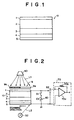
- an electrostatic recording member 10 in accordance with a first aspect of the present invention comprises a first conductive layer 1 which transmits recording radiations L1 such as X-rays (will be referred to as "the recording light L1", hereinbelow), a recording photoconductive layer 2 which exhibits conductivity upon exposure to the recording light L1 passing through the first conductive layer 1, a charge transport layer 3 which substantially acts as an insulator to a charge in the same polarity as a charge placed on the first conductive layer 1 (latent image charge: e.g., a negative charge) and substantially acts as a conductive body to a charge (transfer charge: e.g., a positive charge) in the polarity reverse to the latent image charge, a read-out photoconductive layer 4 which exhibits conductivity upon exposure to a read-out electromagnetic wave L2 (will be referred to as "the read-out light” hereinbelow), and a second conductive layer 5 which transmits the read-out light L2.
- Each of the conductive layers 1 and 5 may comprise, for instance, a glass plate provided with a uniform coating of a conductive material (nesa film or the like).
- the recording photoconductive layer 2 may comprise, for instance, a photoconductive material which contains as a major component at least one of a-Se, lead oxides (II) such as PbO, PbI 2 , and the like, iodine oxides (II), Bi 12 (Ge,Si)O 20 , and Bi 2 I 3 /organic polymer nanocomposites.
- the charge transport layer 3 is as large as possible in the difference between the mobility in the layer of the latent image charge placed on the first conductive layer 1 (e.g., a negative charge) and that of the transfer charge reverse to the latent image charge (e.g., not smaller than 10 2 , preferably not smaller than 10 3 ).
- the charge transport layer 3 may comprise an organic compound such as poly-N-vinylcarbazole (PVK), N,N'-diphenyl-NN'-bis(3-methylphenyl)-[1,1'-biphenyl ]-4,4'-diamine (TPD) and discotic liquid crystal, dispersion of TPD in polymer (polycarbonate, polystyrene, PUK), and a semiconductor material such as a-Se doped with 10 to 200ppm of Cl.
- PVK poly-N-vinylcarbazole
- TPD N,N'-diphenyl-NN'-bis(3-methylphenyl)-[1,1'-biphenyl ]-4,4'-diamine
- PUK polycarbonate, polystyrene, PUK
- semiconductor material such as a-Se doped with 10 to 200ppm of Cl.
- organic compounds are advantageous in that they are insensitive to light and in they are generally low in dielectric constant, which results in reduction in the capacity of the charge transport layer 3 and the read-out photoconductive layer 4 and increase in the signal taking efficiency upon read-out.
- the expression "insensitive to light” means that the material hardly exhibits conductivity upon exposure to the recording light L1 and/or the read-out light L2.
- the read-out photoconductive layer 4 is preferably of a photoconductive material containing as a major component at least one of a-Se, Se-Te, Se-As-Te, nonmetal phthalocyanine and metallophthalocyanine such as MgPc (magnesium phthalocyanine), VoPc (phase II of vanadyl phthalocyanine) and CuPc (copper phthalocyanine).
- a-Se Se-Te
- Se-As-Te Se-As-Te
- nonmetal phthalocyanine and metallophthalocyanine such as MgPc (magnesium phthalocyanine), VoPc (phase II of vanadyl phthalocyanine) and CuPc (copper phthalocyanine).
- the recording photoconductive layer 2 is preferably not smaller than 50 ⁇ m and not larger than 1000 ⁇ m in thickness. In this particular embodiment, the recording photoconductive layer 2 is about 500 ⁇ m in thickness.
- the sum of the thickness of the read-out photoconductive layer 4 and that of the charge transport layer 3 is preferably not larger than 1/2 of the thickness of the recording photoconductive layer 2 and as the sum becomes smaller (not larger than 1/10, 1/20), the response upon read-out (to be described later) is improved.
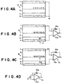
- FIG. 2 is a schematic view showing an electrostatic latent image recording and read-out apparatus using the electrostatic recording member 10.
- the apparatus comprises an electrostatic recording member 10, a recording light projecting means 90, a power source 60, an electric current detecting means 70, a read-out exposure means 92, an on-off switch S1 and a change-over switch S2.
- the recording section is formed by the electrostatic recording member 10, the power source 60, the recording light projecting means 90 and the on-off switch S1
- the read-out section is formed by the electrostatic recording member 10, the current detecting means 70, the read-out exposure means 92 and the change-over switch S2.
- the first conductive layer 1 of the electrostatic recording member 10 is connected to the negative pole of the power source 60 by way of the on-off switch S1 and to the movable contact of the change-over switch S2.
- the change-over switch S2 has a pair of fixed contacts, one connected to the current detecting means 70 and the other grounded.
- the second conductive layer 5 of the electrostatic recording member 10 and the positive pole of the power source 60 are also grounded.
- the current detecting means 70 comprises an operational amplifier (detecting amplifier) 70a and a feedback resistor 70b which form a so-called current/voltage conversion circuit.
- An object 9 having a part 9a transparent to the recording light L1 and a part 9b untransparent to the recording light L1 is placed on the upper surface of the first conductive layer 1 and is uniformly exposed to the recording light L1 by the recording light projecting means 90.
- the read-out exposure means 92 causes the read-out light L2 such as an infrared laser beam to scan the electrostatic recording member 10 in the direction of the arrow in Figure 2. It is preferred that the read-out light L2 scans the electrostatic recording member 10 in the form of a beam spot of a small diameter.
- the recording light L1 is uniformly projected onto the object 9 from the recording light projecting means 90.
- the recording light L1 passes through the transparent portion 9a of the object 9 and the first conductive layer 1 and impinges upon the recording photoconductive layer 2.
- the recording photoconductive layer 2 becomes conductive upon exposure to the recording light L1.
- the resistance of the recording photoconductive layer 2 changes according to the amount of the recording light L1 impinging thereupon due to formation of charged pairs, electrons (negative ⁇ ) and holes (positive ⁇ ), as shown in Figure 3B.
- the resistance of the photoconductive layer 2 becomes smaller.
- the positive charges generated in the recording photoconductive layer 2 travel through the photoconductive layer 2 toward the first conductive layer 1 at a high speed and encounter the negative charges on the first conductive layer 1 at the interface of the first conductive layer 1 and the recording photoconductive layer 2 to be nullified.
- the negative charges generated in the recording photoconductive layer 2 travel through the photoconductive layer 2 toward the charge transport layer 3. Since the charge transport layer 3 acts as an insulating body to the charge which is the same in polarity as the charge placed on the first conductive layer 1 (negative charge in this particular embodiment) as described above, the negative charges travelling toward the charge transport layer 3 are stopped at the interface of the recording photoconductive layer 2 and the charge transport layer 3 and stored there.
- the amount of the stored charges is determined by the amount of negative charges generated in the recording photoconductive layer 2, i.e., the amount of the recording light L1 passing through the object 9.
- the electrostatic latent image recording system for recording to a electrostatic latent image on the electrostatic recording member 10 of the first embodiment can be very simple in structure and the recording operation is very simple.
- the on-off switch S1 is first opened to cut power supply to the electrostatic recording member 10. Then the movable contact of the charge-over switch S2 is connected to the ground to electrify the first and second conductive layers 1 and 5 of the electrostatic recording member 10 at the same potential, thereby rearranging the charges. (See Figure 4A) Thereafter the movable contact of the charge-over switch S2 is switched to the current detecting means 70.
- the read-out light L2 is caused to scan the second conductive layer 5 by the read-out exposure means 92.
- the read-out light L2 passes through the second conductive layer 5 and impinges upon the read-out photoconductive layer 4.
- the read-out photoconductive layer 4 becomes conductive upon exposure to the read-out light L2. This is due to formation of charged pairs, electrons (negative ⁇ ) and holes (positive ⁇ ), as shown in Figure 4B.
- a very strong electric field is established by the stored charges (negative charges) between the second conductive layer 5 and the interface of the read-out photoconductive layer 4 and the charge transport layer 3, and the strength of the electric field increases as the sum of the thicknesses of the read-out photoconductive layer 4 and the charge transport layer 3 becomes smaller. Since the charge transport layer 3 acts as a conductive body to a positive charge, the positive charges generated in the read-out photoconductive layer 4 travel at a high speed through the charge transport layer 3 attracted by the stored charges and encounter the stored charges at the interface of the recording photoconductive layer 2 and the charge transport layer 3 to be nullified.
- the charges can be more surely stored and retainability of the electrostatic latent image can be improved.
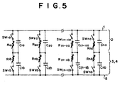
- C *a (* stands for 1, 2 ⁇ ⁇ ⁇ ⁇ , n and basically represents a pixel) represents a distributed capacity in the recording photoconductive layer 2
- C *b (* stands for 1, 2 ⁇ ⁇ ⁇ ⁇ , n and basically represents a pixel) represents a distributed capacity in the charge transport layer 3 and the read-out photoconductive layer 4
- SW *a (* stands for 1, 2 ⁇ ⁇ ⁇ ⁇ , n and basically represents a pixel) represents a photo-switch in the recording photoconductive layer
- SW *b (* stands for 1, 2 ⁇ ⁇ ⁇ ⁇ , n and basically represents a pixel) represents a photo-switch in the charge transport layer 3 and the read-out photoconductive layer 4
- R *a (* stands for 1, 2 ⁇ ⁇ ⁇ ⁇ , n and basically represents a pixel) represents a variable resistor in the recording photoconductive layer 2
- Figure 6 is a view for illustrating the procedure of recording and reading out the electrostatic latent image on the basis of the capacitor model shown in Figure 5 separately for the transparent portion 9a and the untransparent portion 9b of the object 9.
- the distributed capacities C *a and C *b are charged in response to application a DC voltage Ed to the electrostatic recording member 10.
- the photo-switches SW *a are closed in response to exposure to the recording light L1 and the resistances of the variable resistors R *a vary according to the amount of the recording light L1 passing through the first conductive layer 1, whereby only the distributed capacities C *b are held charged.
- This is the electrostatic latent image recording process and the electrostatic latent image is recorded on the distributed capacities C *b .
- the power source 60 is disconnected and the distributed capacities C *b are connected to the distributed capacities C *b , thereby equalizing the potentials of the distributed capacities C *a and C *b .
- the stored charges on the respective portions of the interfaces can be read out in sequence, whereby the electrostatic latent image is read out. Since a very strong electric field is established between the second conductive layer 5 and the interface of the charge transport layer 3 and the recording photoconductive layer 2, the stored charges can be nullified at a very high speed, which results in a very high response in reading out the electrostatic latent image.
- a dark current also flows in proportion to the amount of all the stored charges in addition to the signal current which flows when the stored charges are nullified. Accordingly the signal current is detected riding over the dark current.
- the dark current forms noise in the electrostatic latent image read out.
- the amount of the stored charges is proportional to the intensity of the recording light L1 passing through the object 9. Accordingly when the recording light L1 passing through the object 9 is weak, the amount of stored charges is small and the amount of the dark current is small, whereby the electrostatic latent image read out is high in quality. Further since there hardly remains charge on the electrostatic recording member 10 after the electrostatic latent image is thus read out, another latent image can be recorded on the electrostatic recording member 10 without erasing process.
- the electrostatic recording member 10 of this embodiment may be formed of any suitable materials without limited to those described above.
- the charge transport layer 3 when as the charge transport layer 3, a layer in which the mobility of charge in the direction of thickness of the layer is larger than that in a direction parallel to the layer is employed, the charge is apt to move at a high speed in the direction of thickness of the layer and is not apt to move in the horizontal direction, whereby the sharpness can be improved.
- Preferred materials for forming such a charge transport layer include, for instance, discotic liquid crystals, hexapentyloxytriphenylene (See Physical Review LETTERS 70.4, 1933), and discotic liquid crystals whose core has a ⁇ -conjugation condensed ring or transition metal (See EKISHO, Vol No.1, 1997, P55).
- the charge transport layer 3 includes at least a first charge transport layer formed of a material which substantially acts as an insulator to a charge in the same polarity as a charge placed on the first conductive layer 2 (the latent image charge) and a second charge transport layer formed of a material which substantially acts as a conductive body to a charge in the polarity reverse to the latent image charge (the transfer charge) with the first and second charge transport layers superposed so that the first charge transport layer faces toward the recording photoconductive layer 2 and the second charge transport layer faces toward the read-out photoconductive layer 4, the second charge transport layer contributes to transferring the transfer charge at a high speed and the first charge transport layer acts as a strong insulator to the latent image charge, whereby the charge transport layer can be optimal.
- the first charge transport layer be a layer consisting of at least one of PVK and TPD and the second charge transport layer be an a-Se layer doped with Cl of 10 to 200ppm. In this case, it is preferred that the second charge transport layer is larger in thickness than the first charge transport layer.
- the first and second charge transport layers may be a layer of PVK and a layer of TPD, respectively.
- the charge transport layer may 3 comprise three or more layers.
- the layers should be arranged in the order of insulating force to the latent image charge and the conductivity to the transfer charge so that the insulating force to the latent image charge becomes stronger toward the recording photoconductive layer 2 and the conductivity to the transfer charge becomes higher toward the read-out photoconductive layer 4.
- the read-out photoconductive layer 4 is layer which exhibits a high sensitivity to an electromagnetic wave in a wavelength range of a near ultraviolet region to a blue region (300 to 550nm) and a low sensitivity to an electromagnetic wave in a red region (not shorter than 700nm), the band gap is large and generation of a dark current due to heat can suppressed, whereby noise due to a dark current can be reduced when the read-out light L2 is in a wavelength range of a near ultraviolet region to a blue region.
- the electrostatic recording member 11 of this embodiment differs from that of the first embodiment in that the read-out photoconductive layer 4a is formed of a material which also exhibits conductivity upon exposure to the recording light L1, e.g., a-Se, Se-Te, Se-As and Se-As-Te.
- a method of recording an electrostatic latent image on the electrostatic recording member 11 of this embodiment using the recording and read-out apparatus shown in Figure 2 will be described, hereinbelow. Though the operation of the apparatus is the same as in the electrostatic recording member 10 of the first embodiment, the amount of the charges stored on the interface of the recording photoconductive layer 2 and the charge transport layer 3 when a large amount of recording light L1 is impinges upon the recording photoconductive layer 2 differs from that in the first embodiment. This point will be described in detail, hereinbelow.
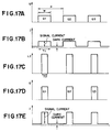
- the amount charges generated in the recording photoconductive layer 2 is substantially proportional to the amount of the recording light L1 impinges upon the photoconductive layer 2 as shown by line a in Figure 7.
- the amount of charges generated in the read-out photoconductive layer 4a is proportional to the amount of the recording light L1, i.e., proportional to the amount of the stored charge, the amount of the stored charges still increase with increase in the amount of the recording light L1.
- the amount of the recording light L1 which reaches the read-out photoconductive layer 4a exceeds a certain value, the amount of the charged pairs generated in the read-out photoconductive layer 4a is sharply increased as shown by line b in Figure 7 by an effect like a so-called avalanche effect. Accordingly in the case of the electrostatic recording member 11 of this embodiment, the amount of the charges stored on the interface is sharply reduced in the range of the amount of the recording light L1 larger than the certain value as shown by line c in Figure 7.
- the amount of the stored charges is kept increased substantially proportional to the amount of the recording light L1 in the same manner as the amount charges generated in the recording photoconductive layer 2 shown by line a in Figure 7.
- the amount of the stored charges linearly changes with the amount of the recording light L1 impinging upon the recording photoconductive layer 2 in a predetermined range of the amount of the recording light L1 (an effective image range).
- the recording light L1 impinges upon in an amount larger than the upper limit of the predetermined range corresponds to a blank portion of the object and does not carry an important image information.
- the amount of the stored charges need not be proportional to the amount of the recording light L1 but it is more important that the charges are not stored in an excessive amount since an excessive amount of the stored charges increases a dark current which deteriorates the S/N ratio of the image read out.
- the stored charges are prevented from being stored in an excessive amount and deterioration in the S/N ratio of the image read out due to the dark current can be prevented.
- the electrostatic recording member 11 of this embodiment can be easily applied to the recording and read-out apparatus shown in Figure 2 by simply replacing the electrostatic recording member 10 of the first embodiment with the electrostatic recording member 11 of this embodiment.
- the electrostatic recording member 12 of this embodiment differs from that of the first embodiment in that a wavelength conversion layer 6 is formed over the first conductive layer 1.
- the wavelength conversion layer 6 is for converting the recording light L1 which is generally X-rays to visible light.
- the wavelength conversion layer 6 is an X-ray scintillator which converts the recording light L1 to blue light L3.
- Such an X-ray scintillator can be formed of caesium iodide (CsI).
- the first conductive layer 1 is transparent to the blue light L3 and the recording photoconductive layer 2 exhibits conductivity upon exposure to the blue light L3. These layers may be the same as those employed in the first and second embodiments. Since the electrostatic recording member 12 of this embodiment is for recording an electrostatic latent image upon exposure to the blue light L3, the first conductive layer 1 need not be transparent to X-rays and the recording photoconductive layer 2 need not be sensitive to X-rays.
- the recording light L1 impinges upon the wavelength conversion layer 6 after passing through the object 9. It is preferred that the wavelength conversion layer 6 is as high as possible in efficiency of converting the recording light L1 to the blue light L3. A layer of CsI is excellent in the wavelength conversion efficiency.
- the blue light L3 passes through the first conductive layer 1 and impinges upon the recording photoconductive layer 2.
- a recording photoconductive layer 2 of amorphous selenium exhibits conductivity at a very high efficiency upon exposure to the blue light L3. Accordingly, substantially the whole blue light L3 contributes to generation of charged pairs in the recording photoconductive layer 2 and a sufficient amount of charges can be stored even if the amount of the recording light L1 is reduced, whereby the dosage to the object can be reduced.
- a layer which converts the recording light L1 to light L4 in a different wavelength range such as a red region in addition to light L3 in the blue region
- a layer formed of a scintillator which is a mixture of phosphors such as Y 2 O 3 :Eu and TVO 4 :Eu emitting red light and phosphors such as CsI emitting blue light is employed as the wavelength conversion layer 6 and a layer which is also sensitive to the red light L4 and exhibits conductivity upon exposure to the red light L4 (e.g., one formed of nonmetal phthalocyanine or metallophthalocyanine) is employed as the read-out photoconductive layer 4, a part of the red light L4 passes through the recording photoconductive layer 2 and the charge transport layer 3 and impinges upon the read-out photoconductive layer 4 since the recording photoconductive layer 2 of amorphous selenium is insensitive to the red light L4.
- a layer which converts the recording light L1 to light L4 in a different wavelength range
- the read-out photoconductive layer 4 becomes conductive upon exposure to the red light L4. Accordingly, the stored charges are prevented from being stored in an excessive amount in the same manner as described above in the second embodiment and deterioration in the S/N ratio of the image read out due to the dark current can be prevented.
- the electrostatic recording member 13 of this embodiment differs from the electrostatic recording member 10 of the first embodiment in that a blocking layer 7a is interposed between the first conductive layer 1 and the recording photoconductive layer 2.
- the blocking layer 7a is a barrier layer which is of Al 2 O 3 or the like about 500 ⁇ thick and has a barrier potential.
- a part of the negative charges placed on the first conductive layer 1 can be directly injected into the recording photoconductive layer 2 and can be stored on the interface of the recording photoconductive layer 2 and the charge transport layer 3. This stored charge component is not derived from exposure to the recording light L1 and accordingly forms noise.
- the blocking layer 7a prevents the charges (negative in this particular embodiment) from being injected into the recording photoconductive layer 2, thereby preventing generation of noise.
- a part of the charges placed on the second conductive layer 5 can be directly injected into the read-out photoconductive layer 4 and can travel through the charge transport layer 3 to encounter the stored charges on the interface of the recording photoconductive layer 2 and the charge transport layer 3.
- a part of the stored negative charges are nullified. This nullification is not derived from exposure to the read-out light L2 and accordingly forms noise.
- a blocking layer 7b is interposed between the second conductive layer 5 and the read-out photoconductive layer 4 in an electrostatic recording member 14 shown in Figure 10B.
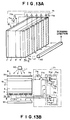
- an electrostatic recording member 15 of this embodiment differs from the electrostatic recording member 10 of the first embodiment in that the second conductive layer 5 is in the form of comb teeth 5a.
- the interspaces 5b between the teeth 5a are filled with a material which is untransparent to the read-out light L2.
- an electrostatic latent image can be recorded on the electrostatic recording member 15 of this embodiment by use of the recording and read-out apparatus shown in Figure 2, charges are stored on the interface between the recording photoconductive layer 2 and the charge transport layer 3 in a manner different from that in the electrostatic recording member 10 of the first embodiment. This will be described with reference to Figures 12A to 12C, hereinbelow.
- a DC voltage is first applied between the first conductive layer 1 and the comb teeth 5a of the second conductive layer 5, thereby electrifying the conductive layers 1 and 5.
- This establishes a U-shaped electric field between the first conductive layer 1 and each comb tooth 5a. Accordingly a substantially parallel electric field exists in the major part of the recording photoconductive layer 2.
- portions Z which are free from an electric field on the interface of the recording photoconductive layer 2 and the charge transport layer 3 between the comb teeth 5a as shown in Figure 12A.
- Such electric field-free portions Z are formed more clearly as the sum of the thicknesses of the charge transport layer 3 and the read-out photoconductive layer 4 becomes smaller as compared with the thickness of the recording photoconductive layer 2 and as the ratio of the width of each comb tooth 5a to the pitch of the teeth 5a becomes smaller (preferably not larger than 75%).
- the electric field-free portions Z are formed more clearly.
- the negative charges are concentrated on the center of each comb teeth 5a and stored on the interface in groups spaced from each other.
- the spaces between the groups of charges correspond to the pitch of the comb teeth 5a and accordingly as the pitch of the comb teeth becomes smaller, the sharpness (space resolution) of the recorded electrostatic latent image increases. It is easy to form the comb teeth 5a at a sufficiently small pitch by use of a semiconductor forming technique.
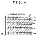
- the recording and read-out apparatus comprises an electrostatic recording member 15, a current detecting means 71, a recording light projecting means 90 and a read-out exposure means 93.
- the read-out exposure means 93 is a line exposure means which causes a line image of a read-out light L2, which is substantially uniform in intensity and extends substantially in perpendicular to the comb teeth 5a, to scan the second conductive layer 5 in the longitudinal direction of the comb teeth 5a.
- the second conductive layer 5 may be scanned with a line image of the read-out light L2 instead of a beam spot and accordingly the scanning optical system may be very simple in structure and can be manufactured at low cost. Further since an incoherent light source can be employed, generation of noise due to interference fringes can be prevented. Of course, the second conductive layer 5 may be scanned with a beam spot.
- the current detecting means 70 comprises a plurality of current detecting amplifiers 71a connected to the comb teeth 5a and detects the electric current flowing through the comb teeth 5a tooth by tooth in parallel.
- the first conductive layer 1 of the electrostatic recording member 15 is connected to one fixed contact of a change-over switch 71b and the negative pole of a power source 71c.
- the positive pole of the power source 71c is connected to the other fixed contact of the change-over switch 71b as shown in Figure 13B.
- An electrostatic latent image is recorded on the electrostatic recording member 15 in the same manner as in the first embodiment.
- the movable contact of the change-over switch 71b is connected to the positive pole of the power source 71c. Thereafter the movable contact of the change-over switch 71b is connected to the first conductive layer 1.
- an electric current I flows to each comb tooth 5a from the first conductive layer 1 through the detecting amplifier 71a.
- an integrating capacitor 71e is charged by the electric current I and charges are stored in the integrating capacitor 71e according to the amount of the current I, whereby the voltage across the integrating capacitor 71e is increased.
- the voltage across the integrating capacitor 71e varies from pixel to pixel according to the stored charges for each pixel.
- the electrostatic latent image can be read out.
- the second conductive layer 5 is in form of a comb electrode, the distributed capacities between the charge transport layer 3 and the read-out photoconductive layer 4 are small and the current detecting means is less apt to be affected by noise. Further the pixel pitch can be fixed to the pitch of the teeth 5a and image data on the electrostatic latent image read out can be corrected depending on the arrangement of the teeth 5a, whereby structure noise can be accurately corrected.
- the positive charges generated in the read-out photoconductive layer 4 upon exposure to the read-out light L2 are more apt to migrate to the interface of the recording photoconductive layer 2 and the charge transport layer 3 to nullify the stored charges, whereby the sharpness can be kept high also upon read-out.
- This effect is significant where there is less charge, that is, portions exposed to less recording light L1.
- the strength of the electric field is increased near the teeth 5a and charged pairs are generated under the strong electric field, the efficiency of ionic dissociation of excitons is increased and quantum efficiency in generation of the charged pairs can be close to 1, whereby the light energy density may be reduced. Further the capacity of the charge transport layer 3 and the read-out photoconductive layer 4 can be reduced and the signal taking efficiency upon read-out can be increased.
- each tooth 5a it is possible to make portions (hatched portions) of each tooth 5a untransparent to the read-out light L2 so that transparent portions and untransparent portions are alternately arranged in the longitudinal direction of the tooth 5a (the scanning direction) as well as making untransparent the interspaces between the teeth 5a.
- the transparent portions are arranged in a grid pattern and pixels adjacent to each other in the longitudinal direction can also be clearly separated, whereby deterioration in space resolution due to interference between the adjacent pixels can be avoided.
- scanning the second conductive layer 5 with a line image of the read-out light L2 results in scanning the read-out photoconductive layer 4 with a plurality of fine beam spots at one time. Accordingly a very high sharpness can be obtained without highly converging the read-out light L2.
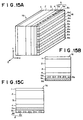
- an electrostatic recording member 16 of this embodiment differs from the electrostatic recording member 15 of the fifth embodiment in that an insulating layer 8c and a third conductive layer 8 provided with a comb teeth conductive portions 8a, both the layers being transparent to the read-out light L2, are superposed on the second conductive layer 5 in this order.
- the comb teeth 8a are substantially in perpendicular to the comb teeth 5a on the second conductive layer 5.
- the stored charges are concentrated on the intersections of the teeth 5a and 8a, whereby an electrostatic latent image can be recorded at a higher sharpness than in the electrostatic recording member 15 of the fifth embodiment.
- the ratio of the width of the tooth 8a to the pitch of the teeth is small (e.g., not larger than 75%), the sharpness can be further increased.
- This effect is further increased by forming the interspaces 8b of the teeth 8a of a material which is untransparent to the read-out light L2, e.g., a high polymer (e.g., polyethylene) dispersed with a small amount of pigment such as carbon black.
- the electrostatic latent image thus recorded can be read out by detecting the electric current flowing between the first conductive layer 1 and the teeth 5a in the same manner as in the fifth embodiment. At this time, it is preferred that the teeth 8a of the third conductive layer 8 be left as it is. Further the pixels can be fixed in the longitudinal directions of the teeth 5a and 8a and structure noise can be more accurately corrected on the basis of the arrangement of the teeth 5a and 8a.
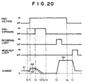
- the read-out exposure means 92 or 93 is assumed to emit steady light. This example differs from the preceding examples in that the read-out exposure means emits the read-out light L2 in a pulse-like fashion. The operation of the read-out apparatus of this example will be described with reference to Figures 17A to 17E, hereinbelow.
- a dark current which is substantially proportional to the total amount of the charges on the pixels flows as described above, and the dark current keeps flowing uniformly irrespective of the pixels while the current is detected and makes a noise component.
- the stored charges Q (Q1 to Q3) for the respective pixels (width W, pitch P) are as shown in Figure 17A
- the currents detected when the stored charges are read out with a reading time of T1 by use of steady read-out light L2 are represented as the sum of the signal current and the dark current proportional to the total amount of the charges as shown in Figure 17B.
- the read-out exposure means emits read-out light L2 of sufficient intensity in a pulse-like fashion (T1>T2) as shown in Figure 17C
- the stored charges are read out only for duration of the pulse light as shown in Figure 17D. Since the current is represented by a time differential of a charge, the shorter the reading time is, the larger the current is for a given amount of charge. Accordingly when the charges are read out with pulse light, a larger current can be detected as shown in Figure 17E.
- FIG. 18 A fifth example of the electrostatic latent image read-out apparatus will be described with reference to Figure 18, hereinbelow.
- the elements analogous to those shown in Figure 2 are given the same reference numerals and will not be described here.
- This example differs from the example shown in Figure 2 only in the arrangement of the current detecting means and the other part of the apparatus are not shown in Figure 18.
- the electrostatic recording member 17 may be any one of the preceding embodiments and the read-out exposure means 95 may be any one of those described above.
- the current detecting means 72 comprises a detecting amplifier (operational amplifier) 72a, an integrating capacitor 72b connected between the output and one input of the operational amplifier 72a, and an on-off switch 72c connected in parallel to the integrating capacitor 72b.
- Said one input of the operational amplifier 72a is connected to the first conductive layer 1 of the electrostatic recording member 17 and the other input is connected to the second conductive layer 5.
- the on-off switch S1 ( Figure 2) is first opened to cut power supply to the electrostatic recording member 17. Then the movable contact of the charge-over switch S2 ( Figure 2) is connected to the ground to electrify the first and second conductive layers 1 and 5 of the electrostatic recording member 10 at the same potential. Thereafter the movable contact of the charge-over switch S2 is switched to the current detecting means 72. This state is shown in Figure 18.
- an electric current I flows from the first conductive layer 1 into the current detecting means 72.
- the integrating capacitor 72b is charged by the electric current I and charges are stored in the integrating capacitor 72b according to the amount of the current I, whereby the voltage across the integrating capacitor 72b is increased. Accordingly, by closing the on-off switch 72c to discharge the stored charges and then opening the on-off switch 72c during intervals between pixels, the voltage across the integrating capacitor 72b varies from pixel to pixel according to the stored charges for each pixel. Thus by detecting the change in the voltage across the integrating capacitor 72b, the electrostatic latent image can be read out.
- the read-out apparatus of this example is equivalent in the effect to that shown in Figure 2 and as simple in structure as that shown in Figure 2.
- FIG. 19 A sixth example of the electrostatic latent image read-out apparatus will be described with reference to Figure 19, hereinbelow.
- the elements analogous to those shown in Figure 2 are given the same reference numerals and will not be described here.
- This example differs from the example shown in Figure 2 only in that a bias power source 73a is inserted between the first conductive layer 1 and input of the current detecting means 73.
- the electrostatic recording member 17 may be any one of the preceding embodiments and the read-out exposure means 95 may be any one of those described above.
- the electrostatic latent image us read out in the same manner as that shown in Figure 2.
- read-out can be effected at a higher speed and the electrostatic latent image can be surely erased. Accordingly, a problem that residual charges generates noise in the following latent image can be avoided.
- the bias power source 73a may be provided separately from the DC power source 60 or the DC power source may double as the bias power source 73a to apply the bias voltage through a suitable switching means such as by changing connection of the switches S1 and S2.
- the pre-exposure is for erasing the unnecessary charges before recording an electrostatic latent image.
- Figure 20 is a timing chart showing the relation among the pre-exposure, exposure to the recording light, exposure to the read-out light, application of a high electric voltage and storage of charge on the electrostatic recording member.
- the residual charge amounts to different values depending on the timing of the pre-exposure.
- the recording light L1 is projected at time t5 after the residual charge is nullified by effecting the pre-exposure from time t2 to time t4 as shown by the solid line in Figure 20
- a charge Q3 bearing thereon only image information can be stored on the electrostatic recording member.
- signals can be taken out on the basis of the Q3 bearing thereon only image information, whereby an afterimage phenomenon and/or deterioration in the S/N ratio can be avoided.
- a recording and read-out apparatus where pre-exposure is effected will be described with reference to Figure 21, hereinbelow.
- This apparatus differs from that shown in Figure 2 only in that a pre-exposure means 96 is provided in addition to the elements shown in Figure 2.
- Predetermined light L2' is projected over the entire area of the second conductive layer 5 of the electrostatic recording member 10 before projecting recording light L1 after application of the high voltage, thereby eliminating the charge stored on the electrostatic recording member 10.
- the pre-exposure may be initiated before application of the high voltage (period from time t0 to t2 in Figure 20.
- the movable contact of the change-over switch S2 is held in its neutral position (where the movable contact is connected to neither of the ground and the current detecting means 70), or in contact with the ground. When grounded, the movable contact should be moved to the neutral position before application of the high voltage.
- the light L2' may of the same electromagnetic wave as the read-out light L2 and may be smaller than the read-out light L2 in amount. Since the pre-exposure is for eliminating the unnecessary charges, the light L2' may be only a particular part of the second conductive layer 5 as required.
- the read-out exposure means 92 may double as the pre-exposure means 96.
- pre-exposure means 96 may comprise an organic or inorganic electric luminescence or a combination of liquid crystal and a back light for the liquid crystal.
- the first conductive layer 1 is electrified in a negative charge and the second or third conductive layer 5 or 8 is electrified in a positive charge, and negative charges are stored on the interface of the recording photoconductive layer 2 and the charge transport layer 3, the conductive layers may be electrified in the reverse charges so that positive charges are stored on the interface.
- the hole transfer layer is changed to an electron transfer layer, and the conductive layers are connected to the reverse poles of the power source upon recording.
- the recording photoconductive layer 2 may comprise a-Se, lead oxides (II), iodine oxides (II) as in the embodiments described above
- the charge transport layer 3 may comprise, for instance, N-trinitrofluoreniden ⁇ aniline(TNFA) derivative, trinitrofluorenone(TNF)/polyester dispersion or nonsymmetrical diphenoquinone derivative
- the read-out photoconductive layer 4 may comprise nonmetal phthalocyanine or metallophthalocyanine as in the embodiments described above
- the read-out photoconductive layer 4a may comprise a-Se, Se-Te, Se-As or Se-As-Te as in the embodiment described above.
- the electrostatic recording member is exposed to the recording radiation from the first conductive layer side. It will be noted, however, that it may be exposed to the recording radiation from the second conductive layer side, when the second conductive layer, the read-out photoconductive layer and the charge transport layer transmit the recording radiation.
Landscapes
- Physics & Mathematics (AREA)
- General Physics & Mathematics (AREA)
- Health & Medical Sciences (AREA)
- Life Sciences & Earth Sciences (AREA)
- High Energy & Nuclear Physics (AREA)
- Molecular Biology (AREA)
- Spectroscopy & Molecular Physics (AREA)
- Measurement Of Radiation (AREA)
- Combination Of More Than One Step In Electrophotography (AREA)
- Photoreceptors In Electrophotography (AREA)
- Radiography Using Non-Light Waves (AREA)
Applications Claiming Priority (6)
| Application Number | Priority Date | Filing Date | Title |
|---|---|---|---|
| JP22211497 | 1997-08-19 | ||
| JP222114/97 | 1997-08-19 | ||
| JP22211497 | 1997-08-19 | ||
| JP21537898 | 1998-07-30 | ||
| JP215378/98 | 1998-07-30 | ||
| JP21537898 | 1998-07-30 |
Publications (2)
| Publication Number | Publication Date |
|---|---|
| EP0898421A2 true EP0898421A2 (fr) | 1999-02-24 |
| EP0898421A3 EP0898421A3 (fr) | 2001-12-05 |
Family
ID=26520846
Family Applications (1)
| Application Number | Title | Priority Date | Filing Date |
|---|---|---|---|
| EP98115539A Withdrawn EP0898421A3 (fr) | 1997-08-19 | 1998-08-18 | Elément d'enregistrement électrostatique, appareil d'enregistrement/reproduction d'images électrostatiques latentes |
Country Status (2)
| Country | Link |
|---|---|
| US (1) | US6268614B1 (fr) |
| EP (1) | EP0898421A3 (fr) |
Cited By (25)
| Publication number | Priority date | Publication date | Assignee | Title |
|---|---|---|---|---|
| JP2001264442A (ja) * | 2000-03-22 | 2001-09-26 | Fuji Photo Film Co Ltd | 画像記録媒体 |
| US6376857B1 (en) | 1998-09-25 | 2002-04-23 | Fuji Photo Film Co., Ltd. | Read-out apparatus for an image detector |
| US6380542B1 (en) | 1998-08-26 | 2002-04-30 | Fuji Photo Film Co., Ltd | Radiation image detecting system |
| EP1136888A3 (fr) * | 2000-03-22 | 2002-07-31 | Fuji Photo Film Co., Ltd. | Medium d' enregistrement d' images et procédé pour sa fabrication |
| US6455857B1 (en) | 1998-08-26 | 2002-09-24 | Fuli Photo Film Co., Ltd. | Radiation image detecting system |
| EP1041401A3 (fr) * | 1999-03-30 | 2002-10-09 | Fuji Photo Film Co., Ltd. | Détecteur de radiation à l'état solide |
| US6469312B2 (en) | 2000-03-31 | 2002-10-22 | Fuji Photo Film Co., Ltd. | Energetic-beam detection apparatus including temperature-controlled selenium detector |
| EP1041400A3 (fr) * | 1999-03-30 | 2002-10-30 | Fuji Photo Film Co., Ltd. | Procédé et dispositif pour enregistrer et reproduire une image radiographique avec un détecteur de rayonnement à l'état solide |
| JP2002329848A (ja) * | 2000-03-22 | 2002-11-15 | Fuji Photo Film Co Ltd | 画像記録媒体およびその製造方法 |
| US6504166B2 (en) | 2000-07-03 | 2003-01-07 | Fuji Photo Film Co., Ltd. | Method and apparatus for recording image in recording medium using photoconductor with reduced dark latent image, and reading image from photoconductor with reduced dark current |
| EP1067401A3 (fr) * | 1999-07-08 | 2003-04-02 | Fuji Photo Film Co., Ltd. | Méthode et dispositif pour enregistrer et lire l'information d'une image |
| US6590224B2 (en) | 2000-03-22 | 2003-07-08 | Fuji Photo Film Co., Ltd. | Image storage medium and method of manufacturing the same |
| US6614045B2 (en) | 2000-04-14 | 2003-09-02 | Fuji Photo Film Co., Ltd. | Imaging apparatus |
| US6627895B2 (en) | 1998-08-28 | 2003-09-30 | Fuji Photo Film Co., Ltd. | Radiation image detecting system |
| US6680483B2 (en) | 2000-04-04 | 2004-01-20 | Fuji Photo Film Co., Ltd. | Image detecting device and readout exposure apparatus therefor |
| US6707059B1 (en) * | 1999-07-22 | 2004-03-16 | Fuji Photo Film Co., Ltd. | Solid state radiation detector |
| EP1400817A1 (fr) * | 2002-09-17 | 2004-03-24 | Fuji Photo Film Co., Ltd. | Capteur d'image radiologique et procédé de production |
| US6756603B2 (en) | 2000-04-14 | 2004-06-29 | Fuji Photo Film Co., Ltd. | Imaging apparatus |
| US6787790B2 (en) | 2000-04-24 | 2004-09-07 | Fuji Photo Film Co., Ltd. | Image information read-out apparatus |
| EP1367448A3 (fr) * | 2002-05-30 | 2004-11-17 | Fuji Photo Film Co., Ltd. | Support d'enregistrement d'image |
| US6838690B2 (en) * | 2001-05-30 | 2005-01-04 | Fuji Photo Film Co., Ltd. | Method and apparatus for recording and reading out an electrostatic latent image |
| EP1342105A4 (fr) * | 2000-11-10 | 2005-09-07 | Hologic Inc | Panneau d'imagerie radiographique directe a imagerie inversement reglable avec une source d'energie externe en application clinique dudit panneau |
| US6975433B2 (en) | 2000-03-31 | 2005-12-13 | Fuji Photo Film Co., Ltd. | Method and apparatus for reading image information |
| EP1538461A3 (fr) * | 2003-11-12 | 2011-03-09 | FUJIFILM Corporation | Procédé et appareil pour la reproduction d'image de rayonnement |
| JP2011185942A (ja) * | 2000-03-22 | 2011-09-22 | Fujifilm Corp | 画像記録媒体およびその製造方法 |
Families Citing this family (73)
| Publication number | Priority date | Publication date | Assignee | Title |
|---|---|---|---|---|
| JP2001211289A (ja) * | 2000-01-27 | 2001-08-03 | Fuji Photo Film Co Ltd | 放射線画像取得方法および装置 |
| JP4356854B2 (ja) * | 2000-03-31 | 2009-11-04 | 富士フイルム株式会社 | 画像信号読取システム及び画像検出器 |
| JP3325881B2 (ja) * | 2000-09-25 | 2002-09-17 | 科学技術振興事業団 | 有機光電流増倍デバイス |
| JP2002350594A (ja) | 2001-05-24 | 2002-12-04 | Fuji Photo Film Co Ltd | 画像記録媒体並びに画像読取方法および装置 |
| JP2002353472A (ja) * | 2001-05-28 | 2002-12-06 | Fuji Photo Film Co Ltd | 光検出装置および方法 |
| US6940084B2 (en) * | 2001-07-04 | 2005-09-06 | Fuji Photo Film Co., Ltd. | Solid state radiation detector |
| JP3785571B2 (ja) * | 2001-11-27 | 2006-06-14 | 富士写真フイルム株式会社 | 固体検出器 |
| JP2003209232A (ja) * | 2002-01-15 | 2003-07-25 | Fuji Photo Film Co Ltd | 固体検出器 |
| JP2003209665A (ja) * | 2002-01-16 | 2003-07-25 | Fuji Photo Film Co Ltd | 画像読取方法および画像記録読取装置 |
| JP2003215736A (ja) * | 2002-01-24 | 2003-07-30 | Fuji Photo Film Co Ltd | 画像撮像装置 |
| JP3766031B2 (ja) * | 2002-01-28 | 2006-04-12 | 富士写真フイルム株式会社 | 画像読取方法および装置 |
| JP3775585B2 (ja) * | 2002-02-08 | 2006-05-17 | 富士写真フイルム株式会社 | 画像記録媒体および製造方法 |
| EP1351094B1 (fr) * | 2002-02-20 | 2006-11-29 | Fuji Photo Film Co., Ltd. | Dispositif pour la reproduction d'image de rayonnement et méthode de reproduction d'image de rayonnement |
| JP3961319B2 (ja) * | 2002-03-15 | 2007-08-22 | 富士フイルム株式会社 | 画像記録媒体およびその製造方法 |
| JP4138405B2 (ja) * | 2002-03-29 | 2008-08-27 | 富士フイルム株式会社 | ライン光源および読取用露光装置 |
| JP4050117B2 (ja) * | 2002-09-17 | 2008-02-20 | 富士フイルム株式会社 | 画像情報記録読取方法および装置 |
| JP4133161B2 (ja) * | 2002-09-20 | 2008-08-13 | 富士フイルム株式会社 | 乳房用画像読取方法および乳房用画像撮像装置 |
| US20040079908A1 (en) * | 2002-10-15 | 2004-04-29 | Fuji Photo Film Co., Ltd. | Radiation detecting cassette |
| JP2004141240A (ja) * | 2002-10-22 | 2004-05-20 | Fuji Photo Film Co Ltd | 放射線検出用カセッテおよび画像情報管理システム |
| EP1416708A1 (fr) * | 2002-10-28 | 2004-05-06 | Fuji Photo Film Co., Ltd. | Procédé et dispositif de lecture d'images |
| JP2004165480A (ja) * | 2002-11-14 | 2004-06-10 | Fuji Photo Film Co Ltd | 画像記録媒体 |
| JP4138458B2 (ja) * | 2002-11-20 | 2008-08-27 | 富士フイルム株式会社 | 放射線画像記録媒体 |
| US8243876B2 (en) | 2003-04-25 | 2012-08-14 | Rapiscan Systems, Inc. | X-ray scanners |
| JP4248929B2 (ja) * | 2003-05-14 | 2009-04-02 | 富士フイルム株式会社 | 放射線検出用カセッテ |
| JP2004344480A (ja) * | 2003-05-23 | 2004-12-09 | Fuji Photo Film Co Ltd | 乳房用画像撮像装置 |
| JP2004361270A (ja) * | 2003-06-05 | 2004-12-24 | Fuji Photo Film Co Ltd | 画像情報読取用露光装置 |
| JP4248940B2 (ja) * | 2003-06-09 | 2009-04-02 | 富士フイルム株式会社 | 放射線検出用カセッテ |
| US7514703B2 (en) | 2003-06-10 | 2009-04-07 | Fujifilm Corporation | Image information detecting cassette |
| JP4053469B2 (ja) * | 2003-06-12 | 2008-02-27 | 富士フイルム株式会社 | 静電潜像読取装置 |
| EP1501275A3 (fr) * | 2003-07-01 | 2005-09-28 | Fuji Photo Film Co., Ltd. | Systeme d'exposition et réseau d'ouverture |
| KR100950668B1 (ko) | 2003-09-30 | 2010-04-02 | 삼성전자주식회사 | 직교 주파수 분할 다중 접속 방식을 사용하는 통신 시스템에서 업링크 파일럿 신호 송수신 장치 및 방법 |
| JP2005123834A (ja) * | 2003-10-16 | 2005-05-12 | Fuji Photo Film Co Ltd | 画像読取方法および装置 |
| JP2005124869A (ja) * | 2003-10-24 | 2005-05-19 | Fuji Photo Film Co Ltd | 乳房用画像撮像装置および検出器ユニット |
| JP2005124868A (ja) * | 2003-10-24 | 2005-05-19 | Fuji Photo Film Co Ltd | X線撮影装置 |
| JP2005134414A (ja) * | 2003-10-28 | 2005-05-26 | Fuji Photo Film Co Ltd | 読取用走査露光装置 |
| JP2005157051A (ja) * | 2003-11-27 | 2005-06-16 | Fuji Photo Film Co Ltd | 直動移動体駆動装置 |
| US7491961B2 (en) * | 2003-12-22 | 2009-02-17 | Fujifilm Corporation | Scanning exposure apparatus, line light source, and image information readout system |
| JP2005310754A (ja) * | 2004-03-24 | 2005-11-04 | Fuji Photo Film Co Ltd | ライン光源および画像情報読取装置 |
| JP2005306722A (ja) * | 2004-03-24 | 2005-11-04 | Fuji Photo Film Co Ltd | 放射線撮像パネルを構成する光導電層の製造方法 |
| JP2005275066A (ja) * | 2004-03-25 | 2005-10-06 | Fuji Photo Film Co Ltd | 走査装置 |
| JP2005285937A (ja) * | 2004-03-29 | 2005-10-13 | Fuji Photo Film Co Ltd | 放射線撮像パネルを構成する光導電層および放射線撮像パネル |
| US7528376B2 (en) * | 2004-08-02 | 2009-05-05 | Fujifilm Corporation | Photo timer and radiographic apparatus |
| JP2006245283A (ja) * | 2005-03-03 | 2006-09-14 | Fuji Photo Film Co Ltd | 画像検出読取装置 |
| JP2006242827A (ja) * | 2005-03-04 | 2006-09-14 | Fuji Photo Film Co Ltd | 放射線固体検出器および放射線固体検出器の試験方法 |
| JP2006261206A (ja) * | 2005-03-15 | 2006-09-28 | Fuji Photo Film Co Ltd | 放射線画像検出器および放射線画像検出システム |
| JP2006280576A (ja) * | 2005-03-31 | 2006-10-19 | Fuji Photo Film Co Ltd | 放射線撮影装置 |
| JP4690106B2 (ja) * | 2005-04-26 | 2011-06-01 | 富士フイルム株式会社 | 放射線画像情報検出方法および放射線画像情報検出装置 |
| JP4738899B2 (ja) | 2005-06-07 | 2011-08-03 | 富士フイルム株式会社 | 画像情報検出装置 |
| JP2007003907A (ja) * | 2005-06-24 | 2007-01-11 | Fujifilm Holdings Corp | 静電記録体 |
| JP2007024611A (ja) * | 2005-07-14 | 2007-02-01 | Fujifilm Holdings Corp | 放射線画像検出方法およびシステム |
| JP2007129347A (ja) * | 2005-11-01 | 2007-05-24 | Fujifilm Corp | 放射線固体検出器の残留電荷消去方法、および放射線画像記録読取装置 |
| US7745806B2 (en) * | 2006-07-07 | 2010-06-29 | Fujifilm Corporation | Solid-state radiation image detector |
| JP2008122500A (ja) * | 2006-11-09 | 2008-05-29 | Fujifilm Corp | 画像情報記録読取方法および装置 |
| US7652258B2 (en) * | 2007-01-08 | 2010-01-26 | Orbotech Medical Solutions Ltd. | Method, apparatus, and system of reducing polarization in radiation detectors |
| JP2008177387A (ja) * | 2007-01-19 | 2008-07-31 | Fujifilm Corp | 放射線画像検出装置 |
| US7787594B2 (en) * | 2007-07-26 | 2010-08-31 | Fujifilm Corporation | Radiation image capturing method, radiation image capturing system and radiation information system for carrying out radiation image capturing method |
| JP4949964B2 (ja) * | 2007-08-10 | 2012-06-13 | 富士フイルム株式会社 | 放射線画像検出器 |
| JP5042757B2 (ja) * | 2007-09-21 | 2012-10-03 | 富士フイルム株式会社 | 放射線画像撮影装置 |
| JP5042756B2 (ja) * | 2007-09-21 | 2012-10-03 | 富士フイルム株式会社 | 放射線画像撮影装置 |
| JP5042760B2 (ja) * | 2007-09-25 | 2012-10-03 | 富士フイルム株式会社 | 放射線画像撮影装置 |
| JP5088947B2 (ja) * | 2007-09-26 | 2012-12-05 | 富士フイルム株式会社 | 放射線画像撮影用カセッテ |
| JP5079438B2 (ja) * | 2007-09-27 | 2012-11-21 | 富士フイルム株式会社 | 放射線画像撮影装置 |
| JP5079439B2 (ja) * | 2007-09-27 | 2012-11-21 | 富士フイルム株式会社 | 放射線画像撮影装置 |
| JP5068128B2 (ja) * | 2007-09-28 | 2012-11-07 | 富士フイルム株式会社 | 放射線画像撮影装置 |
| JP2009088154A (ja) * | 2007-09-28 | 2009-04-23 | Fujifilm Corp | 放射線検出器 |
| JP2009207808A (ja) * | 2008-03-06 | 2009-09-17 | Fujifilm Corp | 放射線画像撮影装置 |
| JP2010037187A (ja) * | 2008-07-10 | 2010-02-18 | Fujifilm Corp | Bi12XO20粉末の製造方法およびBi12XO20粉末、並びに放射線光導電体、放射線検出器および放射線撮像パネル |
| JP2010094209A (ja) * | 2008-10-15 | 2010-04-30 | Fujifilm Corp | 放射線画像撮影装置 |
| JP2010094211A (ja) * | 2008-10-15 | 2010-04-30 | Fujifilm Corp | 放射線画像撮影装置 |
| JP2011194212A (ja) * | 2010-02-24 | 2011-10-06 | Fujifilm Corp | 放射線検出装置 |
| US9954132B2 (en) | 2014-10-29 | 2018-04-24 | General Electric Company | Systems and methods for detectors having improved internal electrical fields |
| US9746565B2 (en) | 2016-01-13 | 2017-08-29 | General Electric Company | Systems and methods for reducing polarization in imaging detectors |
| US9989654B2 (en) | 2016-01-13 | 2018-06-05 | General Electric Company | Systems and methods for reducing polarization in imaging detectors |
Family Cites Families (19)
| Publication number | Priority date | Publication date | Assignee | Title |
|---|---|---|---|---|
| US4176275A (en) | 1977-08-22 | 1979-11-27 | Minnesota Mining And Manufacturing Company | Radiation imaging and readout system and method utilizing a multi-layered device having a photoconductive insulative layer |
| US4521808A (en) * | 1979-03-22 | 1985-06-04 | University Of Texas System | Electrostatic imaging apparatus |
| US4426434A (en) * | 1981-06-23 | 1984-01-17 | Nippon Telegraph & Telephone Public Corp. | Electrophotographic photoreceptor and preparation thereof |
| JPS58182572A (ja) * | 1982-04-20 | 1983-10-25 | Toshiba Corp | 二次元放射線検出器 |
| DE3235076A1 (de) * | 1982-09-22 | 1984-03-22 | Siemens AG, 1000 Berlin und 8000 München | Aufnahme- und auslesevorrichtung fuer roentgenstrahlen |
| DE3236137A1 (de) | 1982-09-29 | 1984-03-29 | Siemens AG, 1000 Berlin und 8000 München | Bildaufnahmeeinrichtung |
| US4542405A (en) * | 1983-06-20 | 1985-09-17 | North American Philips Corporation | Method and apparatus for displaying and reading out an image |
| US4663526A (en) * | 1984-12-26 | 1987-05-05 | Emil Kamieniecki | Nondestructive readout of a latent electrostatic image formed on an insulating material |
| FR2605167B1 (fr) * | 1986-10-10 | 1989-03-31 | Thomson Csf | Capteur d'images electrostatique |
| US4778985A (en) * | 1987-09-14 | 1988-10-18 | Texas Medical Instruments, Inc. | Imaging plate structure |
| US5196702A (en) * | 1987-10-21 | 1993-03-23 | Hitachi, Ltd. | Photo-sensor and method for operating the same |
| CA1276320C (fr) | 1987-12-01 | 1990-11-13 | John Allan Rowlands | Systeme pour mesurer la repartition de la charge en surface d'un photorecepteur |
| JPH03122588A (ja) * | 1989-10-05 | 1991-05-24 | Hitachi Medical Corp | 放射線検出器,データ収集装置およびこれを用いる放射線ct装置 |
| US5268569A (en) | 1992-07-22 | 1993-12-07 | Minnesota Mining And Manufacturing Company | Imaging system having optimized electrode geometry and processing |
| US5556716A (en) * | 1994-08-25 | 1996-09-17 | E. I. Du Pont De Nemours And Company | X-ray photoconductive compositions for x-ray radiography |
| US5759725A (en) * | 1994-12-01 | 1998-06-02 | Kabushiki Kaisha Toshiba | Photoconductors and electrophotographic photoreceptors containing amorphous fullerenes |
| DE69602982T2 (de) * | 1995-03-31 | 1999-10-14 | Fuji Photo Film Co. | Verfahren und Vorrichtung für thermische Aufzeichnung |
| EP0748115A1 (fr) | 1995-06-08 | 1996-12-11 | Agfa-Gevaert N.V. | Procédé pour l'enregistrement et la reproduction d'un modèle de radiation électromagnétique pénétrante |
| US5670291A (en) * | 1996-09-27 | 1997-09-23 | Xerox Corporation | Process for fabricating an electrophotographic imaging member |
-
1998
- 1998-08-18 EP EP98115539A patent/EP0898421A3/fr not_active Withdrawn
- 1998-08-19 US US09/136,739 patent/US6268614B1/en not_active Expired - Fee Related
Cited By (35)
| Publication number | Priority date | Publication date | Assignee | Title |
|---|---|---|---|---|
| US6380542B1 (en) | 1998-08-26 | 2002-04-30 | Fuji Photo Film Co., Ltd | Radiation image detecting system |
| US6455857B1 (en) | 1998-08-26 | 2002-09-24 | Fuli Photo Film Co., Ltd. | Radiation image detecting system |
| US6794655B2 (en) | 1998-08-28 | 2004-09-21 | Fuji Photo Film Co., Ltd. | Radiation image detecting system |
| US6627895B2 (en) | 1998-08-28 | 2003-09-30 | Fuji Photo Film Co., Ltd. | Radiation image detecting system |
| US6376857B1 (en) | 1998-09-25 | 2002-04-23 | Fuji Photo Film Co., Ltd. | Read-out apparatus for an image detector |
| EP1041401A3 (fr) * | 1999-03-30 | 2002-10-09 | Fuji Photo Film Co., Ltd. | Détecteur de radiation à l'état solide |
| US6770901B1 (en) | 1999-03-30 | 2004-08-03 | Fuji Photo Film Co., Ltd. | Radiation solid-state detectors, and radiation image record-reading method and device using the same |
| EP1041400A3 (fr) * | 1999-03-30 | 2002-10-30 | Fuji Photo Film Co., Ltd. | Procédé et dispositif pour enregistrer et reproduire une image radiographique avec un détecteur de rayonnement à l'état solide |
| US6518575B1 (en) | 1999-03-30 | 2003-02-11 | Fuji Photo Film Co., Ltd. | Solid-state radiation detectors |
| EP1067401A3 (fr) * | 1999-07-08 | 2003-04-02 | Fuji Photo Film Co., Ltd. | Méthode et dispositif pour enregistrer et lire l'information d'une image |
| US6707059B1 (en) * | 1999-07-22 | 2004-03-16 | Fuji Photo Film Co., Ltd. | Solid state radiation detector |
| US6617604B2 (en) | 2000-03-22 | 2003-09-09 | Fuji Photo Film Co., Ltd. | Buffer layer for charge storage radiation detector |
| JP2001264442A (ja) * | 2000-03-22 | 2001-09-26 | Fuji Photo Film Co Ltd | 画像記録媒体 |
| US6590224B2 (en) | 2000-03-22 | 2003-07-08 | Fuji Photo Film Co., Ltd. | Image storage medium and method of manufacturing the same |
| US6552356B2 (en) | 2000-03-22 | 2003-04-22 | Fuji Photo Film Co., Ltd. | Image recording medium |
| US6953945B2 (en) | 2000-03-22 | 2005-10-11 | Fuji Photo Film Co., Ltd. | Image recording medium and method of manufacturing the same |
| US6774385B2 (en) | 2000-03-22 | 2004-08-10 | Fuji Photo Film Co., Ltd. | Image recording medium and method of manufacturing the same |
| JP2002329848A (ja) * | 2000-03-22 | 2002-11-15 | Fuji Photo Film Co Ltd | 画像記録媒体およびその製造方法 |
| EP1136888A3 (fr) * | 2000-03-22 | 2002-07-31 | Fuji Photo Film Co., Ltd. | Medium d' enregistrement d' images et procédé pour sa fabrication |
| JP2011185942A (ja) * | 2000-03-22 | 2011-09-22 | Fujifilm Corp | 画像記録媒体およびその製造方法 |
| US6469312B2 (en) | 2000-03-31 | 2002-10-22 | Fuji Photo Film Co., Ltd. | Energetic-beam detection apparatus including temperature-controlled selenium detector |
| US6975433B2 (en) | 2000-03-31 | 2005-12-13 | Fuji Photo Film Co., Ltd. | Method and apparatus for reading image information |
| US6680483B2 (en) | 2000-04-04 | 2004-01-20 | Fuji Photo Film Co., Ltd. | Image detecting device and readout exposure apparatus therefor |
| US6614045B2 (en) | 2000-04-14 | 2003-09-02 | Fuji Photo Film Co., Ltd. | Imaging apparatus |
| EP1146352A3 (fr) * | 2000-04-14 | 2006-03-15 | Fuji Photo Film Co., Ltd. | Appareil pour l'imagerie électrostatique |
| US6756603B2 (en) | 2000-04-14 | 2004-06-29 | Fuji Photo Film Co., Ltd. | Imaging apparatus |
| US6787790B2 (en) | 2000-04-24 | 2004-09-07 | Fuji Photo Film Co., Ltd. | Image information read-out apparatus |
| US6504166B2 (en) | 2000-07-03 | 2003-01-07 | Fuji Photo Film Co., Ltd. | Method and apparatus for recording image in recording medium using photoconductor with reduced dark latent image, and reading image from photoconductor with reduced dark current |
| EP1342105A4 (fr) * | 2000-11-10 | 2005-09-07 | Hologic Inc | Panneau d'imagerie radiographique directe a imagerie inversement reglable avec une source d'energie externe en application clinique dudit panneau |
| US6838690B2 (en) * | 2001-05-30 | 2005-01-04 | Fuji Photo Film Co., Ltd. | Method and apparatus for recording and reading out an electrostatic latent image |
| EP1367448A3 (fr) * | 2002-05-30 | 2004-11-17 | Fuji Photo Film Co., Ltd. | Support d'enregistrement d'image |
| US7214956B2 (en) | 2002-05-30 | 2007-05-08 | Fujifilm Corporation | Image recording medium |
| US7361923B2 (en) | 2002-05-30 | 2008-04-22 | Fujifilm Corporation | Image recording medium |
| EP1400817A1 (fr) * | 2002-09-17 | 2004-03-24 | Fuji Photo Film Co., Ltd. | Capteur d'image radiologique et procédé de production |
| EP1538461A3 (fr) * | 2003-11-12 | 2011-03-09 | FUJIFILM Corporation | Procédé et appareil pour la reproduction d'image de rayonnement |
Also Published As
| Publication number | Publication date |
|---|---|
| EP0898421A3 (fr) | 2001-12-05 |
| US6268614B1 (en) | 2001-07-31 |
Similar Documents
| Publication | Publication Date | Title |
|---|---|---|
| US6268614B1 (en) | Electrostatic recording member, electrostatic latent image recording apparatus, and electrostatic latent image read-out apparatus | |
| JP3445164B2 (ja) | 静電記録体、静電潜像記録装置および静電潜像読取装置 | |
| US6590224B2 (en) | Image storage medium and method of manufacturing the same | |
| US5196702A (en) | Photo-sensor and method for operating the same | |
| US7049601B2 (en) | Image reading method and image recording and reading device | |
| US4857723A (en) | Segmented imaging plate structure | |
| US6953945B2 (en) | Image recording medium and method of manufacturing the same | |
| JP2001264442A (ja) | 画像記録媒体 | |
| US5059794A (en) | Radiation imaging sensor | |
| US4778985A (en) | Imaging plate structure | |
| US7002173B2 (en) | Image recording medium having suppression layer for suppressing interfacial crystallization | |
| US6455867B2 (en) | Image detector having photoconductive layer, linear electrodes transparent to reading light, and signal-readout electrodes shaded from reading light | |
| JP4884593B2 (ja) | 画像記録媒体 | |
| US6566676B1 (en) | Image detector | |
| US6724006B2 (en) | Solid state radiation detector | |
| US6794655B2 (en) | Radiation image detecting system | |
| EP1262797B1 (fr) | Procédé et appareil d'enregistrement d'images et support d'enregistrement | |
| US6949760B2 (en) | Radiation image detector | |
| US6838690B2 (en) | Method and apparatus for recording and reading out an electrostatic latent image | |
| JP2001337171A (ja) | 画像記録媒体およびその製造方法 | |
| US7482614B2 (en) | Radiation image detector | |
| JP2003037258A (ja) | 光検出装置 | |
| JP2011185942A (ja) | 画像記録媒体およびその製造方法 | |
| JP2003101062A (ja) | 静電潜像記録方法および装置 | |
| JP2007053304A (ja) | 放射線画像検出システム |
Legal Events
| Date | Code | Title | Description |
|---|---|---|---|
| PUAI | Public reference made under article 153(3) epc to a published international application that has entered the european phase |
Free format text: ORIGINAL CODE: 0009012 |
|
| AK | Designated contracting states |
Kind code of ref document: A2 Designated state(s): AT BE CH CY DE DK ES FI FR GB GR IE IT LI LU MC NL PT SE Kind code of ref document: A2 Designated state(s): DE FR GB IT NL SE |
|
| AX | Request for extension of the european patent |
Free format text: AL;LT;LV;MK;RO;SI |
|
| PUAL | Search report despatched |
Free format text: ORIGINAL CODE: 0009013 |
|
| AK | Designated contracting states |
Kind code of ref document: A3 Designated state(s): AT BE CH CY DE DK ES FI FR GB GR IE IT LI LU MC NL PT SE |
|
| AX | Request for extension of the european patent |
Free format text: AL;LT;LV;MK;RO;SI |
|
| 17P | Request for examination filed |
Effective date: 20020527 |
|
| AKX | Designation fees paid |
Free format text: DE FR GB IT NL SE |
|
| 17Q | First examination report despatched |
Effective date: 20050517 |
|
| RAP1 | Party data changed (applicant data changed or rights of an application transferred) |
Owner name: FUJIFILM CORPORATION |
|
| STAA | Information on the status of an ep patent application or granted ep patent |
Free format text: STATUS: THE APPLICATION IS DEEMED TO BE WITHDRAWN |
|
| 18D | Application deemed to be withdrawn |
Effective date: 20120215 |