EP0932094A1 - Vorrichtung zur Erzeugung rauscharmer Stromstösse - Google Patents
Vorrichtung zur Erzeugung rauscharmer Stromstösse Download PDFInfo
- Publication number
- EP0932094A1 EP0932094A1 EP99400022A EP99400022A EP0932094A1 EP 0932094 A1 EP0932094 A1 EP 0932094A1 EP 99400022 A EP99400022 A EP 99400022A EP 99400022 A EP99400022 A EP 99400022A EP 0932094 A1 EP0932094 A1 EP 0932094A1
- Authority
- EP
- European Patent Office
- Prior art keywords
- current
- switching
- polarization
- generating
- generation
- Prior art date
- Legal status (The legal status is an assumption and is not a legal conclusion. Google has not performed a legal analysis and makes no representation as to the accuracy of the status listed.)
- Granted
Links
- 230000010287 polarization Effects 0.000 claims abstract description 30
- 230000005540 biological transmission Effects 0.000 claims description 4
- 238000010586 diagram Methods 0.000 description 6
- 230000000694 effects Effects 0.000 description 5
- 230000003071 parasitic effect Effects 0.000 description 5
- 239000000243 solution Substances 0.000 description 5
- 230000008901 benefit Effects 0.000 description 4
- 238000001914 filtration Methods 0.000 description 2
- 238000002347 injection Methods 0.000 description 2
- 239000007924 injection Substances 0.000 description 2
- 238000002955 isolation Methods 0.000 description 2
- 238000004519 manufacturing process Methods 0.000 description 2
- 230000003797 telogen phase Effects 0.000 description 2
- 230000007704 transition Effects 0.000 description 2
- 230000008878 coupling Effects 0.000 description 1
- 238000010168 coupling process Methods 0.000 description 1
- 238000005859 coupling reaction Methods 0.000 description 1
- 230000010354 integration Effects 0.000 description 1
- 238000012423 maintenance Methods 0.000 description 1
- 229910044991 metal oxide Inorganic materials 0.000 description 1
- 150000004706 metal oxides Chemical class 0.000 description 1
- 238000012986 modification Methods 0.000 description 1
- 230000004048 modification Effects 0.000 description 1
- 230000033764 rhythmic process Effects 0.000 description 1
- 239000004065 semiconductor Substances 0.000 description 1
Images

Classifications
-
- G—PHYSICS
- G05—CONTROLLING; REGULATING
- G05F—SYSTEMS FOR REGULATING ELECTRIC OR MAGNETIC VARIABLES
- G05F3/00—Non-retroactive systems for regulating electric variables by using an uncontrolled element, or an uncontrolled combination of elements, such element or such combination having self-regulating properties
- G05F3/02—Regulating voltage or current
- G05F3/08—Regulating voltage or current wherein the variable is DC
- G05F3/10—Regulating voltage or current wherein the variable is DC using uncontrolled devices with non-linear characteristics
- G05F3/16—Regulating voltage or current wherein the variable is DC using uncontrolled devices with non-linear characteristics being semiconductor devices
- G05F3/20—Regulating voltage or current wherein the variable is DC using uncontrolled devices with non-linear characteristics being semiconductor devices using diode- transistor combinations
- G05F3/26—Current mirrors
- G05F3/262—Current mirrors using field-effect transistors only
Definitions
- the field of the invention is that of pulse generation devices for current, also called charge pumps.
- the invention relates to a pulse generation device low noise current.
- the invention applies in particular, but not exclusively, to the generation low noise current pulses for a phase comparator included in a synthesizer of a radiocommunication terminal.
- each device of this type includes means for generation of current pulses, cooperating with polarization means.
- the bias means supply bias voltage to the generating means of current pulses.
- a device for generating current pulses with switched current mirror (cf. FIG. 1) generates current pulses by means of a controlled switching of the switching means ⁇ and ⁇ .
- Such controlled switching is carried out at a frequency which depends on the frequency of the desired pulses.
- two successive phases are implemented. During a first phase, the switching means ⁇ are closed and the switching means ⁇ are open, so as to create at the output (at the source of the transistor means for generating current pulses), a current flow.
- the algebraic value of the current corresponds, for this first type of device, to that of the current leaving the source of the transistor of the biasing means.
- the switching means ⁇ are open and the switching means ⁇ are closed so as to block the flow of current.
- these two phases are repeated at a frequency equal to that sought for the current pulses at output and corresponding to that imposed by the command to open and close the switching means.
- the device for generating current pulses with a cascoded current source (cf. FIG. 2), it generates current pulses by means of controlled switching by the switching means alone. ⁇ .
- Such controlled switching is implemented at a frequency depending on that of the desired pulses.
- the switching means ⁇ are in the open position, this state allows, at the output (at the source of the cascoded transistor), a current flow.
- the switching means ⁇ are in the closed position, so as to block the flow of current at the output.
- these two phases are, as for the first type of device, reiterated at a frequency equal to that sought for the current pulses at output and corresponding to that imposed by the command of the switches.
- the polarization means of these two different types of devices of current pulse generation generate unwanted noise. Indeed, the elements included in these polarization means do not exhibit behavior ideal and therefore generate noise. Such noise (especially that due to the source or sources of current and that due to imperfections of the various elements included in the means of polarization) is recovered by the means for generating current pulses and also transmitted, possibly amplified, downstream of the latter means.
- the biasing means have a feed rejection which is also annoying. In fact, an insufficient feed rejection disturbs the majority of the elements located downstream of the polarization means.
- Another known solution consists in using a logic circuit with low injection of charges.
- this other solution is also not very advantageous because it is difficult compatible with a system whose size is sought to be reduced. Indeed, such logic circuit with low charge injection requires the addition of new elements.
- the present invention aims in particular to overcome these different disadvantages of the state of the art.
- one of the objectives of the present invention is to provide a current pulse generation device allowing its integration into the system that uses it.
- An additional objective of the invention is to provide such a device making it possible to greatly reduce or even eliminate the various noises generated by the polarization means.
- Another object of the invention is to provide such a device allowing its simple manufacturing.
- An additional objective is to provide such a device making it possible to optimize manufacturing costs.
- the general principle of the invention therefore rests on the isolation of the means of polarization with respect to the means for generating current pulses, when a impulse must be generated.
- the invention proposes a simple architecture which can easily be integrated in the system that uses it.
- said polarization means and said means of generation together form a basic structure belonging to the group comprising: a switched current mirror and a cascaded current source.
- the present invention can be implemented in particular with the two large families of current pulse generation devices.
- said basic structure is split, so as to ability to generate positive and / or negative pulses.
- said means of maintenance include at least one capacitive element.
- said means of holding are constituted at least in part by the gate capacitance of a MOS transistor included in said generation means.
- Such a characteristic has the advantage, compared to the first mode of realization, to require no additional components for a basic structure of the cascoded current source type.
- said switching means comprise at least one switching transistor.
- said means for switching further comprises at least one filter resistor connected in parallel on said at least one switching transistor.
- Such a characteristic also makes it possible to reduce the number of pulses necessary to reach the value of the amplitude of the desired current. In other words, this allows faster start-up.
- MOS transistor for "Metal Oxide Semiconductor” in English
- parasitic elements of this transistor prevent ideal switching. It's this resistor mounted in parallel on the switching transistor which largely overcomes to the influences of parasitic elements.
- the invention also relates to a phase comparator comprising a current pulse generation device according to the invention, as mentioned above.
- the present invention relates to a synthesizer comprising a phase comparator according to the invention, as mentioned above.
- the rest phase is advantageously used so that the holding means acquire the bias voltage, with the switching means in closed position.
- the activity phase it benefits from the isolation of the means of maintaining the biasing means with the switching means in position opened.
- the invention therefore relates to a device for generating current pulses. allowing to considerably reduce the influence of the different noises generated by the polarization means in particular on the system which uses it.
- a device for generating current pulses comprises polarization means 31 and means 33 for generating current pulses. These polarization means 31 deliver a polarization voltage to the means 33 for generation of current pulses via switching means 321.
- the means 31 polarization and the generation means 33 together form a basic structure to switched current mirror.
- the polarization means 31 comprise means 311 for creating current and a source 312 of current.
- These current creation means 311 may be a MOS transistor T 1 , the source of which is connected to the supply voltage V DD , the gate is connected to the switching means 321 and the drain is connected to the current source 312.
- the transistor T 1 generates a noise current source 314 of the transistor T 1 and the current source 312 generates a noise current source 313 of the current source 312.
- the generation means 33 comprise means 331 for creating current as well as switching means 322a, 322b.
- the current creation means 331 can be a voltage-controlled MOS transistor T 2 .
- a bias voltage is present at the input (that is to say on the gate of the transistor T2); the transistor T 2 is conducting and the current leaving the source of the transistor T 2 is therefore equal in amplitude to the value of the current passing through the source of the transistor T 1 of the biasing means 31.
- the switching means 322a, 322b are respectively open and closed, the supply voltage V DD is present at the input (on the gate of transistor T 2 ); the transistor T 2 is blocked and the current leaving the drain of the transistor T 2 is canceled. In this way, the switching means 322a, 322b are alternately closed and open to generate a train of current pulses.
- the holding means 34 make it possible to record and keep in memory the bias voltage. It is this bias voltage which allows the control of the current pulse generation means 33.
- the holding means 34 apply the bias voltage at the input of the transistor T 2 , this causes the appearance of an output current at the drain of this transistor T 2 . This generates a current pulse.
- the holding means 34 and the generation means 33 are disconnected from the biasing means 31.
- the generation means 33 can generate one or more non-tainted current pulses of noise from sources 313 and 314 of noise current from transistor T 1 and from the current source.
- the switching means 322a, 322b respectively close and open, the supply voltage is applied to the input of the gate of the transistor T 2 which becomes blocked and no longer lets the current pass. In other words, the drain current of transistor T 2 is canceled and causes the output current to return to zero. This operation is maintained by alternating switching of the means 322a and 322b for switching at the frequency of the desired current pulses.
- the switching means 321, 322a and 322b advantageously comprise each a switching transistor.
- These holding means 34 advantageously comprise at least one element capacitive.
- this basic structure of the switched current mirror type can be duplicated, in a manner known to those skilled in the art, so as to be able to generate positive current pulses and / or negative current pulses.
- a device for generating current pulses comprises polarization means 41 and means 43 for generating current pulses. These polarization means 41 deliver a polarization voltage to the means 43 for generation of current pulses via switching means 421.
- the means 41 polarization and the generation means 43 together form a basic structure to cascoded current source.
- the polarization means 41 comprise means 311 for creating current and a source 312 of current described for the first embodiment.
- these elements namely the MOS transistor T 1 and the current source 312, themselves have parasitic elements which respectively generate a source 314 of noise current from transistor T 1 and a source 313 of noise current from the current source 312.
- the gate and the drain of the transistor T 1 are connected.
- the means 43 for generating comprise means 431 and 432 for creating current as well as means 421 and 422 for switching.
- the means 431 for creating current can be a voltage-controlled MOS transistor T 2 .
- the means 432 for creating current can also be a MOS transistor T 3 .
- the gate of the transistor T 2 is connected to the switching means 421.
- the source of this same transistor T 2 is connected to the supply voltage.
- the drain of transistor T 2 is connected, on the one hand to the source of this transistor T 3 , and on the other hand, to switching means 422.
- the gate of transistor T 3 is connected to a DC voltage supply source delivering a bias voltage.
- the output of this current pulse generation device takes place on the drain of this transistor T 3 .
- the holding means 44 record the bias voltage applied to its terminals. In this way, once the switching means 421 are in the open position, the bias voltage maintained across the terminals of the holding means 44 is applied to the input of the transistor T 2 . This has the effect that the transistor T 2 lets pass the current which is found at the output at the drain of this transistor T 2 .
- the gate of the transistor T 3 being connected to the bias voltage, if the switching means 422 are open, the transistor T 3 turns on. This causes a rise in output current at the drain of transistor T 3 . When the switching means 422 close, the transistor T 3 goes into blocked mode. It follows, at the output, a fallout of the current.
- Such a basic structure can also be split, in a manner known from those skilled in the art, to generate positive and / or negative impulses.
- the switching means 421 and 422 comprise at least one switching transistor and the holding means 44 comprise at least one capacitive element.
- the holding means 44 can also be constituted at least in part by the gate capacitance of the MOS transistor T 2 included in the generating means 431. This has the advantage of saving at least one component, since no additional element is to be added.
- the switching means 421 consist of a switching transistor
- they comprise at least one filter resistor 45 mounted in parallel on this transistor. That is to say, this filter resistor 45 is connected between the drain and the source of the switching transistor.
- this filter resistor 45 is connected between the drain and the source of the switching transistor.
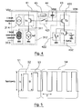
- the relatively small value of the resistor 45 (10 times lower for example than that of R dsoff of the switching transistor) also makes it possible to reduce the value of the equivalent resistance of these two resistors in parallel. Consequently, the current at the output of the transistor increases more in intensity than if the filtering resistor 45 is not present. This has the effect of reducing the number of pulses necessary to obtain a current pulse having a fixed amplitude equal to that of the current pulses of the current pulse train established as illustrated in FIG. 5.
- a train 54 established of current pulses not marred by noise is generated for example by virtue of the variant described above.
- This train 54 established of current pulses has an amplitude I 0 as well as a period T imposed by the rhythm of the switching means 422 (see FIG. 4).
- a transition zone 51 is necessary to reach this stream 54 of current pulses.
- Such a transition zone 51 corresponds to a gradual rise in the amplitudes of the current pulses located in this zone 51.
- a first current pulse 52 and a second current pulse 53 have respectively an amplitude I 1 and I 2 different from that of train 54 established with current pulses I 0 .
- the number is reduced of current pulses 52 and 53 necessary for establishing the amplitude of train 54 of current pulses.
- a device for generating low noise current pulses can be included in the output stage of a phase comparator, itself included in a frequency synthesizer.
- Such a device can for example be used in a terminal radio communication.
- the means 321 or 421 of switching can be in the setting position (closed position).
- these switching means 321 or 421 can be in the position of operation (open position).
Landscapes
- Engineering & Computer Science (AREA)
- Microelectronics & Electronic Packaging (AREA)
- Physics & Mathematics (AREA)
- Nonlinear Science (AREA)
- Electromagnetism (AREA)
- General Physics & Mathematics (AREA)
- Radar, Positioning & Navigation (AREA)
- Automation & Control Theory (AREA)
- Amplifiers (AREA)
- Electronic Switches (AREA)
- Dc-Dc Converters (AREA)
- Manipulation Of Pulses (AREA)
Applications Claiming Priority (2)
| Application Number | Priority Date | Filing Date | Title |
|---|---|---|---|
| FR9800766A FR2774232B1 (fr) | 1998-01-26 | 1998-01-26 | Dispositif de generation d'impulsions de courant a faible bruit, comparateur de phase, synthetiseur et utilisation correspondants |
| FR9800766 | 1998-01-26 |
Publications (2)
| Publication Number | Publication Date |
|---|---|
| EP0932094A1 true EP0932094A1 (de) | 1999-07-28 |
| EP0932094B1 EP0932094B1 (de) | 2003-09-03 |
Family
ID=9522132
Family Applications (1)
| Application Number | Title | Priority Date | Filing Date |
|---|---|---|---|
| EP99400022A Expired - Lifetime EP0932094B1 (de) | 1998-01-26 | 1999-01-07 | Vorrichtung zur Erzeugung rauscharmer Stromstösse |
Country Status (4)
| Country | Link |
|---|---|
| US (1) | US6236252B1 (de) |
| EP (1) | EP0932094B1 (de) |
| DE (1) | DE69910852T2 (de) |
| FR (1) | FR2774232B1 (de) |
Families Citing this family (11)
| Publication number | Priority date | Publication date | Assignee | Title |
|---|---|---|---|---|
| US6415323B1 (en) * | 1999-09-03 | 2002-07-02 | Fastforward Networks | Proximity-based redirection system for robust and scalable service-node location in an internetwork |
| DE10251695A1 (de) * | 2002-11-06 | 2004-05-27 | Infineon Technologies Ag | Stromquellenschaltung zur Erzeugung eines rauscharmen Stroms |
| JP2005173952A (ja) * | 2003-12-11 | 2005-06-30 | Matsushita Electric Ind Co Ltd | 電流源、発光素子駆動回路およびデジタルアナログ変換器 |
| DE10360816A1 (de) * | 2003-12-23 | 2005-07-28 | Deutsche Thomson-Brandt Gmbh | Schaltung und Ansteuerverfahren für eine Leuchtanzeige |
| US9217653B2 (en) * | 2007-09-13 | 2015-12-22 | Rosemount Inc. | High performance architecture for process transmitters |
| DE102010001154A1 (de) * | 2010-01-22 | 2011-07-28 | Robert Bosch GmbH, 70469 | Vorrichtung und Verfahren zur Erzeugung eines Stromimpulses |
| EP2354882B1 (de) * | 2010-02-10 | 2017-04-26 | Nxp B.V. | Umschaltbare Stromquellenschaltung und Verfahren |
| EP2779452B1 (de) * | 2013-03-13 | 2018-08-15 | Nxp B.V. | Umschaltbare Stromquellenschaltung und Verfahren |
| US9541939B2 (en) * | 2014-05-30 | 2017-01-10 | Mediatek Inc. | Switching current source circuit and control method thereof |
| US9641167B2 (en) * | 2014-06-09 | 2017-05-02 | Robert Bosch Gmbh | Current mirror circuits with narrow bandwidth bias noise reduction |
| US10734992B2 (en) * | 2017-08-09 | 2020-08-04 | Infineon Technologies Ag | Circuit and method for providing an output signal |
Citations (3)
| Publication number | Priority date | Publication date | Assignee | Title |
|---|---|---|---|---|
| US5363065A (en) * | 1992-03-18 | 1994-11-08 | U.S. Philips Corporation | Frequency synthesizer utilizing a fast switching current mirror circuit and apparatus comprising such a synthesizer |
| US5461304A (en) * | 1992-05-20 | 1995-10-24 | Siemens Aktiengesellschaft | Switchable current source circuit and phase detector configuration having such a circuit |
| EP0768760A1 (de) * | 1995-10-09 | 1997-04-16 | STMicroelectronics S.r.l. | Stromkomparator |
Family Cites Families (4)
| Publication number | Priority date | Publication date | Assignee | Title |
|---|---|---|---|---|
| GB2209895B (en) * | 1987-09-16 | 1991-09-25 | Philips Electronic Associated | A circuit arrangement for storing sampled analogue electrical currents |
| GB2225912B (en) * | 1988-12-08 | 1993-09-08 | Philips Electronic Associated | Current mirror circuit |
| GB2235799A (en) * | 1989-09-06 | 1991-03-13 | Philips Electronic Associated | Differentiator circuit |
| US6021162A (en) * | 1997-10-01 | 2000-02-01 | Rosemount Inc. | Vortex serial communications |
-
1998
- 1998-01-26 FR FR9800766A patent/FR2774232B1/fr not_active Expired - Lifetime
-
1999
- 1999-01-07 DE DE69910852T patent/DE69910852T2/de not_active Expired - Lifetime
- 1999-01-07 EP EP99400022A patent/EP0932094B1/de not_active Expired - Lifetime
- 1999-01-25 US US09/236,114 patent/US6236252B1/en not_active Expired - Lifetime
Patent Citations (3)
| Publication number | Priority date | Publication date | Assignee | Title |
|---|---|---|---|---|
| US5363065A (en) * | 1992-03-18 | 1994-11-08 | U.S. Philips Corporation | Frequency synthesizer utilizing a fast switching current mirror circuit and apparatus comprising such a synthesizer |
| US5461304A (en) * | 1992-05-20 | 1995-10-24 | Siemens Aktiengesellschaft | Switchable current source circuit and phase detector configuration having such a circuit |
| EP0768760A1 (de) * | 1995-10-09 | 1997-04-16 | STMicroelectronics S.r.l. | Stromkomparator |
Also Published As
| Publication number | Publication date |
|---|---|
| US6236252B1 (en) | 2001-05-22 |
| FR2774232A1 (fr) | 1999-07-30 |
| DE69910852T2 (de) | 2004-07-15 |
| DE69910852D1 (de) | 2003-10-09 |
| FR2774232B1 (fr) | 2000-02-25 |
| EP0932094B1 (de) | 2003-09-03 |
Similar Documents
| Publication | Publication Date | Title |
|---|---|---|
| EP0932094B1 (de) | Vorrichtung zur Erzeugung rauscharmer Stromstösse | |
| EP0562904B1 (de) | Verfahren und Vorrichtung zur Regelung einer Verzögerung über mehrere Verzögerungsbereiche | |
| FR2882871A1 (fr) | Oscillateur commande en tension a multiphase realignee et boucle a phase asservie associee | |
| EP0568422B1 (de) | Spannungskomparator mit sehr kleinem Verbrauch | |
| EP1085659A1 (de) | Digital-Analog-Wandler des Stromtyps | |
| EP0562905B1 (de) | Schaltung mit veränderlicher Verzögerung | |
| FR2473814A1 (fr) | Circuit mos dynamique ne dependant pas d'un rapport de resistances destine a constituer des circuits logiques divers | |
| EP0901227B1 (de) | Schaltung mit variabler Verzögerung | |
| FR2774234A1 (fr) | Dispositif a semiconducteur | |
| EP0667677A1 (de) | Anordnung zur Multiplizierung einer Kapazität mit einem variierbarem Koeffizienten zur Grenzfrequenzregulung eines Filters und Filter mit einer derartigen Anordnung | |
| FR3059498A1 (fr) | Procede et circuit de commande d'un dispositif de commutation d'un circuit de puissance | |
| FR2865586A1 (fr) | Detecteur de phase/frequence de boucle a phase asservie avec pompe a charge de sortie completement differentielle | |
| FR2722625A1 (fr) | Convertisseur a/n a comparaison multiple utilisant le principe d'interpolation | |
| EP0537083B1 (de) | Vorrichtung zum Lesen eines Speicherzelleinhalts, insbesondere für ein EPROM, Betriebsverfahren und Speicher mit einer solchen Vorrichtung | |
| FR2744304A1 (fr) | Convertisseur numerique-analogique differentiel a fonction de filtrage et compensation de decalage | |
| EP0899921B1 (de) | Symmetrischer Leitungstreiber | |
| EP4350992B1 (de) | Analog-zeit-wandler | |
| FR2618962A1 (fr) | Porte " ou exclusif " en technologie cmos | |
| EP1371139A2 (de) | Rauscharme ladungspumpe für eine phasenregelschleife | |
| EP2777045B1 (de) | Schaltungsanordnung zur vorspannung der invertern-wannen zur reduzierung des energieverbrauchs eines srams | |
| CH691018A5 (fr) | Oscillateur fonctionnant avec une faible tension d'alimentation. | |
| FR2879858A1 (fr) | Procede de correction du dephasage entre deux signaux d'enree d'une boucle a verrouillage de phase et dispositif associe | |
| EP0772359A1 (de) | Filtervorrichtung zur Verarbeitung einer Vielzahl von Kanälen in einem Kabelfernsehverteilungssystem | |
| FR2905043A1 (fr) | Circuit bistable a basculement d'etat auto-ajuste temporellement et bascule flip-flop utilisant un tel circuit bistable. | |
| EP0349028A2 (de) | Integrierte Halbleiterschaltung mit einem differentiellen Paar von FETs |
Legal Events
| Date | Code | Title | Description |
|---|---|---|---|
| PUAI | Public reference made under article 153(3) epc to a published international application that has entered the european phase |
Free format text: ORIGINAL CODE: 0009012 |
|
| AK | Designated contracting states |
Kind code of ref document: A1 Designated state(s): DE GB IE IT |
|
| AX | Request for extension of the european patent |
Free format text: AL;LT;LV;MK;RO;SI |
|
| 17P | Request for examination filed |
Effective date: 20000128 |
|
| AKX | Designation fees paid |
Free format text: DE GB IE IT |
|
| GRAH | Despatch of communication of intention to grant a patent |
Free format text: ORIGINAL CODE: EPIDOS IGRA |
|
| GRAS | Grant fee paid |
Free format text: ORIGINAL CODE: EPIDOSNIGR3 |
|
| GRAA | (expected) grant |
Free format text: ORIGINAL CODE: 0009210 |
|
| AK | Designated contracting states |
Kind code of ref document: B1 Designated state(s): DE GB IE IT |
|
| PG25 | Lapsed in a contracting state [announced via postgrant information from national office to epo] |
Ref country code: IE Free format text: LAPSE BECAUSE OF FAILURE TO SUBMIT A TRANSLATION OF THE DESCRIPTION OR TO PAY THE FEE WITHIN THE PRESCRIBED TIME-LIMIT Effective date: 20030903 |
|
| REG | Reference to a national code |
Ref country code: GB Ref legal event code: FG4D Free format text: NOT ENGLISH |
|
| GBT | Gb: translation of ep patent filed (gb section 77(6)(a)/1977) | ||
| REF | Corresponds to: |
Ref document number: 69910852 Country of ref document: DE Date of ref document: 20031009 Kind code of ref document: P |
|
| REG | Reference to a national code |
Ref country code: IE Ref legal event code: FG4D Free format text: FRENCH |
|
| REG | Reference to a national code |
Ref country code: IE Ref legal event code: FD4D |
|
| PLBE | No opposition filed within time limit |
Free format text: ORIGINAL CODE: 0009261 |
|
| STAA | Information on the status of an ep patent application or granted ep patent |
Free format text: STATUS: NO OPPOSITION FILED WITHIN TIME LIMIT |
|
| 26N | No opposition filed |
Effective date: 20040604 |
|
| REG | Reference to a national code |
Ref country code: GB Ref legal event code: 732E |
|
| REG | Reference to a national code |
Ref country code: GB Ref legal event code: 732E Free format text: REGISTERED BETWEEN 20090924 AND 20090930 |
|
| REG | Reference to a national code |
Ref country code: GB Ref legal event code: 732E Free format text: REGISTERED BETWEEN 20120607 AND 20120613 |
|
| PGFP | Annual fee paid to national office [announced via postgrant information from national office to epo] |
Ref country code: GB Payment date: 20161228 Year of fee payment: 19 |
|
| PGFP | Annual fee paid to national office [announced via postgrant information from national office to epo] |
Ref country code: DE Payment date: 20180122 Year of fee payment: 20 |
|
| PGFP | Annual fee paid to national office [announced via postgrant information from national office to epo] |
Ref country code: IT Payment date: 20180129 Year of fee payment: 20 |
|
| GBPC | Gb: european patent ceased through non-payment of renewal fee |
Effective date: 20180107 |
|
| PG25 | Lapsed in a contracting state [announced via postgrant information from national office to epo] |
Ref country code: GB Free format text: LAPSE BECAUSE OF NON-PAYMENT OF DUE FEES Effective date: 20180107 |
|
| REG | Reference to a national code |
Ref country code: DE Ref legal event code: R071 Ref document number: 69910852 Country of ref document: DE |