EP0902443B1 - Agencement de bobines planaire couplé - Google Patents
Agencement de bobines planaire couplé Download PDFInfo
- Publication number
- EP0902443B1 EP0902443B1 EP19980116465 EP98116465A EP0902443B1 EP 0902443 B1 EP0902443 B1 EP 0902443B1 EP 19980116465 EP19980116465 EP 19980116465 EP 98116465 A EP98116465 A EP 98116465A EP 0902443 B1 EP0902443 B1 EP 0902443B1
- Authority
- EP
- European Patent Office
- Prior art keywords
- coil
- coils
- conductor track
- plane
- conductor
- Prior art date
- Legal status (The legal status is an assumption and is not a legal conclusion. Google has not performed a legal analysis and makes no representation as to the accuracy of the status listed.)
- Expired - Lifetime
Links
- 239000004020 conductor Substances 0.000 claims description 40
- 230000008878 coupling Effects 0.000 claims description 13
- 238000010168 coupling process Methods 0.000 claims description 13
- 238000005859 coupling reaction Methods 0.000 claims description 13
- 238000002955 isolation Methods 0.000 claims description 3
- 238000001465 metallisation Methods 0.000 claims description 3
- 238000010079 rubber tapping Methods 0.000 claims 1
- 239000011162 core material Substances 0.000 description 3
- 101100379079 Emericella variicolor andA gene Proteins 0.000 description 1
- 230000001419 dependent effect Effects 0.000 description 1
- 238000011161 development Methods 0.000 description 1
- 230000018109 developmental process Effects 0.000 description 1
- 230000005294 ferromagnetic effect Effects 0.000 description 1
- 230000006698 induction Effects 0.000 description 1
- 230000005291 magnetic effect Effects 0.000 description 1
- 239000000758 substrate Substances 0.000 description 1
Images


Classifications
-
- H—ELECTRICITY
- H01—ELECTRIC ELEMENTS
- H01F—MAGNETS; INDUCTANCES; TRANSFORMERS; SELECTION OF MATERIALS FOR THEIR MAGNETIC PROPERTIES
- H01F17/00—Fixed inductances of the signal type
- H01F17/0006—Printed inductances
- H01F17/0013—Printed inductances with stacked layers
Definitions
- the invention relates to a planar, coupled coil arrangement which can be used, for example, in an oscillator or a bandpass filter. It can also serve, for example, as a transformer, as an impedance converter, for coupling amplifier stages or for galvanic isolation.
- a coil is a device that can store electromagnetic energy.
- the coil is defined by constructive data of the coil such as length, diameter, shape, number of turns, core material and core shape.
- JP 06 013239 A discloses a pair of two coils respectively arranged in sections on the front and rear sides of an insulating film.
- EP 0 371 157 A discloses a power transformer with coil-shaped elements for coupling an antenna of a magnetic resonance tomograph.
- An object of the invention is to provide a planar, coupled coil arrangement in which the disadvantages of the prior art are avoided.
- the planar, coupled coil arrangement has a first coil, in which a first conductor portion of the first coil is arranged in a first plane and the first coil completion portion is arranged in a second plane and electrically connected by one or more connections to the first conductor portion connected is.
- a second coil is provided, in which the conductor track is arranged wholly or partly in the second plane, in which if the second coil is arranged partially in the second plane, the part of the conductor track in the first or the second coil completing the second coil arranged third level and is electrically connected by one or more connections with the first conductor part of the second coil.
- the coils are arranged symmetrically to each other and arranged the conductor tracks of the coils to each other so that a coupling between the coils takes place. Furthermore, the planes in which the conductor tracks and conductor track parts of the coils are arranged, metallization layers of an integrated circuit.
- a third coil may be provided, in which the conductor track is arranged wholly or partly in the third plane and, if the conductor track of the third coil is arranged partially in the third plane, the part of the conductor track in the first completing the third coil or the second level and is electrically connected by one or more connections to the first conductor portion of the third coil.
- the coil leads may have coil taps which are electrically connected by one or more connections to the trace of the respective coil.
- the coils can be made round. This has the advantage that an optimal coupling between the coils can be achieved.
- the coils can also be made square. This has the advantage of easy manufacturability.
- the coils are arranged around the circuit. This saves space.
- planar, coupled coil arrangement according to the invention is advantageously usable in an oscillator, in a bandpass filter, as a transformer, as an impedance converter, for coupling amplifier stages or for galvanic isolation.
- FIG. 1 shows a first embodiment of the coil arrangement according to the invention with a first embodiment of the resistance circuit.
- FIG. 2 shows the first embodiment of the coil assembly according to the invention with a second embodiment of the resistance circuit.
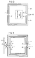
- FIG. 3 shows a first plane of a second embodiment of the coil assembly according to the invention.
- FIG. 4 shows the second level of the second embodiment of the coil assembly according to the invention.
- FIG. 5 shows the third level of the second embodiment of the coil assembly according to the invention.
- FIG. 6 shows a third embodiment of the coil arrangement according to the invention in plan view.
- FIG. 7 shows the third embodiment of the coil assembly according to the invention in a three-dimensional view.
- FIG. 8 shows a fourth embodiment of the coil assembly according to the invention in a three-dimensional view.
- FIG. 9 shows a fifth embodiment of the coil assembly according to the invention in a three-dimensional view.
- FIG. 10 shows a sixth embodiment of the coil assembly according to the invention in a three-dimensional view.
- two coils S1 and S2 are present, which are connected via a resistor R1 to a conductor L1, which may for example lead to a reference potential.
- the black drawn areas of the coils S1 and S2 are in a first plane.
- the connections V1 and V2 are in a second plane and connect the conductor ends A, B and A ', B' together.
- the connections between the first level and the second level at the points A, B, A 'and B' can be made, for example, by plated-through holes.
- the coil terminals of the coils S1 and S2 are labeled A1, A2 and A3.
- connection A3 for the coils S1 and S2 can also separate ports A3 and A4 for the coils S1 and S2, respectively FIG. 2 be provided.
- the coils S1 and S2 are connected to the resistor R1 via the resistors R2 and R3, respectively.
- resistors R1, R2 and R3 instead of the resistors R1, R2 and R3, other circuit elements can be connected to the coils S1 and S2.
- FIG. 3 is the lowest level (Alu1) closest to the substrate. Arranged above is the second plane (Alu2) shown in FIG. 4, and in turn the latter in FIG. 5 shown top level (Alu3).
- the conductor L1 to which the coils S1 and S2 are connected can be connected to a reference potential.
- the coils S1 and S2 according to FIG. 4 and 5 have two ports A1 and A2, and a common port A3.
- the conductor L1 be connected to the terminal A3.
- the terminal A3 may also be connected to a circuit element.
- the conductor ends A '''', B '''' and A ''',B''' in FIG. 4 are each a conductor track section, which between the points A '''', B '''andA''', B '''according to FIG. 5 is located, and corresponding vias interconnected.
- the points A ", B" and A, B in FIG FIG. 5 with the between the points A '', B '' and A, B according to FIG. 4 located interconnects and corresponding vias connected.
- the connecting element V which also represents a conductor track and between the points A ', B' in FIG. 4 is used to bridge the trace in FIG. 3 between points A 'and B'.
- the conductor V is part of the coils S3 and S4 according to FIG. 3 ,
- the coils S3 and S4 have a common terminal A6, and one terminal A5 and A4, respectively.
- a circuit may be provided within these coils. This has, first, the advantage that space can be saved and, second, that in order to get from the circuit to the terminals A4 and A5 no additional bridges for bridging the tracks of the coils S3 and S4 are necessary.
- the two coils S1 and S2 are predominantly one above the other. While the coil S1 predominantly in the is located first level, the coil S2 is located predominantly in the second level. The first level is gray, the second level is black.
- the coil S1 has the terminals A1 and A2.
- the ports A3 and A4 belong to the coil S2.
- the coils S1 and S2 are shown in three-dimensional view.
- the coil S2 is located directly below the coil S1.
- connections in the second plane are provided, which serve to bridge the running between the points A and B in the first plane conductor of the first coil S1.
- a connection between the points A 'and B' is provided in the first plane, which serves for bridging the between the points A 'and B' extending conductor track in the second plane.
- the connections are connected to corresponding vias with the respective tracks of the coils.
- the coupling of the coils S1 and S2 takes place transversely to the two planes.
- the coils S1 and S2 are symmetrical to one another.
- FIG. 8 shown fourth embodiment of the coil assembly on another coil S3, which is located in a third plane.
- the coil S3 has the terminals A5 and A6.
- the coil S3 is also coupled transversely to the planes 1, 2 and 3 with the coils S1 and S2.
- the coils S1 and S2 represent bifilar coils.
- Coil taps for example, as in FIG. 9 shown to be executed.
- leads C, D and E are provided with the corresponding terminals A7, A8 and A9. While the turns of the coils are on the upper level, the leads C, D and E and the junctions between the points A, B and A ', B' are provided on the lower level. The coupling takes place here within the plane.
- the coupling between the coils S1 and S2 or the coils S3 and S2 takes place vertically, ie transversely to the planes, while the coupling between the coils S1 and S3 takes place in the plane.
- the coil S1 has the terminals A1 and A2, the coil S2, the terminals A3, A7 and A4, and the coil S3, the terminals A5 and A6.
- the terminal A7 represents a center tap of the coil S2.
- the connection between the points A and B of the coil S2 is provided in a third plane.
- all embodiments of the coil arrangement according to the invention are both angular and round executable.
- the coil arrangement according to the invention is also optimized in such a way that the number of required metallization layers in the integrated circuit are minimized.
Landscapes
- Engineering & Computer Science (AREA)
- Power Engineering (AREA)
- Microelectronics & Electronic Packaging (AREA)
- Coils Or Transformers For Communication (AREA)
Claims (8)
- Agencement de bobines planaire couplé,
comprenant une première bobine (S1)
dans laquelle une première partie de piste conductrice de la première bobine (S1) est disposée dans un premier plan,
dans laquelle une partie de piste conductrice complétant la première bobine (S1) est disposée dans un deuxième plan et est reliée électriquement à la première partie de piste conductrice par une liaison ou par plusieurs liaisons,
comprenant une deuxième bobine (S2),
dans laquelle la piste conductrice est disposée entièrement ou en partie dans le deuxième plan,
dans laquelle, dans le cas où la piste conductrice de la deuxième bobine (S2) est disposée en partie dans le deuxième plan, la partie de la piste conductrice complétant la deuxième bobine (S2) est disposée dans le premier plan ou dans un troisième plan et est reliée électriquement à la première partie de piste conductrice de la deuxième bobine (S2) par une liaison ou par plusieurs liaisons,
dans lequel les bobines (S1, S2) sont disposées symétriquement l'une par rapport à l'autre,
dans lequel les pistes conductrices des bobines (S1, S2) sont disposées les unes par rapport aux autres de manière à ce qu'un couplage entre les bobines (S1, S2) ait lieu,
et dans lequel les plans dans lesquels les pistes conductrices et les parties de piste conductrice des bobines (S1, S2) sont disposées sont des couches de métallisation d'un circuit intégré. - Agencement de bobines suivant la revendication 1,
comprenant une troisième bobine (S3), dans laquelle la piste conductrice est disposée complètement ou en partie dans le troisième plan,
dans lequel, dans le cas où la troisième bobine (S3) est disposée en partie dans le troisième plan, la partie de la piste conductrice complétant la piste conductrice de la troisième bobine (S3) est disposée dans le premier ou dans le deuxième plan et est reliée électriquement à la première partie de piste conductrice de la troisième bobine (S3) par une liaison ou par plusieurs liaisons. - Agencement de bobines suivant l'une des revendications 1 ou 2, dans lequel il est prévu pour la prise de bobine, des pistes (C, D, E) conductrice de connexion, qui sont reliées électriquement à la piste conductrice de la bobine correspondante par une liaison ou par plusieurs liaisons.
- Agencement de bobines suivant l'une des revendications 1 à 3, dans laquelle les bobines (S1, S2, S3) sont rondes.
- Agencement de bobines suivant l'une des revendications 1 à 3, dans lequel les bobines ((S1, S2, S3) sont polygonales.
- Agencement de bobines suivant l'une des revendications 1 à 5, dans lequel les bobines sont disposées autour du circuit.
- Agencement de bobines suivant l'une des revendications 1 à 6, dans lequel les pistes conductrices des bobines sont disposées d'une manière prépondérante les unes sur les autres.
- Utilisation de l'agencement de bobines suivant l'une des revendications 1 à 7, dans un oscillateur, dans un passe-bande, comme transformateur, comme convertisseur d'impédance, pour le couplage d'étages d'amplificateur ou pour la séparation galvanique.
Applications Claiming Priority (2)
| Application Number | Priority Date | Filing Date | Title |
|---|---|---|---|
| DE1997139962 DE19739962C2 (de) | 1997-09-11 | 1997-09-11 | Planare, gekoppelte Spulenanordnung |
| DE19739962 | 1997-09-11 |
Publications (3)
| Publication Number | Publication Date |
|---|---|
| EP0902443A2 EP0902443A2 (fr) | 1999-03-17 |
| EP0902443A3 EP0902443A3 (fr) | 1999-09-08 |
| EP0902443B1 true EP0902443B1 (fr) | 2009-03-11 |
Family
ID=7842025
Family Applications (1)
| Application Number | Title | Priority Date | Filing Date |
|---|---|---|---|
| EP19980116465 Expired - Lifetime EP0902443B1 (fr) | 1997-09-11 | 1998-09-01 | Agencement de bobines planaire couplé |
Country Status (2)
| Country | Link |
|---|---|
| EP (1) | EP0902443B1 (fr) |
| DE (2) | DE19739962C2 (fr) |
Cited By (1)
| Publication number | Priority date | Publication date | Assignee | Title |
|---|---|---|---|---|
| EP3367067A1 (fr) | 2017-02-28 | 2018-08-29 | Melexis Technologies SA | Capteur de position et procédé de détection de position |
Families Citing this family (10)
| Publication number | Priority date | Publication date | Assignee | Title |
|---|---|---|---|---|
| DE19756188A1 (de) * | 1997-12-17 | 1999-06-24 | Trw Nelson Bolzenschweisstechn | Leistungsübertrager für ein Leistungsschaltnetzteil, insbesondere für Bolzenschweißgeräte |
| DE19960474B4 (de) * | 1999-12-15 | 2004-07-01 | Forschungszentrum Jülich GmbH | Transformator |
| KR100420948B1 (ko) * | 2001-08-22 | 2004-03-02 | 한국전자통신연구원 | 병렬 분기 구조의 나선형 인덕터 |
| US6803849B2 (en) * | 2002-10-31 | 2004-10-12 | Intersil Americas Inc. | Solid state inducting device |
| CN1299303C (zh) * | 2004-01-30 | 2007-02-07 | 联华电子股份有限公司 | 对称型电感 |
| CN101017726B (zh) * | 2004-01-30 | 2011-07-27 | 联华电子股份有限公司 | 对称型电感 |
| CN100416797C (zh) * | 2006-09-19 | 2008-09-03 | 威盛电子股份有限公司 | 对称电感元件 |
| CN100565875C (zh) * | 2007-10-26 | 2009-12-02 | 威盛电子股份有限公司 | 对称电感元件 |
| JP2011040509A (ja) | 2009-08-07 | 2011-02-24 | Imec | 2層式トランス |
| CN114496500A (zh) * | 2020-10-26 | 2022-05-13 | 北京小米移动软件有限公司 | 一种充电线圈结构、接收端、发送端及无线充电系统 |
Family Cites Families (9)
| Publication number | Priority date | Publication date | Assignee | Title |
|---|---|---|---|---|
| DE7515106U (de) * | 1975-05-10 | 1976-02-19 | Blaupunkt-Werke Gmbh, 3200 Hildesheim | Gedruckte spule |
| DE8226746U1 (de) * | 1982-09-23 | 1983-04-14 | Schwär, Gerhard, 2070 Ahrensburg | Transformator |
| DE3888185D1 (de) * | 1988-11-28 | 1994-04-07 | Siemens Ag | Leitungstransformator. |
| JPH0377360A (ja) * | 1989-08-18 | 1991-04-02 | Mitsubishi Electric Corp | 半導体装置 |
| JP3141562B2 (ja) * | 1992-05-27 | 2001-03-05 | 富士電機株式会社 | 薄膜トランス装置 |
| JPH0613239A (ja) * | 1992-06-25 | 1994-01-21 | Matsushita Electric Works Ltd | 平面形トランス |
| DE807941T1 (de) * | 1994-08-24 | 1998-03-26 | Yokogawa Electric Corp | Gedruckte Spule |
| EP0771012A3 (fr) * | 1994-08-24 | 1998-02-25 | Yokogawa Electric Corporation | Transformateur à bobines imprimées |
| DE19522043A1 (de) * | 1995-06-17 | 1996-12-19 | Bosch Gmbh Robert | Induktives Bauelement |
-
1997
- 1997-09-11 DE DE1997139962 patent/DE19739962C2/de not_active Expired - Fee Related
-
1998
- 1998-09-01 DE DE59814350T patent/DE59814350D1/de not_active Expired - Lifetime
- 1998-09-01 EP EP19980116465 patent/EP0902443B1/fr not_active Expired - Lifetime
Cited By (2)
| Publication number | Priority date | Publication date | Assignee | Title |
|---|---|---|---|---|
| EP3367067A1 (fr) | 2017-02-28 | 2018-08-29 | Melexis Technologies SA | Capteur de position et procédé de détection de position |
| US10415997B2 (en) | 2017-02-28 | 2019-09-17 | Melexis Technologies Sa | Position sensor and method of position sensing |
Also Published As
| Publication number | Publication date |
|---|---|
| DE19739962C2 (de) | 2000-05-18 |
| EP0902443A2 (fr) | 1999-03-17 |
| DE59814350D1 (de) | 2009-04-23 |
| DE19739962A1 (de) | 1999-04-01 |
| EP0902443A3 (fr) | 1999-09-08 |
Similar Documents
| Publication | Publication Date | Title |
|---|---|---|
| DE69016187T2 (de) | Niedrigprofil-Magnetkomponente mit mehreren Schichtwindungen. | |
| DE19516227C2 (de) | Datenträgeranordnung, insbesondere Chipkarte | |
| DE69519476T2 (de) | Herstellungsverfahren für einen Magnetkreis in einem integrierten Kreis | |
| EP2920798B1 (fr) | Transformateur planaire | |
| DE10133660A1 (de) | Hochintegriertes mehrschichtiges Schaltkreismodul mit keramischen Substraten mit eingebetteten passiven Komponenten | |
| DE69532396T2 (de) | Magnetfeldmessgerät | |
| DE69107633T2 (de) | Elektrischer Formgegenstand mit gestapelter Mehrschichtstruktur. | |
| DE10048290C5 (de) | Induktiver Sensor | |
| DE60019836T2 (de) | Strommessvorrichtungen | |
| EP0902443B1 (fr) | Agencement de bobines planaire couplé | |
| DE3706953A1 (de) | Filtersteckverbinder | |
| DE4119551A1 (de) | Verzoegerungsleitungsvorrichtung und verfahren zur herstellung derselben | |
| DE4337053B4 (de) | Spule | |
| DE4017280C2 (de) | Stromwandlervorrichtung zum Messen eines elektrischen Stromes | |
| DE60004173T2 (de) | Induktives elektronisches bauteil, und herstellungsverfahren | |
| DE102004015925A1 (de) | An einer Oberfläche angebrachte Antennenvorrichtung | |
| DE102008049756A1 (de) | Schaltungsträger mit Transformator | |
| DE102005013509C5 (de) | EMV Filter | |
| DE4306416A1 (de) | Spulenstruktur für eine Leiterplattenanordnung | |
| DE2255186A1 (de) | Elektrisches filter | |
| DD290738A5 (de) | Sende- und/oder empfangsspule aus mehrebenenleiterplatte | |
| DE102023113268A1 (de) | Shunt zur verwendung in stromschienen-zu-modulen-verbindungen | |
| DE102018105857A1 (de) | Vorrichtung zum Messen von Strom und Verfahren zur Herstellung | |
| DE102021122810A1 (de) | Miniaturisierter, induktiver Näherungssensor und Verfahren zur Detektion eines Erfassungskörpers | |
| DE4337054A1 (de) | Spule |
Legal Events
| Date | Code | Title | Description |
|---|---|---|---|
| PUAI | Public reference made under article 153(3) epc to a published international application that has entered the european phase |
Free format text: ORIGINAL CODE: 0009012 |
|
| AK | Designated contracting states |
Kind code of ref document: A2 Designated state(s): DE FI FR GB SE |
|
| AX | Request for extension of the european patent |
Free format text: AL;LT;LV;MK;RO;SI |
|
| PUAL | Search report despatched |
Free format text: ORIGINAL CODE: 0009013 |
|
| AK | Designated contracting states |
Kind code of ref document: A3 Designated state(s): AT BE CH CY DE DK ES FI FR GB GR IE IT LI LU MC NL PT SE |
|
| AX | Request for extension of the european patent |
Free format text: AL;LT;LV;MK;RO;SI |
|
| RIC1 | Information provided on ipc code assigned before grant |
Free format text: 6H 01F 5/00 A, 6H 01F 27/28 B |
|
| 17P | Request for examination filed |
Effective date: 19991005 |
|
| AKX | Designation fees paid |
Free format text: DE FI FR GB SE |
|
| RAP1 | Party data changed (applicant data changed or rights of an application transferred) |
Owner name: INFINEON TECHNOLOGIES AG |
|
| GRAP | Despatch of communication of intention to grant a patent |
Free format text: ORIGINAL CODE: EPIDOSNIGR1 |
|
| RIN1 | Information on inventor provided before grant (corrected) |
Inventor name: ZANNOTH, MARKUS, DR. Inventor name: KOLB, BERND Inventor name: FENK, JOSEF, DR. Inventor name: WEBER, STEPHAN, DR. |
|
| GRAS | Grant fee paid |
Free format text: ORIGINAL CODE: EPIDOSNIGR3 |
|
| GRAA | (expected) grant |
Free format text: ORIGINAL CODE: 0009210 |
|
| AK | Designated contracting states |
Kind code of ref document: B1 Designated state(s): DE FI FR GB SE |
|
| REG | Reference to a national code |
Ref country code: GB Ref legal event code: FG4D Free format text: NOT ENGLISH |
|
| REF | Corresponds to: |
Ref document number: 59814350 Country of ref document: DE Date of ref document: 20090423 Kind code of ref document: P |
|
| PG25 | Lapsed in a contracting state [announced via postgrant information from national office to epo] |
Ref country code: FI Free format text: LAPSE BECAUSE OF FAILURE TO SUBMIT A TRANSLATION OF THE DESCRIPTION OR TO PAY THE FEE WITHIN THE PRESCRIBED TIME-LIMIT Effective date: 20090311 |
|
| PG25 | Lapsed in a contracting state [announced via postgrant information from national office to epo] |
Ref country code: SE Free format text: LAPSE BECAUSE OF FAILURE TO SUBMIT A TRANSLATION OF THE DESCRIPTION OR TO PAY THE FEE WITHIN THE PRESCRIBED TIME-LIMIT Effective date: 20090611 |
|
| PLBE | No opposition filed within time limit |
Free format text: ORIGINAL CODE: 0009261 |
|
| STAA | Information on the status of an ep patent application or granted ep patent |
Free format text: STATUS: NO OPPOSITION FILED WITHIN TIME LIMIT |
|
| 26N | No opposition filed |
Effective date: 20091214 |
|
| PGFP | Annual fee paid to national office [announced via postgrant information from national office to epo] |
Ref country code: DE Payment date: 20151119 Year of fee payment: 18 |
|
| REG | Reference to a national code |
Ref country code: FR Ref legal event code: PLFP Year of fee payment: 19 |
|
| REG | Reference to a national code |
Ref country code: DE Ref legal event code: R119 Ref document number: 59814350 Country of ref document: DE |
|
| PG25 | Lapsed in a contracting state [announced via postgrant information from national office to epo] |
Ref country code: DE Free format text: LAPSE BECAUSE OF NON-PAYMENT OF DUE FEES Effective date: 20170401 |
|
| REG | Reference to a national code |
Ref country code: FR Ref legal event code: PLFP Year of fee payment: 20 |
|
| PGFP | Annual fee paid to national office [announced via postgrant information from national office to epo] |
Ref country code: GB Payment date: 20180119 Year of fee payment: 20 |
|
| PGFP | Annual fee paid to national office [announced via postgrant information from national office to epo] |
Ref country code: FR Payment date: 20180119 Year of fee payment: 20 |
|
| REG | Reference to a national code |
Ref country code: GB Ref legal event code: PE20 Expiry date: 20180831 |
|
| PG25 | Lapsed in a contracting state [announced via postgrant information from national office to epo] |
Ref country code: GB Free format text: LAPSE BECAUSE OF EXPIRATION OF PROTECTION Effective date: 20180831 |