EP0902459B1 - Un appareil pour la fabrication d'un dispositif semi-conducteur et une méthode pour la fabrication d'un film de poly-silicium utilisant un tel appareil - Google Patents
Un appareil pour la fabrication d'un dispositif semi-conducteur et une méthode pour la fabrication d'un film de poly-silicium utilisant un tel appareil Download PDFInfo
- Publication number
- EP0902459B1 EP0902459B1 EP97307010A EP97307010A EP0902459B1 EP 0902459 B1 EP0902459 B1 EP 0902459B1 EP 97307010 A EP97307010 A EP 97307010A EP 97307010 A EP97307010 A EP 97307010A EP 0902459 B1 EP0902459 B1 EP 0902459B1
- Authority
- EP
- European Patent Office
- Prior art keywords
- chamber
- wafer
- cooling
- reaction chamber
- wafer transfer
- Prior art date
- Legal status (The legal status is an assumption and is not a legal conclusion. Google has not performed a legal analysis and makes no representation as to the accuracy of the status listed.)
- Expired - Lifetime
Links
Images


Classifications
-
- H—ELECTRICITY
- H10—SEMICONDUCTOR DEVICES; ELECTRIC SOLID-STATE DEVICES NOT OTHERWISE PROVIDED FOR
- H10P—GENERIC PROCESSES OR APPARATUS FOR THE MANUFACTURE OR TREATMENT OF DEVICES COVERED BY CLASS H10
- H10P72/00—Handling or holding of wafers, substrates or devices during manufacture or treatment thereof
- H10P72/04—Apparatus for manufacture or treatment
- H10P72/0451—Apparatus for manufacturing or treating in a plurality of work-stations
- H10P72/0462—Apparatus for manufacturing or treating in a plurality of work-stations characterised by the construction of the processing chambers, e.g. modular processing chambers
-
- H—ELECTRICITY
- H10—SEMICONDUCTOR DEVICES; ELECTRIC SOLID-STATE DEVICES NOT OTHERWISE PROVIDED FOR
- H10D—INORGANIC ELECTRIC SEMICONDUCTOR DEVICES
- H10D1/00—Resistors, capacitors or inductors
- H10D1/60—Capacitors
- H10D1/68—Capacitors having no potential barriers
- H10D1/692—Electrodes
- H10D1/711—Electrodes having non-planar surfaces, e.g. formed by texturisation
- H10D1/712—Electrodes having non-planar surfaces, e.g. formed by texturisation being rough surfaces, e.g. using hemispherical grains
-
- H—ELECTRICITY
- H10—SEMICONDUCTOR DEVICES; ELECTRIC SOLID-STATE DEVICES NOT OTHERWISE PROVIDED FOR
- H10P—GENERIC PROCESSES OR APPARATUS FOR THE MANUFACTURE OR TREATMENT OF DEVICES COVERED BY CLASS H10
- H10P72/00—Handling or holding of wafers, substrates or devices during manufacture or treatment thereof
- H10P72/04—Apparatus for manufacture or treatment
- H10P72/0431—Apparatus for thermal treatment
- H10P72/0434—Apparatus for thermal treatment mainly by convection
Definitions
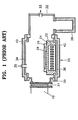
- a cassette chamber in which a carrier having a wafer is loaded, a reaction chamber in which a processing for fabricating a semiconductor device proceeds, and a wafer cooling chamber after completing the processing are respectively connected to a polyhedral transfer chamber having a robot arm for transferring the wafer to the respective chambers.
- the wafer for forming the polysilicon film is loaded in the cassette chamber 200.
- the robot arm 212 places the wafer on the susceptor 394 in the reaction chamber 220 through the wafer transfer chamber 210. Then, the temperature of the reaction chamber 220 is raised to a certain temperature by the heater 390 in the heating block 392.
Claims (10)
- Appareil de fabrication d'un dispositif semiconducteur comprenant :une chambre de cassette (200) pour loger une plaquette semi-conductrice ;une chambre de transfert de plaquette (210) ayant une partie avant raccordée à la chambre de cassette (200) ;une chambre de réaction (220) raccordée à une partie arrière de la chambre de transfert de plaquette (210) ; et une chambre de refroidissement de plaquette (230) raccordée à une partie latérale de la chambre de transfert de plaquette (210) ; caractérisé en ce que la chambre de réaction (220) a des première à quatrième chemises de refroidissement (400, 410, 420, 430) montées sur une première paroi de côté (300) adjacent à la chambre de transfert de plaquette (210), sur une seconde paroi de côté (320), opposée à la première paroi de côté (300), sur une paroi supérieure (340) et sur une paroi inférieure (360), respectivement.
- Appareil selon la revendication 1, comprenant en outre :un robinet-vanne (310) situé entre la chambre de réaction (220) et la chambre de transfert de plaquette (210) pour séparer la chambre de réaction (220) de la chambre de transfert de plaquette (210), le robinet-vanne (310) ayant une cinquième chemise de refroidissement (440).
- Appareil selon la revendication 2, dans lequel chacune des première (400), seconde (410), troisième (420) et cinquième (440) chemises de refroidissement a un réfrigérant choisi parmi le groupe qui se compose de l'eau de refroidissement et d'un mélange d'eau de refroidissement et du glycol d'éthylène.
- Procédé de fabrication d'un film de polysilicium dans l'appareil selon la revendication 1, comprenant les étapes consistant à :charger une plaquette pour former un film de polysilicium dans la chambre de cassette ;transférer la plaquette chargée à la chambre de réaction grâce à la chambre de transfert de plaquette ;faire circuler un réfrigérant dans la première jusqu'à la quatrième chemises de refroidissement ;former un film de silicium amorphe sur la plaquette en injectant dans la chambre de réaction un gaz choisi parmi le silane, le disilane et un mélange de gaz silane - disilane dans lequel le rapport silane : disilane varie entre un 30:1 et 1:30 ;transformer le film de silicium amorphe en un film de polysilicium sur lequel le HSG - Si est formé en traitant de manière thermique la plaquette ayant le film de silicium amorphe ; ettransférer la plaquette sur laquelle le HSG - Si est formé à la chambre de refroidissement et la refroidir.
- Procédé selon la revendication 4, dans lequel la température du réfrigérant est sensiblement inférieure à 9 °C.
- Procédé selon la revendication 4, dans lequel le film de polysilicium est une électrode inférieure d'un condensateur.
- Procédé selon la revendication 4, dans lequel la pression de la chambre de cassette est ajustée pour être inférieure à 6,67 x 10³ Pa (0,05 mtorr).
- Procédé selon la revendication 4 ou 6, dans lequel la pression de la chambre de cassette est ajustée en raréfiant pendant dix à trente minutes.
- Procédé selon la revendication 4, dans lequel la pression de la chambre de refroidissement et de la chambre de transfert de plaquette est ajustée pour être égale.
- Procédé selon la revendication 9, dans lequel la pression de la chambre de refroidissement et de la chambre de transfert de plaquette est ajustée pour être inférieure à 133 x 106 Pa (1,0 µtorr).
Priority Applications (3)
| Application Number | Priority Date | Filing Date | Title |
|---|---|---|---|
| DE69734877T DE69734877T2 (de) | 1997-09-10 | 1997-09-10 | Vorrichtung zur Herstellung von einem Halbleiter-Bauelement und ein diese Vorrichtung verwendendes Verfahren zur Herstellung einer Polysilicium-Schicht |
| EP97307010A EP0902459B1 (fr) | 1997-09-10 | 1997-09-10 | Un appareil pour la fabrication d'un dispositif semi-conducteur et une méthode pour la fabrication d'un film de poly-silicium utilisant un tel appareil |
| EP04076537A EP1455384A3 (fr) | 1997-09-10 | 1997-09-10 | Un appareil pour la fabrication d'un dispositif semi-conducteur et une méthode pour la fabrication d'un film de poly-silicium utilisant un tel appareil |
Applications Claiming Priority (1)
| Application Number | Priority Date | Filing Date | Title |
|---|---|---|---|
| EP97307010A EP0902459B1 (fr) | 1997-09-10 | 1997-09-10 | Un appareil pour la fabrication d'un dispositif semi-conducteur et une méthode pour la fabrication d'un film de poly-silicium utilisant un tel appareil |
Related Child Applications (1)
| Application Number | Title | Priority Date | Filing Date |
|---|---|---|---|
| EP04076537A Division EP1455384A3 (fr) | 1997-09-10 | 1997-09-10 | Un appareil pour la fabrication d'un dispositif semi-conducteur et une méthode pour la fabrication d'un film de poly-silicium utilisant un tel appareil |
Publications (2)
| Publication Number | Publication Date |
|---|---|
| EP0902459A1 EP0902459A1 (fr) | 1999-03-17 |
| EP0902459B1 true EP0902459B1 (fr) | 2005-12-14 |
Family
ID=8229504
Family Applications (2)
| Application Number | Title | Priority Date | Filing Date |
|---|---|---|---|
| EP97307010A Expired - Lifetime EP0902459B1 (fr) | 1997-09-10 | 1997-09-10 | Un appareil pour la fabrication d'un dispositif semi-conducteur et une méthode pour la fabrication d'un film de poly-silicium utilisant un tel appareil |
| EP04076537A Withdrawn EP1455384A3 (fr) | 1997-09-10 | 1997-09-10 | Un appareil pour la fabrication d'un dispositif semi-conducteur et une méthode pour la fabrication d'un film de poly-silicium utilisant un tel appareil |
Family Applications After (1)
| Application Number | Title | Priority Date | Filing Date |
|---|---|---|---|
| EP04076537A Withdrawn EP1455384A3 (fr) | 1997-09-10 | 1997-09-10 | Un appareil pour la fabrication d'un dispositif semi-conducteur et une méthode pour la fabrication d'un film de poly-silicium utilisant un tel appareil |
Country Status (2)
| Country | Link |
|---|---|
| EP (2) | EP0902459B1 (fr) |
| DE (1) | DE69734877T2 (fr) |
Family Cites Families (5)
| Publication number | Priority date | Publication date | Assignee | Title |
|---|---|---|---|---|
| US5254170A (en) * | 1989-08-07 | 1993-10-19 | Asm Vt, Inc. | Enhanced vertical thermal reactor system |
| US5516732A (en) * | 1992-12-04 | 1996-05-14 | Sony Corporation | Wafer processing machine vacuum front end method and apparatus |
| EP0608633B1 (fr) * | 1993-01-28 | 1999-03-03 | Applied Materials, Inc. | Procédé de dépÔt par CVD d'une structure multicouche dans une unique chambre de dépÔt |
| JP2833545B2 (ja) * | 1995-03-06 | 1998-12-09 | 日本電気株式会社 | 半導体装置の製造方法 |
| US5663090A (en) * | 1995-06-29 | 1997-09-02 | Micron Technology, Inc. | Method to thermally form hemispherical grain (HSG) silicon to enhance capacitance for application in high density DRAMs |
-
1997
- 1997-09-10 EP EP97307010A patent/EP0902459B1/fr not_active Expired - Lifetime
- 1997-09-10 EP EP04076537A patent/EP1455384A3/fr not_active Withdrawn
- 1997-09-10 DE DE69734877T patent/DE69734877T2/de not_active Expired - Fee Related
Also Published As
| Publication number | Publication date |
|---|---|
| EP1455384A2 (fr) | 2004-09-08 |
| DE69734877D1 (de) | 2006-01-19 |
| EP0902459A1 (fr) | 1999-03-17 |
| DE69734877T2 (de) | 2006-09-14 |
| EP1455384A3 (fr) | 2004-10-20 |
Similar Documents
| Publication | Publication Date | Title |
|---|---|---|
| US6039811A (en) | Apparatus for fabricating polysilicon film for semiconductor device | |
| JP3676983B2 (ja) | 半導体製造方法、基板処理方法、及び半導体製造装置 | |
| US5629043A (en) | Silicon nitride film formation method | |
| US4956204A (en) | Process of forming a film by low pressure chemical vapor deposition | |
| US4985372A (en) | Method of forming conductive layer including removal of native oxide | |
| JP2892170B2 (ja) | 熱処理成膜方法 | |
| KR19990045170A (ko) | 요철상 폴리실리콘층의 형성방법 및 이 방법의 실시에 사용되는기판처리장치와 반도체 메모리디바이스 | |
| JP3741518B2 (ja) | 半導体メモリ装置のキャパシタ下部電極の製造方法 | |
| US6350321B1 (en) | UHV horizontal hot wall cluster CVD/growth design | |
| JP5355514B2 (ja) | 半導体製造方法、基板処理方法および基板処理装置 | |
| EP0902459B1 (fr) | Un appareil pour la fabrication d'un dispositif semi-conducteur et une méthode pour la fabrication d'un film de poly-silicium utilisant un tel appareil | |
| JP4669257B2 (ja) | 半導体製造方法、基板処理方法、及び基板処理装置 | |
| KR100331964B1 (ko) | 원자층 증착 설비 및 이를 이용한 원자층 증착 방법 | |
| JP2000150815A (ja) | 半導体装置の製造方法及び半導体製造装置 | |
| EP0902462B1 (fr) | Procédé de fabrication d'une électrode inférieure pour un dispositif de mémoire à semiconducteurs | |
| JP4240941B2 (ja) | 半導体装置の製造方法および基板処理装置 | |
| KR19990013845A (ko) | 반도체 장치의 제조방법 | |
| US6194292B1 (en) | Method of fabricating in-situ doped rough polycrystalline silicon using a single wafer reactor | |
| JP4456341B2 (ja) | 半導体装置の製造方法および基板処理装置 | |
| US20010031556A1 (en) | System and method for integrated oxide removal and processing of a semiconductor wafer | |
| JP2002222871A (ja) | 熱処理方法 | |
| US6066538A (en) | Methods and apparatus for forming integrated circuit capacitors having composite oxide-nitride-oxide dielectric layers therein | |
| JP2000200883A (ja) | メモリセル用キャパシタの製作方法及び基板処理装置 | |
| KR100238205B1 (ko) | HSG-Si 이 표면에 형성되어 있는 다결정 실리콘막의 제조방법 | |
| KR20010018996A (ko) | 매엽식 반도체 제조장비의 웨이퍼 처리방법 |
Legal Events
| Date | Code | Title | Description |
|---|---|---|---|
| PUAI | Public reference made under article 153(3) epc to a published international application that has entered the european phase |
Free format text: ORIGINAL CODE: 0009012 |
|
| 17P | Request for examination filed |
Effective date: 19970917 |
|
| AK | Designated contracting states |
Kind code of ref document: A1 Designated state(s): DE FR GB NL |
|
| AX | Request for extension of the european patent |
Free format text: AL;LT;LV;RO;SI |
|
| AKX | Designation fees paid |
Free format text: DE FR GB NL |
|
| 17Q | First examination report despatched |
Effective date: 20031006 |
|
| GRAP | Despatch of communication of intention to grant a patent |
Free format text: ORIGINAL CODE: EPIDOSNIGR1 |
|
| GRAS | Grant fee paid |
Free format text: ORIGINAL CODE: EPIDOSNIGR3 |
|
| GRAA | (expected) grant |
Free format text: ORIGINAL CODE: 0009210 |
|
| AK | Designated contracting states |
Kind code of ref document: B1 Designated state(s): DE FR GB NL |
|
| REG | Reference to a national code |
Ref country code: GB Ref legal event code: FG4D |
|
| REF | Corresponds to: |
Ref document number: 69734877 Country of ref document: DE Date of ref document: 20060119 Kind code of ref document: P |
|
| PLBE | No opposition filed within time limit |
Free format text: ORIGINAL CODE: 0009261 |
|
| STAA | Information on the status of an ep patent application or granted ep patent |
Free format text: STATUS: NO OPPOSITION FILED WITHIN TIME LIMIT |
|
| 26N | No opposition filed |
Effective date: 20060915 |
|
| EN | Fr: translation not filed | ||
| ET | Fr: translation filed | ||
| REG | Reference to a national code |
Ref country code: FR Ref legal event code: EERR Free format text: CORRECTION DE BOPI 07/05 - BREVETS EUROPEENS DONT LA TRADUCTION N A PAS ETE REMISE A L INPI. IL Y A LIEU DE SUPPRIMER : LA MENTION DE LA NON REMISE. LA REMISE DE LA TRADUCTION EST PUBLIEE DANS LE PRESENT BOPI. |
|
| PGFP | Annual fee paid to national office [announced via postgrant information from national office to epo] |
Ref country code: NL Payment date: 20080903 Year of fee payment: 12 Ref country code: FR Payment date: 20080915 Year of fee payment: 12 |
|
| PGFP | Annual fee paid to national office [announced via postgrant information from national office to epo] |
Ref country code: GB Payment date: 20080910 Year of fee payment: 12 |
|
| PGFP | Annual fee paid to national office [announced via postgrant information from national office to epo] |
Ref country code: DE Payment date: 20080926 Year of fee payment: 12 |
|
| REG | Reference to a national code |
Ref country code: NL Ref legal event code: V1 Effective date: 20100401 |
|
| GBPC | Gb: european patent ceased through non-payment of renewal fee |
Effective date: 20090910 |
|
| REG | Reference to a national code |
Ref country code: FR Ref legal event code: ST Effective date: 20100531 |
|
| PG25 | Lapsed in a contracting state [announced via postgrant information from national office to epo] |
Ref country code: NL Free format text: LAPSE BECAUSE OF NON-PAYMENT OF DUE FEES Effective date: 20100401 Ref country code: FR Free format text: LAPSE BECAUSE OF NON-PAYMENT OF DUE FEES Effective date: 20090930 Ref country code: DE Free format text: LAPSE BECAUSE OF NON-PAYMENT OF DUE FEES Effective date: 20100401 |
|
| PG25 | Lapsed in a contracting state [announced via postgrant information from national office to epo] |
Ref country code: GB Free format text: LAPSE BECAUSE OF NON-PAYMENT OF DUE FEES Effective date: 20090910 |