EP0902461A3 - Process for forming structures with high aspect ratio - Google Patents
Process for forming structures with high aspect ratio Download PDFInfo
- Publication number
- EP0902461A3 EP0902461A3 EP98114572A EP98114572A EP0902461A3 EP 0902461 A3 EP0902461 A3 EP 0902461A3 EP 98114572 A EP98114572 A EP 98114572A EP 98114572 A EP98114572 A EP 98114572A EP 0902461 A3 EP0902461 A3 EP 0902461A3
- Authority
- EP
- European Patent Office
- Prior art keywords
- mask
- aspect ratio
- layer
- high aspect
- structures
- Prior art date
- Legal status (The legal status is an assumption and is not a legal conclusion. Google has not performed a legal analysis and makes no representation as to the accuracy of the status listed.)
- Withdrawn
Links
Classifications
-
- C—CHEMISTRY; METALLURGY
- C23—COATING METALLIC MATERIAL; COATING MATERIAL WITH METALLIC MATERIAL; CHEMICAL SURFACE TREATMENT; DIFFUSION TREATMENT OF METALLIC MATERIAL; COATING BY VACUUM EVAPORATION, BY SPUTTERING, BY ION IMPLANTATION OR BY CHEMICAL VAPOUR DEPOSITION, IN GENERAL; INHIBITING CORROSION OF METALLIC MATERIAL OR INCRUSTATION IN GENERAL
- C23F—NON-MECHANICAL REMOVAL OF METALLIC MATERIAL FROM SURFACE; INHIBITING CORROSION OF METALLIC MATERIAL OR INCRUSTATION IN GENERAL; MULTI-STEP PROCESSES FOR SURFACE TREATMENT OF METALLIC MATERIAL INVOLVING AT LEAST ONE PROCESS PROVIDED FOR IN CLASS C23 AND AT LEAST ONE PROCESS COVERED BY SUBCLASS C21D OR C22F OR CLASS C25
- C23F4/00—Processes for removing metallic material from surfaces, not provided for in group C23F1/00 or C23F3/00
-
- H—ELECTRICITY
- H10—SEMICONDUCTOR DEVICES; ELECTRIC SOLID-STATE DEVICES NOT OTHERWISE PROVIDED FOR
- H10B—ELECTRONIC MEMORY DEVICES
- H10B12/00—Dynamic random access memory [DRAM] devices
- H10B12/01—Manufacture or treatment
- H10B12/02—Manufacture or treatment for one transistor one-capacitor [1T-1C] memory cells
- H10B12/03—Making the capacitor or connections thereto
- H10B12/033—Making the capacitor or connections thereto the capacitor extending over the transistor
-
- H—ELECTRICITY
- H10—SEMICONDUCTOR DEVICES; ELECTRIC SOLID-STATE DEVICES NOT OTHERWISE PROVIDED FOR
- H10D—INORGANIC ELECTRIC SEMICONDUCTOR DEVICES
- H10D1/00—Resistors, capacitors or inductors
- H10D1/01—Manufacture or treatment
- H10D1/041—Manufacture or treatment of capacitors having no potential barriers
- H10D1/042—Manufacture or treatment of capacitors having no potential barriers using deposition processes to form electrode extensions
-
- H—ELECTRICITY
- H10—SEMICONDUCTOR DEVICES; ELECTRIC SOLID-STATE DEVICES NOT OTHERWISE PROVIDED FOR
- H10D—INORGANIC ELECTRIC SEMICONDUCTOR DEVICES
- H10D1/00—Resistors, capacitors or inductors
- H10D1/60—Capacitors
- H10D1/68—Capacitors having no potential barriers
- H10D1/682—Capacitors having no potential barriers having dielectrics comprising perovskite structures
-
- H—ELECTRICITY
- H10—SEMICONDUCTOR DEVICES; ELECTRIC SOLID-STATE DEVICES NOT OTHERWISE PROVIDED FOR
- H10D—INORGANIC ELECTRIC SEMICONDUCTOR DEVICES
- H10D1/00—Resistors, capacitors or inductors
- H10D1/60—Capacitors
- H10D1/68—Capacitors having no potential barriers
- H10D1/692—Electrodes
- H10D1/711—Electrodes having non-planar surfaces, e.g. formed by texturisation
- H10D1/716—Electrodes having non-planar surfaces, e.g. formed by texturisation having vertical extensions
-
- H—ELECTRICITY
- H10—SEMICONDUCTOR DEVICES; ELECTRIC SOLID-STATE DEVICES NOT OTHERWISE PROVIDED FOR
- H10P—GENERIC PROCESSES OR APPARATUS FOR THE MANUFACTURE OR TREATMENT OF DEVICES COVERED BY CLASS H10
- H10P14/00—Formation of materials, e.g. in the shape of layers or pillars
- H10P14/60—Formation of materials, e.g. in the shape of layers or pillars of insulating materials
- H10P14/69—Inorganic materials
- H10P14/692—Inorganic materials composed of oxides, glassy oxides or oxide-based glasses
- H10P14/6938—Inorganic materials composed of oxides, glassy oxides or oxide-based glasses the material containing at least one metal element, e.g. metal oxides, metal oxynitrides or metal oxycarbides
- H10P14/69398—Inorganic materials composed of oxides, glassy oxides or oxide-based glasses the material containing at least one metal element, e.g. metal oxides, metal oxynitrides or metal oxycarbides the material having a perovskite structure, e.g. BaTiO3
-
- H—ELECTRICITY
- H10—SEMICONDUCTOR DEVICES; ELECTRIC SOLID-STATE DEVICES NOT OTHERWISE PROVIDED FOR
- H10P—GENERIC PROCESSES OR APPARATUS FOR THE MANUFACTURE OR TREATMENT OF DEVICES COVERED BY CLASS H10
- H10P50/00—Etching of wafers, substrates or parts of devices
- H10P50/71—Etching of wafers, substrates or parts of devices using masks for conductive or resistive materials
-
- H—ELECTRICITY
- H10—SEMICONDUCTOR DEVICES; ELECTRIC SOLID-STATE DEVICES NOT OTHERWISE PROVIDED FOR
- H10P—GENERIC PROCESSES OR APPARATUS FOR THE MANUFACTURE OR TREATMENT OF DEVICES COVERED BY CLASS H10
- H10P76/00—Manufacture or treatment of masks on semiconductor bodies, e.g. by lithography or photolithography
- H10P76/40—Manufacture or treatment of masks on semiconductor bodies, e.g. by lithography or photolithography of masks comprising inorganic materials
- H10P76/408—Manufacture or treatment of masks on semiconductor bodies, e.g. by lithography or photolithography of masks comprising inorganic materials characterised by their sizes, orientations, dispositions, behaviours or shapes
- H10P76/4083—Manufacture or treatment of masks on semiconductor bodies, e.g. by lithography or photolithography of masks comprising inorganic materials characterised by their sizes, orientations, dispositions, behaviours or shapes characterised by their behaviours during the lithography processes, e.g. soluble masks or redeposited masks
Landscapes
- Engineering & Computer Science (AREA)
- Chemical & Material Sciences (AREA)
- Manufacturing & Machinery (AREA)
- Materials Engineering (AREA)
- Mechanical Engineering (AREA)
- Metallurgy (AREA)
- Organic Chemistry (AREA)
- Semiconductor Memories (AREA)
- Drying Of Semiconductors (AREA)
- Shielding Devices Or Components To Electric Or Magnetic Fields (AREA)
- Manufacturing Of Electric Cables (AREA)
Abstract
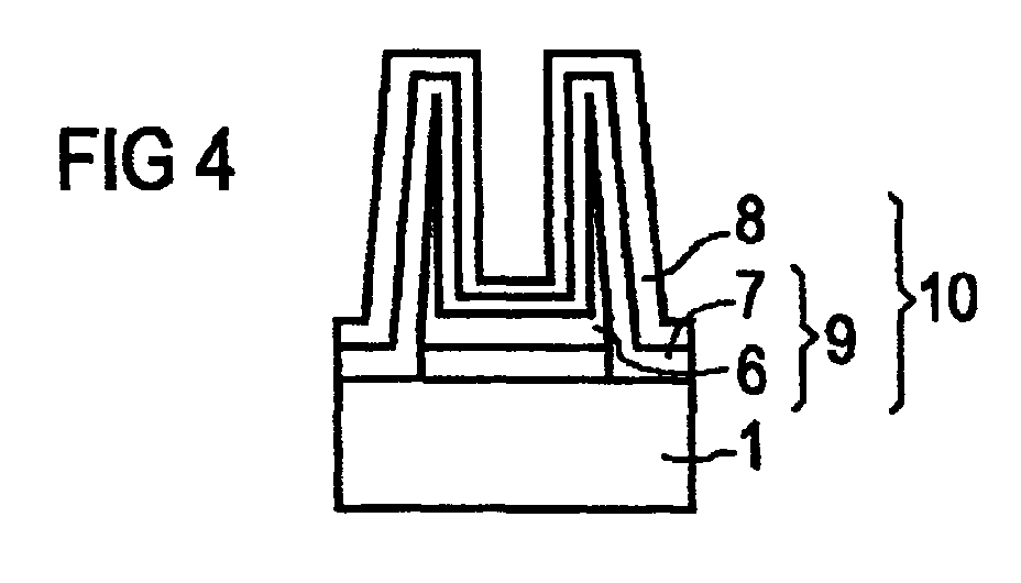
Erfindungsgemäß wird ein zur Erzeugung von Strukturen mit einem hohen Aspektverhältnis bereitgestellt, das die folgenden Schritte aufweist: das Material der zu erzeugenden Struktur wird in Form einer Schicht bereitgestellt, auf die Schicht wird eine Maske aufgebracht, die Schicht wird unter Verwendung der Maske trockengeätzt, so daß Redepositionen des Schichtmaterials an den Seitenwänden der Maske gebildet werden, die Maske wird entfernt, so daß eine Struktur mit einem hohen Aspektverhältnis zurückbleibt.According to the invention, one is used to generate structures with a high aspect ratio provided the following Steps comprises: the material of the structure to be created is provided in the form of a layer, on top of the layer a mask is applied, the layer is used the mask is etched dry, so that the speeches of the Layer material are formed on the side walls of the mask, the mask is removed so that a structure with a remains high aspect ratio.
Durch das erfindungsgemäße Verfahren lassen sich sehr hohe (≥
1 µm) und sehr dünne (≤ 50 nm) Strukturen in nur sehr wenigen
Prozeßschritten und mit nur einer Maskentechnik relativ einfach
und schnell erzeugen. Strukturen mit so großen Aspektverhältnissen,
insbesondere wenn sie aus einem leitenden Material
bestehen, können anders nicht oder nur mit hohem Aufwand
erzeugt werden.
Applications Claiming Priority (2)
| Application Number | Priority Date | Filing Date | Title |
|---|---|---|---|
| DE19739224 | 1997-09-08 | ||
| DE19739224 | 1997-09-08 |
Publications (2)
| Publication Number | Publication Date |
|---|---|
| EP0902461A2 EP0902461A2 (en) | 1999-03-17 |
| EP0902461A3 true EP0902461A3 (en) | 2000-10-11 |
Family
ID=7841545
Family Applications (1)
| Application Number | Title | Priority Date | Filing Date |
|---|---|---|---|
| EP98114572A Withdrawn EP0902461A3 (en) | 1997-09-08 | 1998-07-31 | Process for forming structures with high aspect ratio |
Country Status (6)
| Country | Link |
|---|---|
| US (1) | US6210595B1 (en) |
| EP (1) | EP0902461A3 (en) |
| JP (1) | JPH11154668A (en) |
| KR (1) | KR19990029609A (en) |
| CN (1) | CN1211067A (en) |
| TW (1) | TW430900B (en) |
Families Citing this family (10)
| Publication number | Priority date | Publication date | Assignee | Title |
|---|---|---|---|---|
| TW430900B (en) * | 1997-09-08 | 2001-04-21 | Siemens Ag | Method for producing structures having a high aspect ratio |
| SG79292A1 (en) * | 1998-12-11 | 2001-03-20 | Hitachi Ltd | Semiconductor integrated circuit and its manufacturing method |
| US6782610B1 (en) * | 1999-05-21 | 2004-08-31 | North Corporation | Method for fabricating a wiring substrate by electroplating a wiring film on a metal base |
| DE10147929C1 (en) * | 2001-09-28 | 2003-04-17 | Infineon Technologies Ag | Method of manufacturing a semiconductor structure and use of the method |
| US7064078B2 (en) * | 2004-01-30 | 2006-06-20 | Applied Materials | Techniques for the use of amorphous carbon (APF) for various etch and litho integration scheme |
| KR100645041B1 (en) * | 2004-07-12 | 2006-11-10 | 삼성전자주식회사 | Semiconductor device having MM capacitor and method for forming same |
| DE102005039667A1 (en) * | 2005-08-22 | 2007-03-01 | Infineon Technologies Ag | Producing a low aspect ratio structure and buried strap for a trench DRAM forms and fills trench in semiconductor substrate with initial and sacrificial layers and selectively removes especially at sidewalls |
| US9871044B2 (en) * | 2015-11-06 | 2018-01-16 | Micron Technology, Inc. | Enhanced charge storage materials, related semiconductor memory cells and semiconductor devices, and related systems and methods |
| US10562763B2 (en) * | 2017-08-28 | 2020-02-18 | Taiwan Semiconductor Manufacturing Co., Ltd. | Fence structure to prevent stiction in a MEMS motion sensor |
| EP3637448A4 (en) * | 2018-08-21 | 2020-10-07 | Shenzhen Weitongbo Technology Co., Ltd. | CAPACITOR AND MANUFACTURING METHOD FOR IT |
Citations (3)
| Publication number | Priority date | Publication date | Assignee | Title |
|---|---|---|---|---|
| JPS63211740A (en) * | 1987-02-27 | 1988-09-02 | Oki Electric Ind Co Ltd | Method for forming wiring pattern of semiconductor element |
| WO1996027208A1 (en) * | 1995-02-28 | 1996-09-06 | Micron Technology, Inc. | Method for forming a structure using redeposition |
| JPH1041478A (en) * | 1996-04-23 | 1998-02-13 | Internatl Business Mach Corp <Ibm> | Method for producing electric device and composite stack electrode |
Family Cites Families (13)
| Publication number | Priority date | Publication date | Assignee | Title |
|---|---|---|---|---|
| US4400257A (en) | 1982-12-21 | 1983-08-23 | Rca Corporation | Method of forming metal lines |
| US4533430A (en) * | 1984-01-04 | 1985-08-06 | Advanced Micro Devices, Inc. | Process for forming slots having near vertical sidewalls at their upper extremities |
| US4702795A (en) | 1985-05-03 | 1987-10-27 | Texas Instruments Incorporated | Trench etch process |
| JPH0622218B2 (en) * | 1988-08-06 | 1994-03-23 | 富士通株式会社 | Etching method |
| CA2061119C (en) * | 1991-04-19 | 1998-02-03 | Pei-Ing P. Lee | Method of depositing conductors in high aspect ratio apertures |
| JPH0613357A (en) * | 1992-06-25 | 1994-01-21 | Seiko Epson Corp | Method for etching semiconductor device |
| US5468340A (en) * | 1992-10-09 | 1995-11-21 | Gupta; Subhash | Highly selective high aspect ratio oxide etch method and products made by the process |
| US5258093A (en) * | 1992-12-21 | 1993-11-02 | Motorola, Inc. | Procss for fabricating a ferroelectric capacitor in a semiconductor device |
| US5409563A (en) * | 1993-02-26 | 1995-04-25 | Micron Technology, Inc. | Method for etching high aspect ratio features |
| JPH07130702A (en) * | 1993-11-08 | 1995-05-19 | Fujitsu Ltd | Method for patterning metal film made of platinum or palladium |
| KR970054009A (en) * | 1995-12-16 | 1997-07-31 | 김주용 | Capacitor Manufacturing Method of Semiconductor Device |
| US5728619A (en) * | 1996-03-20 | 1998-03-17 | Taiwan Semiconductor Manufacturing Company, Ltd. | Selective reactive Ion etch (RIE) method for forming a narrow line-width high aspect ratio via through an integrated circuit layer |
| TW430900B (en) * | 1997-09-08 | 2001-04-21 | Siemens Ag | Method for producing structures having a high aspect ratio |
-
1998
- 1998-07-06 TW TW087110890A patent/TW430900B/en not_active IP Right Cessation
- 1998-07-31 EP EP98114572A patent/EP0902461A3/en not_active Withdrawn
- 1998-08-07 CN CN98118878A patent/CN1211067A/en active Pending
- 1998-09-03 JP JP10249255A patent/JPH11154668A/en not_active Abandoned
- 1998-09-08 KR KR1019980036881A patent/KR19990029609A/en not_active Ceased
- 1998-09-08 US US09/149,829 patent/US6210595B1/en not_active Expired - Lifetime
Patent Citations (4)
| Publication number | Priority date | Publication date | Assignee | Title |
|---|---|---|---|---|
| JPS63211740A (en) * | 1987-02-27 | 1988-09-02 | Oki Electric Ind Co Ltd | Method for forming wiring pattern of semiconductor element |
| WO1996027208A1 (en) * | 1995-02-28 | 1996-09-06 | Micron Technology, Inc. | Method for forming a structure using redeposition |
| JPH1041478A (en) * | 1996-04-23 | 1998-02-13 | Internatl Business Mach Corp <Ibm> | Method for producing electric device and composite stack electrode |
| US5825609A (en) * | 1996-04-23 | 1998-10-20 | International Business Machines Corporation | Compound electrode stack capacitor |
Non-Patent Citations (1)
| Title |
|---|
| PATENT ABSTRACTS OF JAPAN vol. 012, no. 500 (E - 699) 27 December 1988 (1988-12-27) * |
Also Published As
| Publication number | Publication date |
|---|---|
| KR19990029609A (en) | 1999-04-26 |
| JPH11154668A (en) | 1999-06-08 |
| US6210595B1 (en) | 2001-04-03 |
| EP0902461A2 (en) | 1999-03-17 |
| TW430900B (en) | 2001-04-21 |
| CN1211067A (en) | 1999-03-17 |
Similar Documents
| Publication | Publication Date | Title |
|---|---|---|
| DE10205764B4 (en) | Improved method of fabricating a thin film bulk acoustic resonator (FBAR) and FBAR structure incorporating this method | |
| EP0973050A3 (en) | Method for manufacturing planar waveguide structures and waveguide structure | |
| EP0627764A2 (en) | Process for the separation of chips on a wafer | |
| EP1810947A3 (en) | Semiconductor device and its process of fabrication | |
| DE19713014A1 (en) | Quartz glass component for use in semiconductor manufacturing | |
| DE19719601A1 (en) | Acceleration sensor with spring-mounted seismic mass | |
| DE69329369T2 (en) | Process for etching a silicon substrate | |
| DE99958136T1 (en) | QUARTZ GLASS HOLDING DEVICE WITH LARGE SURFACE IRREGULARITIES AND METHOD FOR THE PRODUCTION THEREOF | |
| DE1954499A1 (en) | Process for the production of semiconductor circuits with interconnects | |
| DE69313648T2 (en) | GASKET PRODUCTION | |
| EP0889506A3 (en) | Etching process | |
| DE19824401B4 (en) | Process for the preparation of a sensor membrane substrate | |
| EP0907203A3 (en) | Patterning method | |
| DE4232821A1 (en) | FINE-STRUCTURED SEMICONDUCTOR COMPONENT AND METHOD FOR THE PRODUCTION THEREOF | |
| EP0711420A1 (en) | Process of manufacturing a silicon semiconductor substrate with an integrated waveguide coupled to an optical fibre | |
| WO1999017349A1 (en) | Method for producing an open three-dimensional microstructure | |
| EP1360143B1 (en) | Method for producing surface micromechanical structures, and sensor | |
| DE4446852A1 (en) | Forming microstructure for semiconductor device | |
| DE3232837A1 (en) | METHOD FOR PRODUCING A 2-LEVEL METALIZATION FOR SEMICONDUCTOR COMPONENTS, IN PARTICULAR FOR PERFORMANCE SEMICONDUCTOR COMPONENTS LIKE THYRISTORS | |
| DE19945170B4 (en) | Method for producing a stencil mask | |
| EP0957509A3 (en) | Process for the fabrication of a device containing a microstructured layer | |
| EP1164631A3 (en) | Process for forming openings in a layer | |
| DE3927163A1 (en) | METHOD FOR STRUCTURING A SEMICONDUCTOR BODY | |
| WO2000022657A1 (en) | Method for micro-structuring glasses | |
| EP0794564A3 (en) | Process for fabricating discrete electronic elements |
Legal Events
| Date | Code | Title | Description |
|---|---|---|---|
| PUAI | Public reference made under article 153(3) epc to a published international application that has entered the european phase |
Free format text: ORIGINAL CODE: 0009012 |
|
| AK | Designated contracting states |
Kind code of ref document: A2 Designated state(s): DE FR GB IE IT |
|
| AX | Request for extension of the european patent |
Free format text: AL;LT;LV;MK;RO;SI |
|
| PUAL | Search report despatched |
Free format text: ORIGINAL CODE: 0009013 |
|
| AK | Designated contracting states |
Kind code of ref document: A3 Designated state(s): AT BE CH CY DE DK ES FI FR GB GR IE IT LI LU MC NL PT SE |
|
| AX | Request for extension of the european patent |
Free format text: AL;LT;LV;MK;RO;SI |
|
| RIC1 | Information provided on ipc code assigned before grant |
Free format text: 7H 01L 21/3213 A |
|
| 17P | Request for examination filed |
Effective date: 20001106 |
|
| AKX | Designation fees paid |
Free format text: DE FR GB IE IT |
|
| RAP1 | Party data changed (applicant data changed or rights of an application transferred) |
Owner name: INFINEON TECHNOLOGIES AG |
|
| STAA | Information on the status of an ep patent application or granted ep patent |
Free format text: STATUS: THE APPLICATION IS DEEMED TO BE WITHDRAWN |
|
| 18D | Application deemed to be withdrawn |
Effective date: 20060420 |