EP0902486A2 - Lichtemittierendes Halbleiterbauelement und Verfahren zu dessen Herstellung - Google Patents
Lichtemittierendes Halbleiterbauelement und Verfahren zu dessen Herstellung Download PDFInfo
- Publication number
- EP0902486A2 EP0902486A2 EP98117179A EP98117179A EP0902486A2 EP 0902486 A2 EP0902486 A2 EP 0902486A2 EP 98117179 A EP98117179 A EP 98117179A EP 98117179 A EP98117179 A EP 98117179A EP 0902486 A2 EP0902486 A2 EP 0902486A2
- Authority
- EP
- European Patent Office
- Prior art keywords
- conductivity type
- silicon layer
- layer
- nanostructure
- type
- Prior art date
- Legal status (The legal status is an assumption and is not a legal conclusion. Google has not performed a legal analysis and makes no representation as to the accuracy of the status listed.)
- Granted
Links
Images


Classifications
-
- H—ELECTRICITY
- H10—SEMICONDUCTOR DEVICES; ELECTRIC SOLID-STATE DEVICES NOT OTHERWISE PROVIDED FOR
- H10H—INORGANIC LIGHT-EMITTING SEMICONDUCTOR DEVICES HAVING POTENTIAL BARRIERS
- H10H20/00—Individual inorganic light-emitting semiconductor devices having potential barriers, e.g. light-emitting diodes [LED]
- H10H20/80—Constructional details
- H10H20/81—Bodies
- H10H20/822—Materials of the light-emitting regions
- H10H20/826—Materials of the light-emitting regions comprising only Group IV materials
- H10H20/8264—Materials of the light-emitting regions comprising only Group IV materials comprising polycrystalline, amorphous or porous Group IV materials
Definitions
- the present invention relates to a semiconductor light emitting device used in an optoelectronic integrated circuit and an image display device, and more particularly to a semiconductor light emitting device and a method for manufacturing the same using a porous silicon.
- the porous silicon differs from a crystalline silicon (hereinafter referred to as a "c-Si") in optical properties, and absorption edge energy generally becomes large. Moreover, electrical properties also changes, and the resistivity becomes high as compared with the original c-Si.
- PSs Three kinds of PSs are known as follows:
- the PS of which a porosity is 20 to 80 % and the diameter of microporous holes is not more than approximate 2 nm is referred to as "a nanostructure PS".
- the nanostructure PS Differing from the c-Si, the nanostructure PS shows luminescence in a visible-light range. Pumping this nanostructure PS by the shorter wavelength light within the spectral region from blue to ultra violet, photoluminescence (PL) of a luminescence efficiency (external quantum efficiency) of approximate 10 % at the maximum can be observed. Moreover, electroluminescence (EL) can be obtained also by injecting current into the nanostructure PS.
- PL photoluminescence
- EL electroluminescence
- the PS of which the porosity is 40 to 60 % and the diameter of the microporous holes is approximate 2 to 50 nm is referred to as "a mesostructure PS".
- the luminescence efficiency of the mesostructure PS is generally low as compared with the nanostructure PS, and an emission wavelength also generally comes to the longer wavelength than the nanostructure PS.
- the mesostructure PS is coarse in structure as compared with the nanostructure PS and is low in resistivity as compared with the nanostructure PS.
- a PS of which the porosity is further low than the mesostructure PS and the diameter of the microporous holes is 50 nm or more is referred to as "a microstructure PS".
- the macrostructure PS can hardly emit light and is further low in resistivity as compared with the mesostructure PS.
- PSs are formed by anodization, or by feeding a current inwardly from the surface of the silicon through the c-Si (single crystal silicon or polycrystalline silicon) as electrodes in the solution containing hydrogen fluoride (HF).
- HF hydrogen fluoride
- materials such as platinum (Pt) being usually not dissolved into an anodization solution is used.
- the PS and the material having the structure similar thereto can be made by other methods, they are omitted because of being not important in the invention.
- the PS is constituted by the number of the microporous holes of the diameter of approximate 1 to 100 nm, remained small c-Si particles or a skeleton, and an amorphous portion surrounding thereabouts.
- the structure of the PS being made is changed, whereby the nanostructure PS, the mesostructure PS or the macrostructure PS can be obtained.
- the nanostructure PS is obtained by anodizing the c-Si containing a p-type impurity doped to the extent being not degenerated (a non-degenerate p-type). Moreover, the nanostructure PS is obtained also by anodization while irradiating a non-degenerate n-type c-Si of a low impurity concentration with light.
- This nanostructure PS is fine so that the porosity is approximate 20 to 80 % and the diameter of the holes is not more than 2 nm. That is, since remaining c-Si particles or a size of the skeleton are fine, the resistivity becomes high as compared with that of the original c-Si.
- the nanostructure PS can be obtained by anodizing the degenerate p-type c-Si or the degenerate n-type c-Si, containing the p-type or n-type impurity with higher impurity concentration so that the Fermi level is located within the valence or conduction band.
- the macrostructure PS can be obtained by anodizing the non-degenerate n-type c-Si in a darkroom.
- the above-noted description of the three kinds of PSs which differ in structure is performed on the generalized characteristics of the respectively typical one, and actually, there are the PSs having the characteristic intermediate between the mesostructure PS and the nanostructure PS and the PSs having the characteristic intermediate between the mesostructure PS and the macrostructure PS or the like.
- the PS belonging to the same nanostructure PS can differ in the fine structure in some cases depending upon the difference of a conductivity type of the original c-Si.
- the PS of which the structure differs in the direction of a depth can be made depending upon anodizing conditions.
- the PS belonging to the mesostructure PS or the macrostructure PS as the general structure and characteristic the PS containing the nanostructure PS can be made partially in the microscopic portion depending upon the anodizing conditions.
- This PS light emitting device is made by preparing a c-Si wafer that the p + type c-Si layer is formed on the n-type c-Si substrate to anodize the surface of this c-Si wafer under the irradiating with light using a lamp.
- the p + type c-Si layer of the surface of which resistivity is low becomes the mesostructure PS layer and the n-type c-Si substrate portion of the area which no light from the lamp reaches becomes the macrostructure PS.
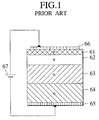
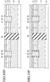
- Fig. 1 and Fig. 2 the structure and the equipment for manufacturing this PS light emitting device are shown.
- the macrostructure PS layer 63 made from the n-type c-Si is formed on a n-type c-Si substrate 64.
- the nanostructure PS layer 62 made from the n-type c-Si is formed on the n-type macrostructure PS layer 63.
- the mesostructure PS layer 61 made from the p + type c-Si is formed thereon.
- the expressions of "the n-type macrostructure PS layer”, “the n-type nanostructure PS layer”, “the p-type mesostructure PS layer” or the like are expressed for convenience and differ from the n-type and the p-type in the c-Si. The reason why is that, generally, in the PS layer, acceptor impurities and donor impurities are inactivated at room temperature.
- a translucent gold electrode 66 which selves as an anode is formed on the p-type mesostructure PS layer 61 and an aluminum electrode 65 which serves as a cathode is formed on the back of the n-type c-Si substrate 64.
- a direct current power supply 67 for the EL is connected between the anode 66 and the cathode 65.
- the n-type nanostructure PS layer 62 acts as an EL actve layer.
- the p-type mesostructure PS layer 61 has a function to form a junction similar to the pn-junction in the c-Si (hereinafter, such kind of junction by the PS layer is referred to as a "the pn-junction" for convenience) between the n-type nanostructure PS layer 62 and the p-type mesostructure PS layer 61, and a function to get better ohmic contact with the translucent gold electrode 66 formed on the layer 61.
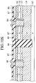
- a c-Si wafer 7 on which a p + type c-Si layer 71 of 0.6 ⁇ m in thickness and resistivity of 2x10 -3 ⁇ -cm is formed on a surface of a n-type c-Si substrate 72 of 500 ⁇ m and resistivity of 5 ⁇ -cm using a thermal diffusion method is prepared.
- it can be manufactured by anodizing this c-Si wafer 7 as shown in Fig. 2. That is, as shown in Fig.
- a container 1 for anodization which is made of polytetrafluoroethylene(PTFE), having an opening on the bottom is contacted closely with the surface of the p + type c-Si layer 71 using O-rings 2 to fill an anodizing mixed solution consisting of hydrofluoric acid and ethyl alcohol 4 into this container made of PTFE 1. Because of using the O-ring 2, the anodizing mixed solution consisting of hydrofluoric acid and ethyl alcohol 4 does not leak from the bottom of the container 1 made of PTFE.
- the anodization solution 4 consists of hydrofluoric acid of 50 weight percent and ethyl alcohol of 99.9 weight percent mixed at a volume ratio of 1: 1.
- a platinum electrode 3 is arranged in the anodizing mixed solution consisting of hydrofluoric acid and ethyl alcohol 4.
- the aluminum electrode 65 which will become the cathode shown in Fig. 1 eventually, and a desired anodizing current is fed through the anodizing mixed solution consisting of hydrofluoric acid and ethyl alcohol 4 by the variable direct current power supply 6 connected between the platinum electrode 3 and the aluminum electrode 65.
- the anodizing is performed while irradiating the p + type c-Si layer 71 and the n-type c-Si substrate 72 thereunder by a tungsten lamp 5 arranged on the upper of the container made of PTFE 1. Therefore, the platinum electrode 3 is arranged such that the light radiated from the tungsten lamp 5 can not be impeded to reach the surface of the c-Si wafer 7.
- the mesostructure PS layer 61 is obtained by anodizing the p + type c-Si layer 71 shown in Fig. 1. Moreover, the nanostructure PS layer 62 shown in Fig. 1 is formed at the portion in proximity to the surface influenced by light radiation in the n-type c-Si substrate 72 shown in Fig. 2. Moreover, the macrostructure PS layer 63 is formed at a slightly inner portion from the surface not influenced by light radiation in the n-type c-Si substrate 72. The n-type c-Si substrate 64 shown in Fig. 1 is a portion remaining as the c-Si of the n-type c-Si substrate 72 shown in Fig. 2. According to the method shown in Fig.
- the anode 66 shown in Fig. 1 is the translucent gold electrode formed by evaporating a gold thin film by a vacuum evaporation method after anodizing.
- the luminescence efficiency depends upon a way of anodizing and the anodization time, thereby not always being constant.
- the nanostructure PS layer anodized sufficiently by extending the anodization time has higher luminescence efficiency than that of the nanostructure PS layer anodized insufficiently with the shorter anodization time.
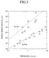
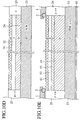
- Fig.3 shows a relationship between a series resistance Rs of such PS light emitting device and a thickness "d" of the nanostructure PS layer 62.
- a symbol of ⁇ shows the series resistance Rs of the light emitting device having the n-type nanostructure PS layer 62 shown in Fig.1.
- a symbol of ⁇ shows the series resistance Rs of the light emitting device, in which a luminescence layer is constituted by the p-type nanostructure PS layer made from the p-type c-Si, having the approximately same element structure as that shown by the symbol of ⁇ . It is understood that there is a relationship of approximately Rs ⁇ d 2 ⁇ 3 .
- the series resistance thereof becomes high inevitably.
- the series resistance Rs of the PS light emitting device whose external quantum efficiency is high as 0.1 to 1 %, becomes high as 100 k ⁇ to 1M ⁇ , and a high supply voltage is required in order to inject a current into such PS light emitting device. That is, electric energy converted to thermal energy is more increased with respect to electric energy converted to light energy, whereby the electric power efficiency would be decreased.
- the present invention is devised for solving the problems of the prior art described above, and the object of the invention is to reduce a series resistance Rs of a PS light emitting device to improve an electric power efficiency without impairing external quantum efficiency.
- the further object of the invention is to provide a light emitting device of which an operation voltage is low and an external quantum efficiency is high.
- the another object of the invention is to provide a method for manufacturing a PS light emitting device of which control of a film thickness of the luminescence layer is easy and the external quantum efficiency and an electric power efficiency are high.
- the additional object of the invention is to provide a method for manufacturing the PS light emitting device which can be integrated readily on the same silicon substrate with other electronic devices and can be manufactured inexpensively.
- a first feature of the invention is a semiconductor light emitting device at least comprising a first one conductivity type nanostructure porous silicon (PS) layer, an opposite conductivity type mesostructure PS layer disposed on the first one conductivity type nanostructure porous silicon (PS) layer, and a first one conductivity type mesostructure PS layer formed under the first one conductivity type nanostructure PS layer.
- the one conductivity type nanostructure PS layer is an abbreviated expression of the nanostructure PS layer formed from the one conductivity type crystalline silicon (c-Si)
- the opposite conductivity type mesostructure PS layer is an abbreviated expression of the mesostructure PS layer formed from the opposite conductivity type c-Si.
- the one conductivity type is n-type
- the opposite conductivity type is p-type
- the opposite conductivity type is n-type
- the one conductivity type mesostructure PS layer is an abbreviated expression of the mesostructure PS layer formed from the one conductivity type c-Si.
- the one conductivity type nanostructure PS layer is the layer which functions as the main light emitting layer, the resistivity is high. On the other hand, the luminescence efficiency and the resistivity of the first one conductivity type mesostructure PS layer are low.
- the nanostructure PS layer implies the PS layer of which the porosity is 20 to 80 % and the diameter of microporous holes is not more than approximate 2 nm as described above.
- the mesostructure PS layer implies the PS layer of which the porosity is 40 to 60 % and the diameter of microporous holes is not more than approximate 2 to 60 nm as described above.
- the pn-junction is formed between the first one conductivity type nanostructure PS layer and the opposite conductivity type mesostructure PS layer, and carriers are injected from the opposite conductivity type mesostructure PS layer to the first one conductivity type nanostructure PS layer, thereby light being emitted.
- the first one conductivity type nanostructure PS layer according to the invention may be formed by anodizing the non-degenerate crystalline silicon (c-Si) layer whose impurity concentration is low. That is, when anodizing the structure that the one conductivity type non-degenerate c-Si layer is sandwiched between the opposite conductivity type degenerate c-Si layer whose impurity concentration is high and the first one conductivity type degenerate c-Si layer, only the one conductivity type degenerate c-Si layer becomes the nanostructure PS layer, whereby a thickness can be controlled correctly.
- c-Si non-degenerate crystalline silicon
- the thickness of the first one conductivity type nanostructure PS layer which serves as the light emitting layer can be controlled into the predetermined thickness that the series resistance Rs is not increased and the maximum luminescence efficiency can be obtained.
- the thickness of the eventual first one conductivity type nanostructure PS layer is limited within the predetermined thickness, whereby, at anodizing, the sufficient anodization time can be expended to anodize sufficiently. That is to say, the nanostructure PS layer in the first feature of the invention is in the state that "transformation of crystalline silicon to porous silicon" has promoted sufficiently, and so to speak, the layer is the completed nanostructure PS layer. Therefore, according to the first feature of the invention, the light emission from this completed nanostructure PS layer is utilized, whereby the luminescence efficiency (the quantum efficiency) is extremely high as compared with the uncompleted nanostructure PS layer in the prior art.
- the first feature of the invention it is preferable to further comprise at least a second one conductivity type nanostructure PS layer and a second one conductivity type mesostructure PS layer under this second one conductivity type nanostructure PS layer on the lower of the first one conductivity type mesostructure PS layer.
- the second one conductivity type is the same conductivity type as the first one conductivity type.
- the second one conductivity type nanostructure PS layer also is the completed nanostructure PS layer.
- the series resistance Rs of the nanostructure PS layer is proportional to the square or the cube of the thickness "d" of the nanostructure PS layer, the series resistance becomes low suddenly when thinning the thickness of the nanostructure PS layer. Therefore, when connecting a plurality of thin nanostructure PS layers (N layers, defining N as a positive integer) in series, the total series resistance Rs (the total) becomes small value.
- the n-type nanostructure PS layers having the thickness of a fraction of N of the nanostructure PS layer of a single layer are prepared by N layers to form a stacked structure that the n-type mesostructure PS layers of N-1 layers are sandwiched between these N layers.
- the resistivity of the mesostructure PS layer is extremely low as compared with that of the nanostructure PS layer, it hardly contributes to the series resistance. Therefore, the total series resistance Rs (total) of this stacked structure is reduced to a fraction of N as compared with that of the single layer of the n-type nanostructure PS.
- a second feature of the invention relates to a method for manufacturing the semiconductor light emitting device according to the described-above first feature. That is, the second feature of the invention is a method for manufacturing the semiconductor light emitting device comprising the steps of : at least preparing a c-Si wafer comprising : at least the first one conductivity type degenerate crystalline silicon (c-Si) layer ; the first one conductivity type non-degenerate c-Si layer formed on the first one conductivity type degenerate c-Si layer ; and the opposite conductivity type degenerate c-Si layer formed on the first one conductivity type non-degenerate c-Si layer, and anodizing this c-Si wafer to transform the first one conductivity type non-degenerate c-Si layer to the first one conductivity type nanostructure PS layer.
- c-Si crystalline silicon
- the first one conductivity type degenerate c-Si layer and the opposite conductivity type degenerate c-Si layer are the c-Si layers whose impurity concentration are high and are transformed to the mesostructure PS layers respectively by anodization. Since the thickness of the first one conductivity type non-degenerate c-Si layer, whose impurity concentration is low, is defined correctly by an epitaxial growth method or the like, the thickness of the first one conductivity type non-degenerate c-Si layer is transformed to the thickness of the first one conductivity type nanostructure PS layer automatically and exactly, and can not be made thicker than this thickness, whereby a thickness can be controlled correctly.
- a degenerate c-Si substrate may be used as the first one conductivity type degenerate c-Si layer.
- the thickness of the first one conductivity type nanostructure PS layer can not be increased, whereby the promotion of "transformation of crystalline silicon to porous silicon” can be made sufficiently.
- "transformation of crystalline silicon to porous silicon” is initiated from the top surface side, whereby the degree of the promotion of "transformation of crystalline silicon to porous silicon” is low in the portion far from the top surface, so that the nanostructure having low luminescence efficiency is formed.
- the completed nanostructure PS layer whose luminescence efficiency is high can be formed uniformly in the direction of a thickness.
- a certain thickness is required in order to make progress of "the transformation of crystalline silicon to porous silicon" sufficiently, thinning is difficult.
- transformation to the completed nanostructure PS layer can be performed easily and thinning also can be performed.
- the PS wafer comprises the second one conductivity type non-degenerate c-Si layer formed under the first one conductivity type degenerate c-Si layer ; and further the second one conductivity type degenerate c-Si layer therebelow, and the second one conductivity type non-degenerate c-Si layer may be transformed to the second nanostructure PS layer by anodization.
- the further multi-layered structure can be realized.
- the degenerate c-Si substrate may be used as the lowest degenerate c-Si layer.
- Anodizing in the second feature of the invention may be performed by making contact the opposite conductivity type degenerate c-Si layer being positioned on the top layer of the described-above c-Si wafer with the anodization solution containing hydrogen fluoride ; providing a metal electrode on a bottom surface of the c-Si wafer ; and feeding a current through this electrode and the electrode provided in the anodization solution containing hydrogen fluoride.
- anodizing is preferably performed while irradiating light.
- the maximum luminescence efficiency can be secured, and a manufacturing yield of the semiconductor light emitting device becomes high and the productivity is improved.
- the c-Si may be either single crystal silicon and polycrystalline silicon.
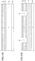
- Fig. 4 shows a structure of a semiconductor light emitting device according to a first embodiment of the invention.
- the n-type mesostructure PS layer (the first one conductivity type mesostructure PS layer) 13
- the n-type nanostructure PS layer (the first one conductivity type nanostructure PS layer ) 12 of 2 ⁇ m in thickness
- the p-type mesostructure PS layer (the opposite conductivity type mesostructure PS layer) 61 of 0.6 ⁇ m in thickness are formed in order on a n + type c-Si substrate 14.
- the translucent gold electrode 66 which serves as the anode is formed and on the back of the n + type c-Si substrate 14, the aluminum electrode 65 which serves as the cathode is formed.
- the direct current power supply 67 for the EL is connected between the anode 66 and the cathode 65.
- the thickness of the n-type nanostructure PS layer 12 acting as the EL actve layer is controlled into the thickness required from a design viewpoint correctly. And the promotion of "transformation of crystalline silicon to porous silicon" is performed sufficiently, so that the n-type nanostructure PS layer 12 becomes the completed nanostructure PS layer.
- the n-type nanostructure PS layer 12 is the layer that the non-degenerate n-type c-Si layer is transformed into a porous layer and the thickness of the n-type nanostructure PS layer 12 is controlled by the thickness of the non-degenerate n-type c-Si layer correctly.
- the p-type mesostructure PS layer 61 has a function to form the pn-junction between the n-type nanostructure PS layer 62 and the p-type mesostructure PS layer 61. Further, the p-type mesostructure PS layer 61 has a function to get better ohmic contact with the translucent gold electrode 66 formed on the p-type mesostructure PS layer 61.
- Fig. 5 shows a method for manufacturing a semiconductor light emitting device according to a first embodiment of the invention.
- the nanostructure PS is formed only on the portion of the non-degenerate n-type c-Si layer 22, and all the other portions becomes the mesostructure PS. Therefore, the thickness of the nanostructure PS layer 12 which is the light emitting layer is controlled into the thickness required from a design viewpoint correctly and "transformation of crystalline silicon to porous silicon" can be matured sufficiently.
- the thickness of the n-type nanostructure PS layer 12 can not be grown excessively over the thickness (2 ⁇ m, in the first embodiment of the invention) of the non-degenerate n-type c-Si layer 22 laminated in advance, but the mesostructure PS layer 13 whose resistivity is relatively low becomes thick even though the anodization time has lapsed beyond the time forming the optimum thickness of the nanostructure PS layer. Therefore, the completed nanostructure PS layer having the high quantum efficiency can be obtained by extending the anodization time sufficiently long to make progress of "transformation of crystalline silicon to porous silicon" sufficiently.
- the thickness of the nanostructure PS layer 12 can not be increased excessively even in the case that the excessive anodization time has lapsed, as well as "transformation of crystalline silicon to porous silicon" which is necessary and sufficient to improve the quantum efficiency of the nanostructure PS layer 12 is stimulated and the thickness is secured, whereby the series resistance Rs of the light emitting device being made can not be increased by a large amount than the value defined by the desired thickness of the nanostructure PS layer designed. Therefore, the semiconductor light emitting device having the high quantum efficiency as designed can be provided.
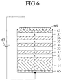
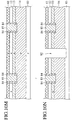
- Fig. 6 shows a structure of a semiconductor light emitting device according to a second embodiment of the invention.
- a fourth n-type mesostructure PS layer 13, a fourth n-type nanostructure PS layer 31, a third n-type mesostructure PS layer 32, a third n-type nanostructure PS layer 33, a second n-type mesostructure PS layer (the second one conductivity type mesostructure PS layer) 34, a second n-type nanostructure PS layer (the second one conductivity type nanostructure PS layer) 35, a first n-type mesostructure PS layer (the first one conductivity type mesostructure PS layer) 36, and a first n-type nanostructure PS layer (the first one conductivity type nanostructure PS layer) 37 are formed in this order on a n + type c-Si substrate 14.
- the thickness of the third to the first n-type mesostructure PS layer 32, 34 and 36 is 0.1 ⁇ m respectively.
- the thickness of the fourth to the first n-type nanostructure PS layer 31, 33, 35 and 37 is 0.5 ⁇ m respectively.
- the p-type mesostructure PS layer (the opposite conductivity type mesostructure PS layer) 61 of 0.6 ⁇ m in thickness further is formed on the first n-type nanostructure PS layer 37.
- the translucent gold electrode 66 which serves as the anode is formed and on the back of the n + type c-Si substrate 14, the aluminum electrode 65 which selves as the cathode is formed.
- the direct current power supply 67 for the EL is provided between the anode 66 and the cathode 65.
- the fourth to the first n-type nanostructure PS layer 31, 33, 35 and 37 act as the light emitting layers and in this case, these thickness are controlled into the thickness required from a design viewpoint correctly.
- the fourth to the first n-type nanostructure PS layer 31, 33, 35 and 37 are the layers that "transformation of crystalline silicon to porous silicon" of the non-degenerate n-type c-Si layer whose impurity concentration is low is made, and the thickness of the n-type nanostructure PS layer 12 is controlled by the thickness of the non-degenerate n-type c-Si layer established in advance correctly, and this thickness is controlled into the thickness required from a design viewpoint correctly and the promotion of "transformation of crystalline silicon to porous silicon" is performed sufficiently so that the high quantum efficiency is shown.
- the p-type mesostructure PS layer 61 has a function to form the pn-junction between the first n-type nanostructure PS layer 37 and the layer 61, and a function to get better ohmic contact with the translucent gold electrode 66.
- Fig. 7 shows a method for manufacturing a semiconductor light emitting device according to a second embodiment of the invention.
- the series resistance Rs can be reduced as compared with the semiconductor light emitting device having a single layer nanostructure PS layer of the same thickness as the total thickness of the four layers of the fourth to the first n-type nanostructure PS layer 31, 33, 35 and 37. This is caused by that as is described using Fig. 3, the series resistance Rs of the n-type nanostructure PS layer is increased in proportion to the square of the thickness.
- the series resistance Rs of the n-type nanostructure PS layer of 2 ⁇ m in thickness amounts to sixteen times of the series resistance Rs of the nanostructure PS layer of 0.5 ⁇ m in thickness.
- the entire series resistance Rs (total) amounts to only approximate four times of the single layer nanostructure PS layer of 0.5 ⁇ m in thickness.
- the entire series resistance Rs (total-div) of a stacked structure that the N layers of the n-type nanostructure PS layer of d/N in thickness are connected through the n-type mesostructure PS layer can be reduced to approximate 1/N with respect to the entire series resistance Rs (total-single) of the single layer nanostructure PS layer of "d" in thickness. It is the same as the case of the first embodiment that when being made by the method as shown in Fig.
- the n-type nanostructure PS layers 31, 33, 35 and 37 whose EL efficiency are high are formed only on the portions of the original non-degenerate n-type c-Si layer 41, 43, 45 and 47, whereby the correct film-thickness control and the sufficient "transformation of crystalline silicon to porous silicon" are stimulated, whereby the luminescence efficiency of the nanostructure PS layer can be improved.
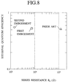
- Fig. 8 shows a relationship between an external quantum efficiency and a series resistance Rs of a semiconductor light emitting device (a symbol of ⁇ ) according to a second embodiment of the invention.
- Fig. 8 shows also relationships between an external quantum efficiency and series resistance of a semiconductor light emitting device (a symbol of ⁇ ) according to the prior art and the semiconductor light emitting device (a symbol of ⁇ ) according to the first embodiment of the invention.
- each of the semiconductor light emitting devices (the symbol of ⁇ ) according to the prior art, the first and the second embodiments of the invention are the same.
- the EL external quantum efficiency of each semiconductor light emitting device shown in Fig.8 are approximate same, in the respective series resistance Rs the significant difference is recognized.
- the series resistance Rs is largest as is 150k ⁇ .
- the series resistance Rs is reduced to 1/15 as is approximate 8k ⁇ .
- the series resistance Rs of the nanostructure PS layer 12 of the semiconductor light emitting device according to the second embodiment of the invention shown by the symbol of ⁇ is 1.6k ⁇ and is reduced to 1/5 as compared with the semiconductor light emitting device according to the first embodiment, thus, the smallest value is achieved.
- the reduction effect of the series resistance Rs of the nanostructure PS layer 12 of the semiconductor light emitting device according to the second embodiment of the invention is apparent.
- the PS layer can be made on the same c-Si substrate (wafer) to form a semiconductor integrated circuits (ICs). Therefore, the semiconductor device according to the invention can be integrated readily into the optoelectronic integrated circuits (OEIC) and the ICs such as a display device for an image display, thereby being applicable to various fields.
- OEIC optoelectronic integrated circuits
- a selective diffusion technology may be used for integration. That is, when the multi-layer diffused region constituted by the degenerate c-Si layer and the non-degenerate layer on the predetermined portion of the PS wafer is selectively formed, the semiconductor device structure according to the invention can be formed locally on the portion of the multi-layer diffused region.
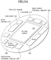
- Fig. 9A is a schematic view of a display device in which the PS light emitting diode (LED) array 101 of 512 x 512 dots is arranged on the central portion of the silicon wafer of 300 mm ⁇ in diameter, and the circuits such as a data driver 109 and a scan driver 115 for driving the PS light emitting diode (LED) array are formed on the periphery thereof.
- the PS light emitting diode (LED) array 101 of 512 x 512 dots is arranged on the central portion of the silicon wafer of 300 mm ⁇ in diameter, and the circuits such as a data driver 109 and a scan driver 115 for driving the PS light emitting diode (LED) array are formed on the periphery thereof.
- Fig. 9B is a block diagram showing a constitution of a display device shown in Fig.9A
- This display device is a gradation control type LED display device for controlling a lighting period of the PS light emitting diode (LED) arranged in a dot-matrix form.
- a data driver 109 is connected to the driver side of the PS LED array 101, and a scan driver 115 is connected to the scan side of the PS LED array 101.
- the display device shown in Fig.9B further has a data input control circuit 103, a RAM 105 connected to the data input control circuit 103, a gradation control circuit 107 connected between the data driver 109 and the data input control circuit 103.
- two-stage counter 111a and 111b, a decoder 113 connected between the counter 111b and the scan driver 115 are provided.
- the data input control circuit 103 fetches the predetermined display data and sends to the RAM 105 in synchronism with a clock signal CK1 during the time period that a selection signal SE turns in "H".
- the display data of 8 bits may be employed to represent one dot, to allow the light intensity of 255-step gradation for the one dot.
- the data are sent to the gradation control circuit 107.
- the gradation control circuit 107 controls the lighting duration of every dot based on the display data of 8 bits with 255-step gradation.
- the data driver 109 drives the 512 dots of the LED 101a simultaneously based on the lighting duration gradation-controlled.
- a signal which is sent from two-stage counter 111a and 111b which are reset by a reset signal Re and synchronizes with the dock signal CK1 is entered into the scan driver 115 via the decoder 113.
- the scan driver 115 scans this 512 dots of the LED 101a in order every time the 512 dots of the LED 101a is driven by the data driver 109.
- Fig. 9C is a schematically sectional view showing two dots of the LED matrix 101.
- a n-type c-Si buried layer 14 is formed on a p-type c-Si substrate 83.
- the n-type mesostructure PS layer (the first one conductivity type mesostructure PS layer) 13 ; the n-type nanostructure PS layer (the first one conductivity type nanostructure PS layer) 12 of approximate 1 to 2 ⁇ m in thickness ; and the p-type mesostructure PS layer (the opposite conductivity type mesostructure PS layer) 61 of approximate 0.6 to 1 ⁇ m in thickness are formed in order.
- the n-type c-Si buried layer 14, the n-type mesostructure PS layer 13, the n-type nanostructure PS layer 12 and the p-type mesostructure PS layer 61 are separated by a element isolation region 86 and are formed as a plurality of electrically independent regions, or LED dots.
- Plug electrodes 85 penetrate the p-type mesostructure PS layer 61, the n-type nanostructure PS layer 12 , the n-type mesostructure PS layer 13 and reach the n-type c-Si buried layers 14.
- the plug electrodes 85 serve as the cathodes of the respective LED dots 101a.
- This plug electrode 85 is formed by an impurity doped polysilicon (a doped polysilicon), refractory metals such as tungsten (W), molybdenum (Mo), titanium (Ti), or refractory metal silicides.
- Transparent electrodes 87 such as ITO films and SnO 2 films which serve as the respective anodes of the LED 101a dots are formed on the p-type mesostructure PS layers 61.
- the respective transparent electrodes 87 are connected to a scanning line 96 constituted by metals such as aluminum or aluminum alloy and the respective plug electrodes 85 are connected to data lines 89.
- the data line 89 also is constituted by metals such as aluminum or aluminum alloy.
- the data lines 89 and the transparent electrodes 87 are separated by first interlayer insulating films 88, the scanning line 96 and the data lines 89 are separated by second interlayer insulating films 95.
- the display device that the PS LED array 101 is arranged on the central portion of a large-diameter silicon wafer and peripheral circuits such as the drivers of the PS LED array 101 are arranged around the periphery of the silicon wafer is formed readily.
- the LED display device according to the third embodiment of the invention can be manufactured as follows.
- the structure that the n-type c-Si buried layer 14, the n-type mesostructure PS layer 13, the n-type nanostructure PS layer 12 and the p-type mesostructure PS layer 61 are formed in order on the p-type c-Si substrate 83 as shown in Fig. 10I can be realized.
- the degenerate n + type c-Si substrate 23, the non-degenerate n-type c-Si layer 22 and the degenerate p + type c-Si epitaxial growth layer 71 are formed by epitaxial growth on the p-type c-Si substrate 83.
- a groove which reaches the degenerate n + type c-Si substrate 23 from the back of the p-type c-Si substrate 83 is opened to provide the cathode to feed the anodizing current through the platinum electrode 3.
- a SDB method as shown in Fig.10F to Fig.10I is preferably used.
- a shielding region 142 as shown in Fig. 12 may be formed in the element isolation oxide film 85.
- Tungsten (W) may be used as the shielding region 142.
- the light is designed to be emitted from the upper surface efficiently by further arranging a Bragg mirror 141 constituted by quarter-wave dielectric stacks on the lower of the n-type c-Si buried layer 14.
- the Bragg mirror 141 may be sandwiched between the n-type c-Si buried layer 14 and the p-type c-Si substrate 83 by the SDB process.
- the structure that the light is designed to allow to emit toward the lower of the wafer by removing the c-Si substrate 83 of the bottom of the LED array section by etching may be taken.
- the non-degenerate n-type c-Si layer 22 and the degenerate p + type c-Si layer 71 may be formed on the degenerate n + type c-Si substrate of 300 mm diameter by epitaxial growth to finally remove the degenerate n + type c-Si substrate of the lower of the LED array section by etching
- the SDB method as shown in Fig.10F to Fig.10I is not required to use.
- the description is performed using the wafer of 300 mm (12 inches) in diameter as an example of the large-diameter wafer, it is as a matter of course that other wafer size such as 4 inches to 10 inches also may be used.
- the n-type nanostructure PS layer constituted by anodizing the non-degenerate n-type c-Si layer under light irradiation is used as the EL actve layer
- the p-type nanostructure PS layer constituted by anodizing the non-degenerate p-type c-Si layer may be used as a matter of course as the luminescence layer. In this case, it becomes the structure that all the p-type/the n-type in the first and the second embodiments are inverted.
- the tungsten lamp 5 shown in Fig. 5 and Fig.7 can be omitted.
- the value of the series resistance Rs of the p-type nanostructure PS layer is increased in proportion to the cube of the thickness of the p-type nanostructure PS layer, the multi-layer dividing effect becomes more significant by dividing into a plurality of thin layers shown in Fig.2.
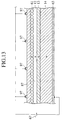
- the inexpensive and large area light emitting device can be formed by the array using the PS LED dots arranged in a matrix form. If the PS layers are not divided into a plurality of pieces so as to form the dot matrix, the light emitting device for interior illumination or the like that the entire surface of the silicon wafer of 4 inches to 12 inches in diameter serves as the light emitting region can be provided.
- Fig. 13 shows a partial section view of such light emitting device that the entire surface of the silicon wafer serves as the light emitting region.
- electrode wirings 97 having a low resistivity may be provided in the stripe shape on the transparent electrode 87 such as a ITO film and a SnO 2 film on the p-type mesostructure PS layer 61 as shown in Fig.12.
Landscapes
- Led Devices (AREA)
Applications Claiming Priority (3)
| Application Number | Priority Date | Filing Date | Title |
|---|---|---|---|
| JP24720597 | 1997-09-11 | ||
| JP24720597 | 1997-09-11 | ||
| JP247205/97 | 1997-09-11 |
Publications (3)
| Publication Number | Publication Date |
|---|---|
| EP0902486A2 true EP0902486A2 (de) | 1999-03-17 |
| EP0902486A3 EP0902486A3 (de) | 2000-10-25 |
| EP0902486B1 EP0902486B1 (de) | 2003-12-03 |
Family
ID=17160021
Family Applications (1)
| Application Number | Title | Priority Date | Filing Date |
|---|---|---|---|
| EP98117179A Expired - Lifetime EP0902486B1 (de) | 1997-09-11 | 1998-09-10 | Lichtemittierendes Halbleiterbauelement und Verfahren zu dessen Herstellung |
Country Status (3)
| Country | Link |
|---|---|
| US (2) | US6037612A (de) |
| EP (1) | EP0902486B1 (de) |
| DE (1) | DE69820184T2 (de) |
Cited By (3)
| Publication number | Priority date | Publication date | Assignee | Title |
|---|---|---|---|---|
| EP1251569A3 (de) * | 2001-04-17 | 2007-04-25 | Samsung Electronics Co., Ltd. | Lichtemittierende Vorrichtung und dessen Verwendung im lichtemittierendem Apparat |
| EP1328024A3 (de) * | 2002-01-10 | 2007-04-25 | Samsung Electronics Co. Ltd. | Optoelektronische Vorrichtung aus Silizium und Lichtemittierende Vorrichtung |
| EP1251568A3 (de) * | 2001-04-17 | 2008-02-27 | Samsung Electronics Co., Ltd. | LED und Display mit LEDs |
Families Citing this family (14)
| Publication number | Priority date | Publication date | Assignee | Title |
|---|---|---|---|---|
| US6599808B2 (en) * | 2001-09-12 | 2003-07-29 | Intel Corporation | Method and device for on-chip decoupling capacitor using nanostructures as bottom electrode |
| US6891202B2 (en) * | 2001-12-14 | 2005-05-10 | Infinera Corporation | Oxygen-doped Al-containing current blocking layers in active semiconductor devices |
| CN2686020Y (zh) * | 2004-01-19 | 2005-03-16 | 上海三思科技发展有限公司 | 一种高亮区比例的led点阵显示模块 |
| DE102004031135A1 (de) * | 2004-06-28 | 2006-01-19 | Infineon Technologies Ag | Resistives Halbleiterelement basierend auf einem Festkörperionenleiter |
| KR20070104158A (ko) * | 2006-04-21 | 2007-10-25 | 삼성전자주식회사 | 전자소자용 보호막 및 그 제조방법 |
| JP4347328B2 (ja) * | 2006-09-12 | 2009-10-21 | 株式会社沖データ | 半導体装置、ledヘッドおよび画像形成装置 |
| TW200919768A (en) * | 2007-10-19 | 2009-05-01 | Huga Optotech Inc | Semiconductor light-emitting device and method of fabricating the same |
| RU2364983C1 (ru) * | 2007-12-05 | 2009-08-20 | Общество С Ограниченной Ответственностью "Новые Энергетические Технологии" | Способ получения наноструктурированных кремниевых подложек |
| KR101478339B1 (ko) * | 2008-06-19 | 2015-01-08 | 서울바이오시스 주식회사 | 발광 소자 및 그 제조 방법 |
| JP4454689B1 (ja) * | 2009-09-10 | 2010-04-21 | 有限会社ナプラ | 発光ダイオード、発光装置、照明装置、ディスプレイ及び信号灯 |
| FR2967294B1 (fr) * | 2010-11-10 | 2012-12-07 | Commissariat Energie Atomique | Procédé de formation d'une structure multicouches |
| WO2017134438A1 (en) * | 2016-02-05 | 2017-08-10 | Bae Systems Plc | End effector for a robot |
| US11355549B2 (en) * | 2017-12-29 | 2022-06-07 | Lumileds Llc | High density interconnect for segmented LEDs |
| US11164917B1 (en) | 2018-09-14 | 2021-11-02 | Apple Inc. | Electronic devices with illuminated display borders |
Family Cites Families (3)
| Publication number | Priority date | Publication date | Assignee | Title |
|---|---|---|---|---|
| US5272355A (en) * | 1992-05-20 | 1993-12-21 | Spire Corporation | Optoelectronic switching and display device with porous silicon |
| JP3352118B2 (ja) * | 1992-08-25 | 2002-12-03 | キヤノン株式会社 | 半導体装置及びその製造方法 |
| DE4319413C2 (de) * | 1993-06-14 | 1999-06-10 | Forschungszentrum Juelich Gmbh | Interferenzfilter oder dielektrischer Spiegel |
-
1998
- 1998-09-09 US US09/150,276 patent/US6037612A/en not_active Expired - Fee Related
- 1998-09-10 EP EP98117179A patent/EP0902486B1/de not_active Expired - Lifetime
- 1998-09-10 DE DE69820184T patent/DE69820184T2/de not_active Expired - Fee Related
-
2000
- 2000-01-11 US US09/481,075 patent/US6403391B1/en not_active Expired - Fee Related
Cited By (3)
| Publication number | Priority date | Publication date | Assignee | Title |
|---|---|---|---|---|
| EP1251569A3 (de) * | 2001-04-17 | 2007-04-25 | Samsung Electronics Co., Ltd. | Lichtemittierende Vorrichtung und dessen Verwendung im lichtemittierendem Apparat |
| EP1251568A3 (de) * | 2001-04-17 | 2008-02-27 | Samsung Electronics Co., Ltd. | LED und Display mit LEDs |
| EP1328024A3 (de) * | 2002-01-10 | 2007-04-25 | Samsung Electronics Co. Ltd. | Optoelektronische Vorrichtung aus Silizium und Lichtemittierende Vorrichtung |
Also Published As
| Publication number | Publication date |
|---|---|
| EP0902486B1 (de) | 2003-12-03 |
| DE69820184D1 (de) | 2004-01-15 |
| EP0902486A3 (de) | 2000-10-25 |
| US6403391B1 (en) | 2002-06-11 |
| DE69820184T2 (de) | 2004-10-14 |
| US6037612A (en) | 2000-03-14 |
Similar Documents
| Publication | Publication Date | Title |
|---|---|---|
| US6037612A (en) | Semiconductor light emitting device having nanostructure porous silicon and mesostructure porous silicon | |
| US3947840A (en) | Integrated semiconductor light-emitting display array | |
| US7576404B2 (en) | Backlit photodiode and method of manufacturing a backlit photodiode | |
| US5583349A (en) | Full color light emitting diode display | |
| KR100268567B1 (ko) | 다중 파장으로 광을 발생시키기 위한 발광 다이오드의 모놀리식 어레이 및 이를 사용한 멀티 컬러 디스플레이 | |
| US5625201A (en) | Multiwavelength LED devices and methods of fabrication | |
| US8058091B2 (en) | Front lit PIN/NIP diode having a continuous anode/cathode | |
| JP4030614B2 (ja) | フル・カラ−発光ダイオ−ド表示装置 | |
| EP0618624B1 (de) | Licht emittierende Vorrichtung und Verfahren zu ihrer Herstellung | |
| JP2002512734A (ja) | オプトエレクトロニクス半導体ダイオード及びそれを備えた装置 | |
| EP1961051B1 (de) | Verfahren zur herstellung einer thermoelektrischen tunnelungsvorrichtung | |
| JPH1056201A (ja) | 基板構造、発光装置、基板構造の製造方法および発光装置の製造方法 | |
| JPH0645694A (ja) | 注入物をもつ頂部放出型vcsel | |
| JP2002359398A (ja) | 発光素子及びこれを適用したディスプレー装置 | |
| US20040164314A1 (en) | Semiconductor light emitting device | |
| WO2019199603A1 (en) | Led and vertical mos transistor formed on same substrate | |
| JP3490903B2 (ja) | 半導体発光素子およびその製造方法 | |
| US20080272418A1 (en) | Semiconductor component comprising a buried mirror | |
| TW201310538A (zh) | 氮化鎵發光二極體之快速熱退火 | |
| US4893154A (en) | Electroluminescent device | |
| KR20100130990A (ko) | 광전자 발광 구조 | |
| US6740904B2 (en) | Silicon light-emitting device and display apparatus employing the same | |
| TWI453953B (zh) | 氮化鎵發光二極體及其形成方法 | |
| JP3212686B2 (ja) | 半導体発光素子 | |
| IL274237A (en) | Method for controlling the amount of radiation with a predetermined wavelength for ingestion by a structure spread on a semiconductor |
Legal Events
| Date | Code | Title | Description |
|---|---|---|---|
| PUAI | Public reference made under article 153(3) epc to a published international application that has entered the european phase |
Free format text: ORIGINAL CODE: 0009012 |
|
| 17P | Request for examination filed |
Effective date: 19980910 |
|
| AK | Designated contracting states |
Kind code of ref document: A2 Designated state(s): DE FR |
|
| AX | Request for extension of the european patent |
Free format text: AL;LT;LV;MK;RO;SI |
|
| PUAL | Search report despatched |
Free format text: ORIGINAL CODE: 0009013 |
|
| AK | Designated contracting states |
Kind code of ref document: A3 Designated state(s): AT BE CH CY DE DK ES FI FR GB GR IE IT LI LU MC NL PT SE |
|
| AX | Request for extension of the european patent |
Free format text: AL;LT;LV;MK;RO;SI |
|
| AKX | Designation fees paid |
Free format text: DE FR |
|
| 17Q | First examination report despatched |
Effective date: 20010731 |
|
| GRAH | Despatch of communication of intention to grant a patent |
Free format text: ORIGINAL CODE: EPIDOS IGRA |
|
| GRAS | Grant fee paid |
Free format text: ORIGINAL CODE: EPIDOSNIGR3 |
|
| GRAA | (expected) grant |
Free format text: ORIGINAL CODE: 0009210 |
|
| AK | Designated contracting states |
Kind code of ref document: B1 Designated state(s): DE FR |
|
| REF | Corresponds to: |
Ref document number: 69820184 Country of ref document: DE Date of ref document: 20040115 Kind code of ref document: P |
|
| ET | Fr: translation filed | ||
| PLBE | No opposition filed within time limit |
Free format text: ORIGINAL CODE: 0009261 |
|
| STAA | Information on the status of an ep patent application or granted ep patent |
Free format text: STATUS: NO OPPOSITION FILED WITHIN TIME LIMIT |
|
| 26N | No opposition filed |
Effective date: 20040906 |
|
| PGFP | Annual fee paid to national office [announced via postgrant information from national office to epo] |
Ref country code: FR Payment date: 20050823 Year of fee payment: 8 |
|
| PGFP | Annual fee paid to national office [announced via postgrant information from national office to epo] |
Ref country code: DE Payment date: 20050912 Year of fee payment: 8 |
|
| PG25 | Lapsed in a contracting state [announced via postgrant information from national office to epo] |
Ref country code: DE Free format text: LAPSE BECAUSE OF NON-PAYMENT OF DUE FEES Effective date: 20070403 |
|
| REG | Reference to a national code |
Ref country code: FR Ref legal event code: ST Effective date: 20070531 |
|
| PG25 | Lapsed in a contracting state [announced via postgrant information from national office to epo] |
Ref country code: FR Free format text: LAPSE BECAUSE OF NON-PAYMENT OF DUE FEES Effective date: 20061002 |