EP0902559A2 - Procédé et dispositif pour l'extraction d'un signal d'horloge - Google Patents
Procédé et dispositif pour l'extraction d'un signal d'horloge Download PDFInfo
- Publication number
- EP0902559A2 EP0902559A2 EP98107429A EP98107429A EP0902559A2 EP 0902559 A2 EP0902559 A2 EP 0902559A2 EP 98107429 A EP98107429 A EP 98107429A EP 98107429 A EP98107429 A EP 98107429A EP 0902559 A2 EP0902559 A2 EP 0902559A2
- Authority
- EP
- European Patent Office
- Prior art keywords
- signal
- dispersion
- optical signal
- timing signal
- optical
- Prior art date
- Legal status (The legal status is an assumption and is not a legal conclusion. Google has not performed a legal analysis and makes no representation as to the accuracy of the status listed.)
- Granted
Links
Images












Classifications
-
- H—ELECTRICITY
- H04—ELECTRIC COMMUNICATION TECHNIQUE
- H04B—TRANSMISSION
- H04B10/00—Transmission systems employing electromagnetic waves other than radio-waves, e.g. infrared, visible or ultraviolet light, or employing corpuscular radiation, e.g. quantum communication
- H04B10/25—Arrangements specific to fibre transmission
- H04B10/2507—Arrangements specific to fibre transmission for the reduction or elimination of distortion or dispersion
- H04B10/2513—Arrangements specific to fibre transmission for the reduction or elimination of distortion or dispersion due to chromatic dispersion
- H04B10/2519—Arrangements specific to fibre transmission for the reduction or elimination of distortion or dispersion due to chromatic dispersion using Bragg gratings
-
- H—ELECTRICITY
- H04—ELECTRIC COMMUNICATION TECHNIQUE
- H04B—TRANSMISSION
- H04B2210/00—Indexing scheme relating to optical transmission systems
- H04B2210/25—Distortion or dispersion compensation
- H04B2210/252—Distortion or dispersion compensation after the transmission line, i.e. post-compensation
-
- H—ELECTRICITY
- H04—ELECTRIC COMMUNICATION TECHNIQUE
- H04L—TRANSMISSION OF DIGITAL INFORMATION, e.g. TELEGRAPHIC COMMUNICATION
- H04L7/00—Arrangements for synchronising receiver with transmitter
- H04L7/02—Speed or phase control by the received code signals, the signals containing no special synchronisation information
- H04L7/027—Speed or phase control by the received code signals, the signals containing no special synchronisation information extracting the synchronising or clock signal from the received signal spectrum, e.g. by using a resonant or bandpass circuit
-
- H—ELECTRICITY
- H04—ELECTRIC COMMUNICATION TECHNIQUE
- H04L—TRANSMISSION OF DIGITAL INFORMATION, e.g. TELEGRAPHIC COMMUNICATION
- H04L7/00—Arrangements for synchronising receiver with transmitter
- H04L7/02—Speed or phase control by the received code signals, the signals containing no special synchronisation information
- H04L7/033—Speed or phase control by the received code signals, the signals containing no special synchronisation information using the transitions of the received signal to control the phase of the synchronising-signal-generating means, e.g. using a phase-locked loop
Definitions
- the present invention relates in general to reproducing an electronic data signal from a received optical signal and more specifically to a method and device for extracting from the received optical signal, a timing signal for providing timing to the electric data signal reproduced from the received optical signal.
- Optical transmission systems with data rates of 10 Gb/s have been implemented in trunk-line optical communications.
- a further increase in transmission capacity is demanded.
- One way to achieve this is to increase transmission speeds using time-division multiplexing (including optical time-division multiplexing OTDM).
- Research and development for the next generation of transmission system, a 40-Gb/s system is being carried out vigorously throughout the world.
- the present invention is especially for use with this next generation system.
- the amount of total dispersion amount can be optimized as above using PLL (method (i)). That is, the above total dispersion optimization technique maximizes the intensity of the 40-GHz (data rate) component, and therefore the PLL method (method (i)) can be applied directly.
- a 40-Gb/s OTDM signal is formed by multiplexing two optical signals modulated with two 20-GHz RZ signals opposite in phase with their tails overlapping each other with the phases of their light waves shifted 180° relative to each other so as to cancel out the overlapping portions.
- the 40-GHz component is contained in the baseband spectrum. Accordingly, the total dispersion amount can be optimized using method (i). That is, in the case of the OTDM signal, when the above total dispersion optimization technique is applied, the amount of total dispersion is set to minimize intensity of the 40-GHz component. However, because the intensity of the 40-GHz component does not become zero at the minimum point, method (i) can be used to generate a timing signal from the optical signal whose chromatic dispersion has been optimized by the above technique.
- NRZ non-return-to-zero
- a frequency component equal in value to the signal bit rate does not exist in the baseband spectrum because of its principle of operation. Accordingly, method (i) cannot be applied, and usually the nonlinear extraction method (method of (ii)) is used. More specifically, if the above total dispersion amount optimization technique is applied to a 40-Gb/s NRZ system, the amount of total dispersion minimizes the 40-GHz frequency component, and because of its principle of operation, the intensity of the 40-GHz component becomes zero at the minimum point. Because the 40-GHz component cannot be extracted using method (i), it has been proposed to use method (ii).
- the extracted frequency component is to have a frequency equal in value to the bit rate of the received optical signal.
- the frequency component is extracted, the amount of total dispersion in the optical transmission line for signal reproduction is optimized. It is an object to provide a method and device that can do the foregoing even for an ultra high-speed optical signal transmitting at about 40-Gb/s and not containing a frequency component equal in value to the bit rate because of its principle of operation.
- timing signal extracting device uses a signal reproduction circuit to produce the data signal, a signal extraction circuit to extract the timing signal and a chromatic dispersion control apparatus to add dispersion compensation.
- the optical signal may be modulated by a data signal having a bit rate of X bits/second and the extracted timing signal may have a frequency of X hertz.
- the signal extraction circuit may be used with a phase locked loop.
- a voltage-controlled oscillator generates a clock signal
- a phase comparison circuit compares the phase of the clock signal with the phase of the extracted timing signal
- a control circuit controls the phase comparison circuit, to generate a control voltage for the voltage-controlled oscillator on the basis of the comparison.
- the chromatic dispersion control apparatus may use a variable dispersion compensator together with an optical detector which detects the intensity of a specific frequency component of the optical signal to minimize the intensity of the specific frequency component.
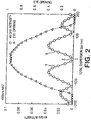
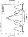
- Figs. 1 to 4 show computer simulation results of the dependence of the intensity of a 40-GHz component on total dispersion.
- the intensity of the 40-GHz component in the baseband spectrum is shown for an OTDM signal (a signal made by multiplexing two optical signals modulated with two 20-GHz RZ signals opposite in phase with their tails overlapping each other with the phases of their light waves shifted 180° relative to each other so as to cancel out the overlapping portions), an NRZ optical signal, an RZ optical signal (50% duty), and an RZ optical signal (25% duty), respectively, each with a data signal bit rate of 40-GHz.
- the eye opening amplitude is also shown in Figs. 1 to 4.
- the wavelength of input light was 1.55 ⁇ m, the power was -5 dBm on the average, the zero dispersion wavelength of the single-mode fiber (SMF) used was 1.3 ⁇ m, and the SMF length was 50 km; with these conditions, the amount of total dispersion was varied by varying the amount of dispersion in a DCF (dispersion-compensating fiber) connected in series with the SMF.
- SMF single-mode fiber
- the amount of total dispersion when the amount of total dispersion is set so that the intensity of the 40-GHz component is at a minimum in the case of the OTDM signal and at a maximum in the case of the RZ signals, the amount of total dispersion is approximately zero at the minimum or maximum. In either case, since the intensity of the 40-GHz component is not zero, the 40-GHz component can be extracted directly. In the case of the NRZ signal, on the other hand, if the amount of total dispersion is set in a similar manner, the intensity of the 40-GHz component becomes zero and the 40-GHz component cannot be extracted directly.
- Figs. 5 and 6 show the baseband spectra of optical modulated signals, in Figs. 5 and 6, for 40-Gb/s OTDM and NRZ signals, respectively.
- NRZ there is no 40-GHz component.
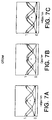
- Figs. 7A, 7B and 7C show waveform diagrams of the OTDM signal after being subjected to -40 ps/nm, 0 ps/nm and +40 ps/nm chromatic dispersion, respectively.
- Figs. 7A, 7B and 7C show waveform diagrams of the OTDM signal after being subjected to -40 ps/nm, 0 ps/nm and +40 ps/nm chromatic dispersion, respectively.
- Figs. 7A, 7B and 7C show waveform diagrams of the OTDM signal after being subjected to -40 ps/nm, 0 ps/nm and +40 ps/nm chromatic dispersion
- 8A, 8B and 8C show waveform diagrams of the NRZ signal after being subjected to -40 ps/nm, 0 ps/nm and +40 ps/nm chromatic dispersion, respectively.
- the "1" level at the center of the waveform rises but the cross points lower. From this it can be seen that there is a variation in intensity with a cycle equal to the length of one time slot. The variation in intensity creates the 40-GHz component.
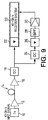
- Fig. 9 shows an optical transmission system equipped with a signal extraction circuit according to a first preferred embodiment of the present invention.
- a 40-Gb/s NRZ optical signal output from an optical transmitter 10 is amplified by an optical post-amplifier 12 and transmitted through an optical transmission line (optical fiber) 14.
- the received optical signal is amplified by an optical preamplifier 16 and input via a dispersion compensator 18 into a photodiode 22 in a 40-Gb/s receiver system 20.
- a portion of the optical signal directed to the photodiode 22 is separated by an optical coupler (not shown) and input into a photodiode 26 via a dispersion compensator 24.
- the 40-GHz component contained in the electrical signal output from the photodiode 26 is extracted by a narrowband band-pass filter 28, amplified by an amplifier 30, and supplied to the 40-Gb/s receiver system 20 as an extracted timing signal for data discrimination, etc.
- the dispersion compensator 18 has a dispersion value that reduces the total dispersion of the optical signal incident on the photodiode 22 to zero.
- the dispersion compensator 24 has a dispersion value of +60 ps/nm or -60 ps/nm. In this way, the eye opening of the input signal to the 40-Gb/s receiver system 20 is maximized. At the same time the 40-GHz frequency component is maximized for extraction by the narrowband band-pass filter 28.
- the dispersion compensator 18 may be omitted when the signal light wavelength is substantially equal to the zero dispersion wavelength of the optical fiber 14 and the eye opening of the input signal to the 40-Gb/s receiver system 20 is therefore sufficiently large even without the dispersion compensator 18.
- the dispersion compensators 18 and 24 need not necessarily have fixed dispersion values, but may be constructed as variable dispersion compensators having semi-fixed dispersion values that can be changed according to an external signal.
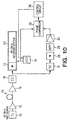
- Fig. 10 shows a second preferred embodiment of the present invention.
- the extracted 40-GHz component is not supplied directly to the 40-Gb/s receiver system 20.
- a voltage-controlled oscillator (VCO) 34 supplies a clock signal to the 40-Gb/s receiver system.
- the extracted 40-GHz timing signal and the clock signal output of VCO 34 are supplied to a phase comparator 32.
- Phase comparator 32 compares the phase of the extracted timing signal with that of the output of VCO 34.
- a control circuit 36 supplies a control voltage to the VCO 34 which thus generates the clock signal synchronized with the extracted 40-GHz component.
- the clock signal is supplied to the 40-Gb/s receiver system 20.
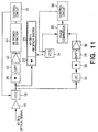
- Fig. 11 shows a third preferred embodiment of the present invention.
- a variable dispersion compensator 18' is used instead of the dispersion compensator 18 having a fixed or semi-fixed dispersion value.
- a portion of the optical signal directed to the photodiode 22 is separated by another optical coupler (not shown), supplied to photodiode 38 and converted by photodiode 38 into an electrical signal.
- a 40-GHz component is extracted by a band-pass filter 40 from the output of the photodiode 38.
- the 40-GHz component is amplified by an amplifier 42, and the power thereof is detected by a detector 44. Based on the value of the detected power, a control circuit 46 controls the amount of dispersion in the variable dispersion compensator 18' so as to minimize the power.
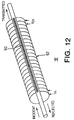
- variable dispersion compensator 18' M. M. Ohn et al., "Tunable fiber grating dispersion using a piezoelectric stack," OFC '97 Technical Digest, WJ3, pp. 155-156) will be described.
- a piezoelectric element 92 is attached to each of 21 segments of a chirped fiber grating 90.
- voltages V 1 to V 21 with a gradient as shown in Fig. 13, are applied to the piezoelectric elements 92, the pressure being applied in the longitudinal direction of the grating 90 changes.
- Voltages V 1 to V 21 are applied in accordance with the voltage patterns A to D shown in Fig. 13.
- Voltage patterns A to D produce the dispersion values (slopes of the lines) shown in Fig. 14. Dispersion values between those shown in Fig. 14 can be obtained for the transmission system shown in Fig. 11 by using voltage patterns between those shown in Fig. 13.
- Fig. 15 is a diagram showing one example of the control circuit 46 which could be used in the transmission system shown in Fig. 11.
- the intensity value of the 40-Gb/s frequency component is A/D converted by an A/D converter 94 and input as a digital signal to a microprocessor unit (MPU 96).
- the MPU 96 compares the present intensity value Ic with the previously received intensity value Ip stored in a memory 98, and checks to determine whether the relationship between the present dispersion amount and the intensity of the 40-Gb/s is on the X sloped portion or Y sloped portion of the intensity curve shown in Fig. 2.
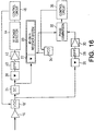
- Fig. 16 shows a first modification to the system shown in Fig. 11.
- the variable dispersion compensator 18' is controlled so that the amount of total dispersion is reduced to zero when the compensation amount of the variable dispersion compensator 18' is combined with that of the dispersion compensator 24.
- the dispersion compensator 24 is chosen to have a dispersion value of +60 ps/nm or -60 ps/nm, then the chromatic dispersion of the signal light entering the photodiode 26 is -60 ps/nm or + 60 ps/nm, respectively, to maximize the 40-GHz component.
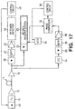
- Fig. 17 shows a second modification to the system shown in Fig. 11.
- a variable wavelength light source 48 is used in the optical transmitter 10.
- the wavelength of the signal light is controlled in such a manner so as to minimize the intensity of the extracted 40-GHz component, thereby making the wavelength of the signal light substantially equal to the zero dispersion wavelength of the optical fiber 14 and thus reducing the amount of total dispersion to zero.
- the wavelength dependence of the dispersion amount (dispersion slope) of the dispersion compensator 24 must be considered. It is also possible to configure the system such that the dispersion amount is controlled at a constant value against the changing signal light wavelength.
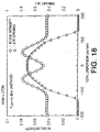
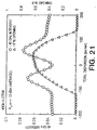
- Figs. 18 to 21 show (as simulation results) the relationship between the intensity of a 40-GHz component and the eye opening plotted against the amount of total dispersion (after dispersion compensation) when the transmitting optical power is 0, +5, + 10, and + 13 dBm, respectively, in a 50-km single mode fiber (SMF) transmission line of a 40-Gb/s OTDM signal.
- SMF single mode fiber
- the amount of total dispersion at which the intensity of the 40-GHz component is at a minimum coincides with the amount of total dispersion at which the eye opening is the largest only in the case of a linear transmission with a small signal light power (-5 dBm).
- the signal light power increases, the nonlinear effect becomes larger and the peaks separate such that displacement between the two increases.
- Fig. 22 is a graph illustrating the amount of total dispersion at which the eye opening is the largest and the amount of total dispersion at which the 40-GHz component is at a minimum, as a function of the transmitting optical power in the 50 km SMF transmission of the 40-Gb/s OTDM signal.
- the amount of total dispersion at which the 40-GHz component is at a minimum is not dependent on the transmitting optical power, but is kept constant at 0 ps/nm, whereas the amount of total dispersion at which the eye opening is the largest increases as the transmitting optical power increases.
- the eye opening can be maximized by adding an amount of chromatic dispersion determined based on the transmitting optical power.
- the 40-GHz component can be maximized by adding a prescribed fixed amount of dispersion compensation to the optical signal whose chromatic dispersion has been reduced to zero.
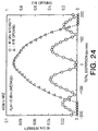
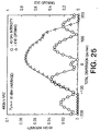
- Figs. 23 to 26 are graphs illustrating simulation results, for an NRZ signal.
- Figs. 23 to 26 show the relationship between the intensity of the 40-GHz component and the eye opening plotted against the amount of total dispersion (after dispersion compensation) when the transmitting optical power is 0, +5, + 10, and + 13 dBm, respectively, in a 50 km SMF transmission line.
- the amount of total dispersion at which the eye opening is the largest increases as the transmitting optical power increases. This characteristic is the same as that for the OTDM signal.
- variable dispersion compensator 18' cannot be controlled in such a manner as to bring the 40-GHz component to a minimum at zero total dispersion.
- variable dispersion compensator 18' can be controlled to bring the amount of total dispersion to zero by determining the midpoint between the two maxima.
- Fig. 27 shows a fourth preferred embodiment of the present invention.
- a control circuit 46' like the control circuit of Fig. 11, controls the chromatic dispersion of the optical signal to zero at the output of the variable dispersion compensator 18'. This minimizes the intensity of the detected 40-GHz component.
- the control circuit 46' sweeps the intensity of the 40-GHz component to determine the dispersion amounts for the two intensity peaks.
- the amount of dispersion compensation in the variable dispersion compensator 18' is set to have the dispersion compensation amount at the midpoint between the two maximum points. This minimizes the intensity of the 40-GHz frequency component at the output of the dispersion compensator 18' regardless of the transmitting optical power.
- a variable dispersion compensator VDC 50 maximizes the eye opening by adding an amount of chromatic dispersion determined according to the transmitting optical power.
- VDC 50 adds chromatic dispersion to the optical signal whose chromatic dispersion has been controlled to minimize the 40-GHz frequency component.
- the output of VDC 50 is supplied to the 40-Gb/s receiver system 20.
- Detection of the transmitting optical power can be achieved by separating a portion of the light output by the optical post-amplifier 12 and detecting its optical power using a photodiode.
- the transmitting optical power can be determined from power information supplied by the optical post-amplifier 12.
- the information concerning the optical output power is sent from the transmitting end (from post-amplifier 12), but as an alternative method, the optical power may be detected at the receiving end, or a monitor signal within the optical preamplifier 16 may be used.
- the system of Fig. 27 is constructed by modifying the system of Fig. 11 taking into consideration the nonlinear effect. It will be recognized that similar modifications can also be made to the systems of Figs. 16 and 17.
- the 40-GHz component becomes zero at periodic intervals.
- a receiver system in an ultra high-speed optical transmission system, can monitor and optimize the amount of chromatic dispersion using a variable dispersion compensator. This can be done while allowing the use of the PLL method for timing extraction even in the case of an NRZ signal.
Landscapes
- Physics & Mathematics (AREA)
- Electromagnetism (AREA)
- Engineering & Computer Science (AREA)
- Computer Networks & Wireless Communication (AREA)
- Signal Processing (AREA)
- Optical Communication System (AREA)
Applications Claiming Priority (3)
| Application Number | Priority Date | Filing Date | Title |
|---|---|---|---|
| JP24708697A JP3770711B2 (ja) | 1997-09-11 | 1997-09-11 | タイミング信号生成装置及び方法 |
| JP24708697 | 1997-09-11 | ||
| JP247086/97 | 1997-09-11 |
Publications (3)
| Publication Number | Publication Date |
|---|---|
| EP0902559A2 true EP0902559A2 (fr) | 1999-03-17 |
| EP0902559A3 EP0902559A3 (fr) | 2004-02-11 |
| EP0902559B1 EP0902559B1 (fr) | 2004-12-29 |
Family
ID=17158226
Family Applications (1)
| Application Number | Title | Priority Date | Filing Date |
|---|---|---|---|
| EP98107429A Expired - Lifetime EP0902559B1 (fr) | 1997-09-11 | 1998-04-23 | Procédé et dispositif pour l'extraction d'un signal d'horloge |
Country Status (5)
| Country | Link |
|---|---|
| US (1) | US6204949B1 (fr) |
| EP (1) | EP0902559B1 (fr) |
| JP (1) | JP3770711B2 (fr) |
| CN (1) | CN1196283C (fr) |
| DE (1) | DE69828347T2 (fr) |
Cited By (3)
| Publication number | Priority date | Publication date | Assignee | Title |
|---|---|---|---|---|
| EP1179900A1 (fr) * | 2000-08-11 | 2002-02-13 | Alcatel | Récepteur optique avec récupération d' horloge du signal d'entrée et un correcteur supplémentaire de phase de l'horloge récupérée |
| WO2004004171A1 (fr) * | 2002-06-26 | 2004-01-08 | Axe, Inc. | Compensation de dispersion dynamique dans des systemes de transmission optique a vitesse elevee |
| EP1819070A1 (fr) * | 2006-02-09 | 2007-08-15 | Alcatel Lucent | Circuit et procédé de récupération d'horloge pour un récepteur optique |
Families Citing this family (22)
| Publication number | Priority date | Publication date | Assignee | Title |
|---|---|---|---|---|
| EP0948151B1 (fr) | 1998-03-30 | 2006-02-01 | Fujitsu Limited | Méthode de réglage de la longueur d'onde de signal d'un système de transmission optique |
| FR2791835B1 (fr) * | 1999-03-31 | 2001-06-29 | Cit Alcatel | Dispositif et procede de compensation de la dispersion de polarisation dans un systeme de transmission optique |
| IT1310666B1 (it) * | 1999-08-03 | 2002-02-19 | Cselt Centro Studi Lab Telecom | Ricevitore per segnali a flusso discontinuo e relativo procedimento diricezione. |
| US6792209B1 (en) * | 1999-12-22 | 2004-09-14 | At&T Corp. | Method and system for reducing non-linear cross talk in low dispersion optical fiber |
| US7058311B1 (en) * | 2002-03-15 | 2006-06-06 | Xtera Communications, Inc. | System and method for dispersion compensation in an optical communication system |
| US6819478B1 (en) | 2002-03-15 | 2004-11-16 | Xtera Communications, Inc. | Fiber optic transmission system with low cost transmitter compensation |
| US7197245B1 (en) | 2002-03-15 | 2007-03-27 | Xtera Communications, Inc. | System and method for managing system margin |
| DE10216281B4 (de) * | 2002-04-12 | 2007-04-12 | Noé, Reinhold, Prof. Dr.-Ing. | Anordnung und Verfahren für eine Dispersionsdetektion |
| JP4082992B2 (ja) * | 2002-11-21 | 2008-04-30 | 富士通株式会社 | 光分散モニタ装置および方法、並びに、それを用いた光伝送システム |
| CA2427416C (fr) * | 2003-05-01 | 2010-11-16 | 101039130 Saskatchewan Ltd. | Dispositif de direction pour outils remorques |
| US20040234275A1 (en) * | 2003-05-20 | 2004-11-25 | Aref Chowdhury | Process for optical communication and system for same |
| JP2005159928A (ja) * | 2003-11-28 | 2005-06-16 | Hitachi Communication Technologies Ltd | 自動分散補償方法 |
| US7454144B2 (en) * | 2003-12-05 | 2008-11-18 | Lucent Technologies Inc. | Low total excursion dispersion maps |
| JP4464959B2 (ja) * | 2004-02-20 | 2010-05-19 | 富士通株式会社 | 分散補償方法及び分散補償装置 |
| JP2005341392A (ja) * | 2004-05-28 | 2005-12-08 | Fujitsu Ltd | 光伝送装置、光伝送システムおよび分散補償方法 |
| WO2006126918A1 (fr) * | 2005-05-24 | 2006-11-30 | St. Jude Medical Ab | Procede et dispositif medical d'evaluation de la prevalence de differentes postures d'un patient et support lisible par ordinateur faisant executer le procede a un ordinateur |
| US20080212658A1 (en) * | 2007-03-01 | 2008-09-04 | Ahmadreza Rofougaran | Method and system for communication of signals using a direct digital frequency synthesizer (ddfs) |
| JP2009117921A (ja) * | 2007-11-01 | 2009-05-28 | Sumitomo Electric Ind Ltd | 光受信器、及び、光受信器の制御方法 |
| JP5458826B2 (ja) * | 2009-11-24 | 2014-04-02 | 富士通株式会社 | 分散補償装置、光受信装置、分散補償方法および光受信方法 |
| CN103620986B (zh) * | 2011-01-24 | 2016-11-16 | 日本电信电话株式会社 | 波长色散量推测方法、波长色散补偿电路以及接收装置 |
| JP6687939B2 (ja) * | 2016-01-15 | 2020-04-28 | 国立研究開発法人情報通信研究機構 | 光電変換器 |
| US11606150B2 (en) * | 2020-06-23 | 2023-03-14 | Infinera Corporation | Data synchronization in optical networks and devices |
Family Cites Families (6)
| Publication number | Priority date | Publication date | Assignee | Title |
|---|---|---|---|---|
| JPH06216467A (ja) | 1993-01-19 | 1994-08-05 | Hitachi Ltd | 半導体光分散補償器 |
| US5574588A (en) * | 1994-02-23 | 1996-11-12 | Nippon Telegraph And Telephone Corporation | Phase lock loop circuit using optical correlation detection |
| EP0684709B1 (fr) | 1994-05-25 | 2002-10-02 | AT&T Corp. | Système de communication optique avec compensation de dispersion ajustable |
| JP3846918B2 (ja) * | 1994-08-02 | 2006-11-15 | 富士通株式会社 | 光伝送システム、光多重伝送システム及びその周辺技術 |
| JPH08256106A (ja) | 1995-03-17 | 1996-10-01 | Fujitsu Ltd | 光増幅海底伝送システムの分散補償装置 |
| JP3522044B2 (ja) | 1996-04-19 | 2004-04-26 | 富士通株式会社 | 光伝送システム |
-
1997
- 1997-09-11 JP JP24708697A patent/JP3770711B2/ja not_active Expired - Fee Related
-
1998
- 1998-04-09 US US09/057,597 patent/US6204949B1/en not_active Expired - Fee Related
- 1998-04-23 DE DE69828347T patent/DE69828347T2/de not_active Expired - Fee Related
- 1998-04-23 EP EP98107429A patent/EP0902559B1/fr not_active Expired - Lifetime
- 1998-05-15 CN CN98108450.8A patent/CN1196283C/zh not_active Expired - Fee Related
Cited By (4)
| Publication number | Priority date | Publication date | Assignee | Title |
|---|---|---|---|---|
| EP1179900A1 (fr) * | 2000-08-11 | 2002-02-13 | Alcatel | Récepteur optique avec récupération d' horloge du signal d'entrée et un correcteur supplémentaire de phase de l'horloge récupérée |
| US6816684B2 (en) | 2000-08-11 | 2004-11-09 | Alcatel | Method of generating a clock signal of exact phase from an optical input signal and optical receiver therefor |
| WO2004004171A1 (fr) * | 2002-06-26 | 2004-01-08 | Axe, Inc. | Compensation de dispersion dynamique dans des systemes de transmission optique a vitesse elevee |
| EP1819070A1 (fr) * | 2006-02-09 | 2007-08-15 | Alcatel Lucent | Circuit et procédé de récupération d'horloge pour un récepteur optique |
Also Published As
| Publication number | Publication date |
|---|---|
| DE69828347T2 (de) | 2005-10-13 |
| JPH1188262A (ja) | 1999-03-30 |
| JP3770711B2 (ja) | 2006-04-26 |
| EP0902559B1 (fr) | 2004-12-29 |
| US6204949B1 (en) | 2001-03-20 |
| EP0902559A3 (fr) | 2004-02-11 |
| CN1211117A (zh) | 1999-03-17 |
| DE69828347D1 (de) | 2005-02-03 |
| CN1196283C (zh) | 2005-04-06 |
Similar Documents
| Publication | Publication Date | Title |
|---|---|---|
| EP0902559B1 (fr) | Procédé et dispositif pour l'extraction d'un signal d'horloge | |
| US6501580B1 (en) | Method and apparatus for optimizing dispersion in an optical fiber transmission line in accordance with an optical signal power level | |
| US6594070B2 (en) | Optical communication system, optical receiver and wavelength converter | |
| US6411416B1 (en) | Method and apparatus for minimizing the intensity of a specific frequency component of an optical signal travelling through an optical fiber transmission line to thereby minimize the total dispersion | |
| JP5157521B2 (ja) | 偏波多重光受信機、偏波多重光送受信システムおよび偏波多重光送受信システムの制御方法 | |
| JP3910003B2 (ja) | 光受信局、光通信システム及び分散制御方法 | |
| JP4516907B2 (ja) | 光受信装置およびその制御方法 | |
| US7224911B2 (en) | Adaptive distortion compensation in optical fiber communication networks | |
| CN100539472C (zh) | 信号波形劣化补偿器 | |
| US20040213578A1 (en) | Chromatic dispersion compensation controlling system | |
| JP4582874B2 (ja) | 偏波モード分散補償方法および偏波モード分散補償装置 | |
| US7620326B2 (en) | Method for transmitting at least one first and second data signal in polarization multiplex in an optical transmission system | |
| JPWO2001015347A1 (ja) | 光通信システム、光受信器および波長変換器 | |
| EP0902560B1 (fr) | Procédé et dispositif pour optimiser la dispersion d'une ligne de transmission à fibre optique selon un niveau de puissance de signal optique | |
| US20040062336A1 (en) | Timing extraction circuit for use in optical receiver that uses clock of frequency equal to one half of data transmission rate, and duty cycle deviation handling circuit for use in optical transmitter and receiver | |
| US7609974B2 (en) | Data transmission method and a system thereof | |
| JP3498839B2 (ja) | 光通信用受信器 | |
| JP3487217B2 (ja) | 光送信器及びそれを用いた光伝送装置 | |
| JP4056846B2 (ja) | 分散モニタ装置、分散モニタ方法および自動分散補償システム | |
| JP2000321171A (ja) | 分散測定装置および分散測定方法 | |
| KR20020054212A (ko) | 전자 소자에 대한 의존도를 줄인 광전송 장치 및 광수신장치 | |
| JP2002204210A (ja) | 光受信器及び光受信方法 | |
| JP4130342B2 (ja) | 光信号処理装置 | |
| EP1344340A2 (fr) | Demultiplexeur de signaux a haut debit de donnees |
Legal Events
| Date | Code | Title | Description |
|---|---|---|---|
| PUAI | Public reference made under article 153(3) epc to a published international application that has entered the european phase |
Free format text: ORIGINAL CODE: 0009012 |
|
| AK | Designated contracting states |
Kind code of ref document: A2 Designated state(s): AT BE CH CY DE DK ES FI FR GB GR IE IT LI LU MC NL PT SE |
|
| AX | Request for extension of the european patent |
Free format text: AL;LT;LV;MK;RO;SI |
|
| PUAL | Search report despatched |
Free format text: ORIGINAL CODE: 0009013 |
|
| AK | Designated contracting states |
Kind code of ref document: A3 Designated state(s): AT BE CH CY DE DK ES FI FR GB GR IE IT LI LU MC NL PT SE |
|
| AX | Request for extension of the european patent |
Extension state: AL LT LV MK RO SI |
|
| RIC1 | Information provided on ipc code assigned before grant |
Ipc: 7H 04B 10/158 B Ipc: 7H 04B 10/18 A |
|
| GRAP | Despatch of communication of intention to grant a patent |
Free format text: ORIGINAL CODE: EPIDOSNIGR1 |
|
| 17P | Request for examination filed |
Effective date: 20040521 |
|
| AKX | Designation fees paid |
Designated state(s): DE FR GB |
|
| GRAS | Grant fee paid |
Free format text: ORIGINAL CODE: EPIDOSNIGR3 |
|
| GRAA | (expected) grant |
Free format text: ORIGINAL CODE: 0009210 |
|
| AK | Designated contracting states |
Kind code of ref document: B1 Designated state(s): DE FR GB |
|
| REG | Reference to a national code |
Ref country code: GB Ref legal event code: FG4D |
|
| REG | Reference to a national code |
Ref country code: IE Ref legal event code: FG4D |
|
| REF | Corresponds to: |
Ref document number: 69828347 Country of ref document: DE Date of ref document: 20050203 Kind code of ref document: P |
|
| PGFP | Annual fee paid to national office [announced via postgrant information from national office to epo] |
Ref country code: FR Payment date: 20050308 Year of fee payment: 8 |
|
| PGFP | Annual fee paid to national office [announced via postgrant information from national office to epo] |
Ref country code: GB Payment date: 20050420 Year of fee payment: 8 |
|
| PGFP | Annual fee paid to national office [announced via postgrant information from national office to epo] |
Ref country code: DE Payment date: 20050425 Year of fee payment: 8 |
|
| PLBE | No opposition filed within time limit |
Free format text: ORIGINAL CODE: 0009261 |
|
| STAA | Information on the status of an ep patent application or granted ep patent |
Free format text: STATUS: NO OPPOSITION FILED WITHIN TIME LIMIT |
|
| ET | Fr: translation filed | ||
| 26N | No opposition filed |
Effective date: 20050930 |
|
| PG25 | Lapsed in a contracting state [announced via postgrant information from national office to epo] |
Ref country code: GB Free format text: LAPSE BECAUSE OF NON-PAYMENT OF DUE FEES Effective date: 20060423 |
|
| PG25 | Lapsed in a contracting state [announced via postgrant information from national office to epo] |
Ref country code: DE Free format text: LAPSE BECAUSE OF NON-PAYMENT OF DUE FEES Effective date: 20061101 |
|
| GBPC | Gb: european patent ceased through non-payment of renewal fee |
Effective date: 20060423 |
|
| REG | Reference to a national code |
Ref country code: FR Ref legal event code: ST Effective date: 20061230 |
|
| PG25 | Lapsed in a contracting state [announced via postgrant information from national office to epo] |
Ref country code: FR Free format text: LAPSE BECAUSE OF NON-PAYMENT OF DUE FEES Effective date: 20060502 |