EP0903060B1 - Dispositif et procede de montage d'un composant electronique sur un substrat - Google Patents
Dispositif et procede de montage d'un composant electronique sur un substrat Download PDFInfo
- Publication number
- EP0903060B1 EP0903060B1 EP97906616A EP97906616A EP0903060B1 EP 0903060 B1 EP0903060 B1 EP 0903060B1 EP 97906616 A EP97906616 A EP 97906616A EP 97906616 A EP97906616 A EP 97906616A EP 0903060 B1 EP0903060 B1 EP 0903060B1
- Authority
- EP
- European Patent Office
- Prior art keywords
- electronic component
- substrate
- component according
- region
- fluid
- Prior art date
- Legal status (The legal status is an assumption and is not a legal conclusion. Google has not performed a legal analysis and makes no representation as to the accuracy of the status listed.)
- Expired - Lifetime
Links
Images

Classifications
-
- H—ELECTRICITY
- H05—ELECTRIC TECHNIQUES NOT OTHERWISE PROVIDED FOR
- H05K—PRINTED CIRCUITS; CASINGS OR CONSTRUCTIONAL DETAILS OF ELECTRIC APPARATUS; MANUFACTURE OF ASSEMBLAGES OF ELECTRICAL COMPONENTS
- H05K1/00—Printed circuits
- H05K1/18—Printed circuits structurally associated with non-printed electric components
-
- H—ELECTRICITY
- H10—SEMICONDUCTOR DEVICES; ELECTRIC SOLID-STATE DEVICES NOT OTHERWISE PROVIDED FOR
- H10W—GENERIC PACKAGES, INTERCONNECTIONS, CONNECTORS OR OTHER CONSTRUCTIONAL DETAILS OF DEVICES COVERED BY CLASS H10
- H10W40/00—Arrangements for thermal protection or thermal control
- H10W40/40—Arrangements for thermal protection or thermal control involving heat exchange by flowing fluids
- H10W40/47—Arrangements for thermal protection or thermal control involving heat exchange by flowing fluids by flowing liquids, e.g. forced water cooling
- H10W40/475—Arrangements for thermal protection or thermal control involving heat exchange by flowing fluids by flowing liquids, e.g. forced water cooling using jet impingement
-
- H—ELECTRICITY
- H05—ELECTRIC TECHNIQUES NOT OTHERWISE PROVIDED FOR
- H05K—PRINTED CIRCUITS; CASINGS OR CONSTRUCTIONAL DETAILS OF ELECTRIC APPARATUS; MANUFACTURE OF ASSEMBLAGES OF ELECTRICAL COMPONENTS
- H05K1/00—Printed circuits
- H05K1/18—Printed circuits structurally associated with non-printed electric components
- H05K1/182—Printed circuits structurally associated with non-printed electric components associated with components mounted in printed circuit boards [PCB], e.g. insert-mounted components [IMC]
Definitions
- This invention relates generally to electronic components, and, more particularly, to an apparatus and method for mounting an electronic component to a substrate and to a method for spray-cooling an electronic component mounted to a substrate.
- Electronic modules such as printed circuit boards (PCBs), multi-chip modules (MCMs) and electronic hybrid assemblies are generally comprised of a number of individual electronic components such as integrated circuits, passive components and power transistors, mounted to a common substrate.
- the individual electronic components may be heat sources which require cooling during normal operation as well as during testing and tuning.
- Evaporative spray cooling features the spraying of atomized fluid droplets directly or indirectly onto a surface of a heat source such as an electronic component.
- a heat source such as an electronic component.
- evaporative spray cooling is a preferred method of heat removal in many electronics applications
- known spray cooling systems are generally designed to cool entire surfaces of large electronic modules. Because fluid is typically sprayed directly onto the surface of electronic modules, the fluid may capture particulate matter from the electronic components, such as flux residue, which can clog nozzles and impede the effective spraying of the fluid. In addition, heat-producing electronic components may be isolated in areas of electronic modules which have otherwise low heat-loads, so that spray-cooling an entire electronic module may not be desirable or practical.
- US 4,658,330 discloses a unitary electronic circuit element that has an interconnect surface at which it is provided with contact pads and is mounted on a circuit board using a flexible, sheet-form interconnect member that comprises dielectric material and runs of electrically conductive material. Each conductor run extends between a contact pad that is exposed at a first main face of the interconnect member and a termination point that is exposed at a second main face of the interconnect member.
- the interconnect surface of the electronic circuit element and the second main face of the interconnect member are placed in mutually confronting relationship, and the circuit element is attached to the second main face of the interconnect member by way of its interconnect surface, whereby electrically conductive contact is established between the contact pads of the circuit element and the corresponding termination points of the interconnect member.
- the circuit element is attached by way of its back face to a thermally conductive plate that has, at one main face, pressure pads that at least partially surround a circuit element receiving area of the plate.
- the first main face of the interconnect member and the main face of the circuit board are placed in mutually confronting relationship, with the contact pads of the interconnect member touching corresponding contact pads of the circuit board.
- the plate and the circuit board are clamped together, whereby the pressure pads supply contact force to maintain the contact pads of the interconnect member in electrically conductive pressure contact with the corresponding contact pads of the circuit board.
- US 5,220,804 discloses a compact spray cooling system for cooling a heat source or a plurality of heat sources.
- the system uses at least one atomizer arranged in an array to deliver a fine spray across a wide distribution to impinge upon the surface to be cooled.
- the spray maintains a thin liquid film upon the cooled surface where heat is transferred in a phase change process.
- the liquid and vapor resulting from the heat transfer process is removed from the system at the edges of the heat source(s) and uses the momentum of the original spray to move the vapor and liquid to a fluid removal port.
- the use of the momentum of the spray to remove the liquid from the system allows the system to be gravity independent and used in transportation, avionics, and spacecraft applications where adverse gravity conditions exist.
- the atomizer array can be spaced closely to the heat source because the individual atomizers develop the spray in a relatively short distance.
- the present invention provides an electronic component, as claimed in claim 1.
- FIG. 1 is a perspective view of a typical electronic component 10, which includes a device pedestal 12, or flange; a number of terminals 14; a cover 16 and one or more dies (not shown), which are protected by cover 16.
- Electronic component 10 may be, for example, an NPN Silicon Radio Frequency (RF) Power Transistor, available from Motorola, order number MRF899/D. References to electronic component 10 will be understood to apply not only to component 10 as depicted in FIG. 1, but also to differently-configured power transistors such as a flangeless RF power transistor, available from Motorola, order number SRF7016, illustrated in FIG. 2.
- RF Radio Frequency
- electronic component 10 includes terminals 14; cover 16; a base 17 such as alumina, which has a slight thickness and which extends slightly from cover 16; and one or more dies (not shown), which may be, for example, a transistor base, an transistor emitter and a transistor collector. Dies 22 are enclosed by cover 16.
- Component 10 depicted in FIG. 2 unlike component 10 depicted in FIG. 1, does not include flange 12.
- FIG. 3 is a front view along line 3-3 of electronic component 10 depicted in FIG. 1, illustrating a typical manner of mounting component 10 to a substrate 18 using a carrier plate 19.
- Substrate 18 comprises one or more layers of glass-filled epoxy, teflon, alumina, ceramic or plastic.
- Carrier plate 19 is made, for example, of copper, aluminum-silicon carbide (AlSiC) or graphite.
- terminals 14 are in communication with a first side 20 of substrate 18. Terminals 14 may be attached to substrate 18 or to another device (not shown) located on substrate 18 in a variety of ways, such as soldering or conductive epoxy.
- Cover 16 which encloses at least one heat-generating die 22, is coupled to terminals 14 and is positioned on first side 20 of substrate 18.
- Flange 12 which may provide an electrical grounding surface and enhanced heat spreading for die 22, may be secured to carrier plate 19 in a variety of ways, using screws, for example. Die 22, therefore, is typically surrounded by cover 16 on one side and by flange 12 on the other.
- electronic component 10 illustrated in FIG. 2, is mounted to carrier plate 19 and substrate 18 in a typical manner.
- Base 17 of component 10 extends at least in part into substrate 18.
- Terminals 14 are in communication with first side 20 of substrate 18.
- Terminals 14 may be attached to substrate 18 or to a device (shown in FIG. 3) located on substrate 18 in a variety of ways, such as soldering or conductive epoxy.
- Cover 16 which protects at least one heat-generating die 22 (not shown), is coupled to terminals 14 and is located on first side 20 of substrate 18.
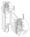
- FIGs. 5 and 6 are front views of electronic component 10 as depicted in FIGs. 2 and 4, rotated 180 degrees relative to the plane of substrate 18, in accordance with a preferred embodiment of the present invention.
- component 10 is reverse-mounted with respect to the traditional mounting technique.
- a passage 26 extends through substrate 18 and carrier plate 19, if present (carrier plate 19 is not shown in FIGs. 5 and 6, and for simplicity, both substrate 18 and the combination of substrate 18 and carrier plate 19 will be referred to hereafter as simply substrate 18), from first side 20 to a second side 82 of substrate 18.
- Passage 26 may be cylindrical, rectangular or of another suitable shape.
- Cover 16 which preferably includes a fixed portion 28, such as a wall, and a removable portion 24, encloses die 22 and a least a portion of terminals 14.
- Fixed portion 28 is preferably ceramic, but may be another suitable material such as high-temperature plastic or liquid-crystal polymer.
- Removable portion 24 is preferably plastic, but likewise may be made of another material, such as ceramic or metal fill. Removable portion 24 is detachably connected to fixed portion 28, and may, for example, snap onto fixed portion 28 via flange 21 and bump 35, or may be secured with an adhesive (not shown), and then be peeled off.
- Fixed portion 28 is preferably secured to terminal 14 at a connection region 27 using an epoxy 25, such as a B-staged epoxy.
- an epoxy 25 such as a B-staged epoxy.
- Terminal 14 may be soldered or otherwise secured to first side 20 of substrate 18, via a metallization region 23 on terminal 14, for example.
- An extension region 30 of fixed portion 28 has a surface which is substantially coplanar with second side 82 of substrate 18, the extension region 28 and substrate 18 having a space 32 therebetween, so that passage 26 is not completely filled.
- An adhesive material 34 for example, a polyamid hotmelt material, such materials being well-known and widely available, is disposed on the surface of extension region 28, a portion of adhesive 34 preferably extending into space 32.
- a sealing frame 36 which is connected to second side 82 of substrate 18 and overlaps space 32, is also in contact with adhesive 34. Sealing frame 36 is preferably a metallic frame such as brass which surrounds passage 26, covering space 32. Sealing frame 36 may be soldered to second side 82 using high-temperature solder, but may also be ultrasonically welded or laser-welded to second side 82, or attached using an adhesive such as silicone or another high-temperature adhesive.
- solder paste may be applied to first side 20 of substrate 18 in the area of terminals 14 using a well-known method such as screen-printing. Then, component 10, including adhesive 34 which may be pre-formed in the shape of a gasket and disposed on the surface of extension region 28, may be placed cover-side down within passage 26, so that adhesive 34 contacts sealing frame 36. Next, the entire assembly may be heated using a standard temperature reflow profile. When the solder paste melts, terminals 14 are electrically joined. When adhesive 34 melts, a hermetic seal is formed between fixed portion 28 of cover 16 and second side 82 of substrate 18. To ensure that removable portion 24 of cover 16 remains detachable, removable portion 24 may be treated with a mold-release material (not shown), such materials being well-known and widely available, prior to the reflow process.
- a mold-release material not shown
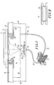
- FIG. 7 is a side-view of electronic component 10 mounted as shown in FIGs. 5 and 6, removable portion 24 of cover 16 having been removed, which further depicts a spray-cooling system having a closed-loop fluid flow.
- a housing 40 having a side surface 42 and a top surface 44 and defining a chamber 45 is coupled to second side 82 of substrate 18.
- Housing 40 is preferably rectangular, but may be another geometrical shape, such as cylindrical, and is preferably plastic, but may be constructed from another suitable material such as metal.
- Housing 40 may also include an electromagnetic interference-attenuating material (not shown).
- One or more nozzles 60 are preferably disposed in top surface 44 of housing 40.
- a single nozzle 60 is shown.
- Nozzle 60 has a receptacle end 62, which is in communication with a fluid inlet port 46; a spray end 64, which includes an aperture 66, preferably on the order of 0.15mm in diameter; and a swirl plate or insert 68.
- Swirl plate 68 may be secured to receptacle end 62 by, for example, press-fitting, soldering or bonding. It will be appreciated, however, that nozzle 60, along with swirl plate 68, may be integrally formed in housing 40.
- Nozzle 60 is preferably a miniature atomizer such as a simplex pressure-swirl atomizer, which is approximately 1.5mm high, and may be made of any suitable material.
- a suitable material is a metal such as brass or stainless steel.
- Simplex pressure-swirl atomizers are described in detail in U.S. Patent No. 5,220,804 to Tilton et al., and are commercially available from Isothermal Systems Research, Inc., located in Colton, Washington.
- a fluid pump 50 which is connected via tube 52 to fluid inlet port 46, supplies a coolant fluid to receptacle end 62 of nozzle 60, which has been fitted with swirl plate 68.
- Spray end 64 atomizes the coolant and discharges an atomized fluid 70 through aperture 66 into chamber 45 and onto one or more dies 22.
- Fluid 45 may be discharged from aperture 66 at an angle to top surface 44, preferably at a substantially perpendicular angle to top surface 44.
- atomized fluid 45 impinges upon the surfaces of dies 22, a thin liquid film coats dies 22, and heat is removed primarily by evaporation of fluid 45 from dies 22. Excess fluid is collected and removed from housing 40 via fluid outlet port 48.
- the coolant fluid may be any dielectric coolant, such coolants being well-known and widely available.
- a suitable coolant is 3M's Fluorinert TM dielectric fluid, available from 3M, order number FC-72.
- Another perfluorocarbon fluid similar to 3M's Fluorinert TM dielectric fluid is available from Ausimont Galden®.
- a condenser 53 connected to pump 50 by tube 54 and to fluid outlet port 48 by tube 56, receives fluid from fluid outlet port 48. Condenser 53 rejects heat from the fluid, returning it to primarily a liquid phase. Fan 58 may be used to extend the cooling capacity of condenser 53. Cooled fluid is supplied from condenser 53 to pump 50. Thus, a closed-loop flow of coolant is formed. It will be appreciated that at any given point the coolant may be a vapor, a liquid or a vapor and liquid mixture.
- any conventional means for providing flow of a coolant may be used in conjunction with the described embodiments of the present invention, and that more than one housing 40 may be connected to a single source of coolant or that one or more sources of coolant may be connected to a single housing 40, for example, for redundancy purposes.
- Sizes of fluid pump 50, condenser 53 and fan 58 should be selected based on heat removal and flow rate requirements. For example, a typical closed-loop fluid flow is 500 to 1000 milliliters per minute for 500 to 1000 Watts of heat dissipation. Pump and condenser assemblies in various sizes are available from Isothermal Systems Research, Inc., and acceptable tubing and fittings may be obtained from Cole-Parmer in Vernon Hills, Illinois.
- An electronic component or a group of electronic components having a power density of up to 300 Watts per square centimeter is effectively cooled using the disclosed apparatus.
- the removal of heat directly from individual reverse-mounted electronic components, or from groups of reverse-mounted electronic components, rather than from an entire electronic module, helps to reduce operating temperatures of the components, increasing reliability through reduction of thermal variation and associated thermal stresses.
- Housing 40 may be placed extremely close to the surface of an electronic module because reverse-mounted components do not extend past the substrate, and because spacing is not governed by air volume requirements. Thus, packaging size for the electronic module may be reduced.
- spray-cooling encourages heat concentration, another factor contributing to reduced packaging volume and weight.
- the reverse-mounting of spray-cooled electronic components substantially reduces the chance that contaminants from other, non-reverse-mounted, components will be captured by the cooling fluid and clog fluid-atomizing nozzles. And soldering flux associated with the reverse-mounted components is generally located on the opposite side of the electronic component from the fluid, further reducing the potential for contamination.
- Selectively reverse-mounting electronic components which may be isolated spots of high heat-load in otherwise low heat-load areas of an electronic module, may help to reduce surface area on a crowded electronic module that is devoted to mounting a spray-cooling system. Thus, electronic module sizes should not increase because of the spray-cooling system.
- an electronic module may be designed which has one side devoted to test fixtures and to electronic devices that do not require spray-cooling, and another side devoted to high heat-dissipating, reverse-mounted electronic components. Then, the electronic module may be tested and spray-cooled simultaneously. But because both traditionally-mounted and reverse-mounted components are mounted from the same side of the electronic component, the ease of assembly of the electronic module may be maintained.
- the closed-loop fluid flow system described herein also has many advantages.
- the system provides for unobstructed access to individual electronic components, further facilitating inspection, testing and repair of both the spray-cooling system and the electronic components.
- the present invention is not limited to cooling a reverse-mounted electronic component, but may be adapted to cool any heat source, for example, a heat sink or flange which is mounted to a substrate in a traditional fashion, as depicted in FIG. 3.
- a heat source for example, a heat sink or flange which is mounted to a substrate in a traditional fashion, as depicted in FIG. 3.
- cut-away portion 13 may be extended completely through substrate 18 and carrier plate 19 at predetermined points, or holes may be formed within carrier plate 19 so that flange 12 is exposed.
- a spray-cooling system having a closed-loop fluid flow such as the system depicted in FIG. 7, may be coupled to carrier plate 19 and used to spray-cool flange 12.
- FIG. 8 illustrates a bottom view of an alternative design for flange 12, which would further facilitate heat removal from die 22.
- flange 12 includes one or more holes 80, so that coolant fluid may impinge directly on die 22 and/or terminals 14. It is contemplated that flange 12 may be used with an electronic component which has been mounted in the traditional fashion or which has been reverse-mounted as described herein.
- sealing and/or fastening may be required, numerous methods and materials may be used.
- fasteners such as screws, compliant gaskets, ultrasonic welding, brazing, soldering or swaging may be utilized.
Landscapes
- Engineering & Computer Science (AREA)
- Microelectronics & Electronic Packaging (AREA)
- Cooling Or The Like Of Electrical Apparatus (AREA)
- Electric Connection Of Electric Components To Printed Circuits (AREA)
- Cooling Or The Like Of Semiconductors Or Solid State Devices (AREA)
Claims (10)
- Composant électronique, comprenant :une borne (14) ;une puce (22) montée sur ladite borne (14) ;un substrat (18) ayant une première face (20) et une deuxième face (82), et ayant un passage (26) à travers lui, la borne (14) étant fixée sur la première face (20) et la puce étant disposée à l'intérieur du passage (26), caractérisé en ce que ledit composant électronique comprend, en outre :un couvercle (24, 28) enfermant la puce et au moins une partie de la borne (14), et ayant une partie fixe (28) et une partie qui peut être retirée (24), où la partie qui peut être retirée (24) est connectée à la partie fixe (28) de façon à pouvoir en être détachée, la partie fixe (28) comprenant une première région (27) et une deuxième région (30), la première région (27) étant fixée à la borne (14), la deuxième région (30) étant disposée à l'intérieur du passage (26) et ayant une surface qui est coplanaire avec la deuxième face (82), la deuxième région (30) et le substrat (18) présentant un espace (32) entre eux ;un adhésif (34) disposé sur la surface de la deuxième région (30), au moins une partie de l'adhésif (34) s'étendant dans l'espace (32) ; etune structure de scellage étanche (36) en contact avec l'adhésif (34) et la deuxième face (82), la structure de scellage étanche (36) recouvrant l'espace (32).
- Composant électronique selon la revendication 1, dans lequel le composant électronique est un transistor de puissance ou bien un circuit intégré.
- Composant électronique selon la revendication 1, dans lequel le substrat (18) est une carte à circuits imprimés ou bien un substrat d'alumine.
- Composant électronique selon la revendication 1, dans lequel la partie fixe (28) comprend de la céramique.
- Composant électronique selon la revendication 1, dans lequel la partie qui peut être retirée (24) comprend du plastique.
- Composant électronique selon la revendication 5, dans lequel la partie qui peut être retirée (24) comprend, en outre, un agent de démoulage appliqué sur le plastique.
- Composant électronique selon la revendication 1, dans lequel la partie qui peut être retirée (24) se fixe par encliquetage dans la partie fixe (28).
- Composant électronique selon la revendication 1, dans lequel la borne (14) est soudée à la première face (20).
- Composant électronique selon la revendication 1, comprenant, en outre, un matériau époxyde, le matériau époxyde couplant la première région (27) à la borne (14).
- Composant électronique selon la revendication 1, dans lequel l'adhésif (34) comprend un matériau polyamide.
Applications Claiming Priority (3)
| Application Number | Priority Date | Filing Date | Title |
|---|---|---|---|
| US652205 | 1996-05-23 | ||
| US08/652,205 US5731542A (en) | 1996-05-23 | 1996-05-23 | Apparatus and method for mounting an electronic component to a substrate and method for spray-cooling an electronic component mounted to a substrate |
| PCT/US1997/002370 WO1997044991A1 (fr) | 1996-05-23 | 1997-02-13 | Dispositif et procede de montage d'un composant electronique sur un substrat |
Publications (3)
| Publication Number | Publication Date |
|---|---|
| EP0903060A1 EP0903060A1 (fr) | 1999-03-24 |
| EP0903060A4 EP0903060A4 (fr) | 1999-09-08 |
| EP0903060B1 true EP0903060B1 (fr) | 2006-10-11 |
Family
ID=24615924
Family Applications (1)
| Application Number | Title | Priority Date | Filing Date |
|---|---|---|---|
| EP97906616A Expired - Lifetime EP0903060B1 (fr) | 1996-05-23 | 1997-02-13 | Dispositif et procede de montage d'un composant electronique sur un substrat |
Country Status (6)
| Country | Link |
|---|---|
| US (2) | US5731542A (fr) |
| EP (1) | EP0903060B1 (fr) |
| JP (1) | JP2000511696A (fr) |
| KR (1) | KR100304521B1 (fr) |
| CA (1) | CA2255701C (fr) |
| WO (1) | WO1997044991A1 (fr) |
Families Citing this family (35)
| Publication number | Priority date | Publication date | Assignee | Title |
|---|---|---|---|---|
| US6667560B2 (en) | 1996-05-29 | 2003-12-23 | Texas Instruments Incorporated | Board on chip ball grid array |
| US6730991B1 (en) * | 1996-06-11 | 2004-05-04 | Raytheon Company | Integrated circuit chip package |
| US6087203A (en) * | 1997-12-19 | 2000-07-11 | Texas Instruments Incorporated | Method for adhering and sealing a silicon chip in an integrated circuit package |
| JP3538016B2 (ja) * | 1998-01-30 | 2004-06-14 | 三菱電機株式会社 | 車両用交流発電機の製造方法および車両用交流発電機の整流器の製造方法 |
| US6095403A (en) | 1999-01-22 | 2000-08-01 | International Business Machines Corporation | Circuit board component retention |
| US6108201A (en) * | 1999-02-22 | 2000-08-22 | Tilton; Charles L | Fluid control apparatus and method for spray cooling |
| JP4420538B2 (ja) * | 1999-07-23 | 2010-02-24 | アバゴ・テクノロジーズ・ワイヤレス・アイピー(シンガポール)プライベート・リミテッド | ウェーハパッケージの製造方法 |
| US6104610A (en) * | 1999-07-29 | 2000-08-15 | Tilton; Charles L. | EMI shielding fluid control apparatus |
| US6222263B1 (en) * | 1999-10-19 | 2001-04-24 | International Business Machines Corporation | Chip assembly with load-bearing lid in thermal contact with the chip |
| US6545500B1 (en) * | 1999-12-08 | 2003-04-08 | John E. Field | Use of localized temperature change in determining the location and character of defects in flat-panel displays |
| DE10100679A1 (de) * | 2001-01-09 | 2002-07-11 | Abb Research Ltd | Träger für Bauelemente der Mikrosystemtechnik |
| US7082778B2 (en) * | 2001-02-22 | 2006-08-01 | Hewlett-Packard Development Company, L.P. | Self-contained spray cooling module |
| US6646879B2 (en) | 2001-05-16 | 2003-11-11 | Cray Inc. | Spray evaporative cooling system and method |
| US6818477B2 (en) * | 2001-11-26 | 2004-11-16 | Powerwave Technologies, Inc. | Method of mounting a component in an edge-plated hole formed in a printed circuit board |
| US6857283B2 (en) * | 2002-09-13 | 2005-02-22 | Isothermal Systems Research, Inc. | Semiconductor burn-in thermal management system |
| US6880350B2 (en) * | 2002-09-13 | 2005-04-19 | Isothermal Systems Research, Inc. | Dynamic spray system |
| US7159414B2 (en) * | 2002-09-27 | 2007-01-09 | Isothermal Systems Research Inc. | Hotspot coldplate spray cooling system |
| US7078803B2 (en) * | 2002-09-27 | 2006-07-18 | Isothermal Systems Research, Inc. | Integrated circuit heat dissipation system |
| US6889515B2 (en) * | 2002-11-12 | 2005-05-10 | Isothermal Systems Research, Inc. | Spray cooling system |
| SG157957A1 (en) * | 2003-01-29 | 2010-01-29 | Interplex Qlp Inc | Package for integrated circuit die |
| US7806166B1 (en) * | 2003-02-18 | 2010-10-05 | Parker-Hannifin Corporation | Insulated spray cooling system for extreme environments |
| US6771500B1 (en) * | 2003-03-27 | 2004-08-03 | Stmicroelectronics, Inc. | System and method for direct convective cooling of an exposed integrated circuit die surface |
| US6995980B2 (en) * | 2003-08-21 | 2006-02-07 | Unisys Corporation | Temperature control system which sprays liquid coolant droplets against an IC-module and directs radiation against the IC-module |
| US7310230B2 (en) * | 2003-08-21 | 2007-12-18 | Delta Design, Inc. | Temperature control system which sprays liquid coolant droplets against an IC-module at a sub-atmospheric pressure |
| US7009842B2 (en) | 2004-01-30 | 2006-03-07 | Isothermal Systems Research, Inc. | Three dimensional packaging and cooling of mixed signal, mixed power density electronic modules |
| JP3850413B2 (ja) * | 2004-02-16 | 2006-11-29 | 株式会社ソニー・コンピュータエンタテインメント | 電子デバイス冷却装置、電子デバイス冷却方法、電子デバイス冷却制御プログラム及びそれを格納した記録媒体 |
| CN1670978B (zh) * | 2004-02-26 | 2010-12-29 | 京瓷株式会社 | 电子装置的制造方法 |
| US7901191B1 (en) | 2005-04-07 | 2011-03-08 | Parker Hannifan Corporation | Enclosure with fluid inducement chamber |
| US7621739B2 (en) | 2005-07-25 | 2009-11-24 | Isothermal Systems Research, Inc. | Injection molding apparatus for producing an atomizer |
| US7597275B2 (en) * | 2005-07-25 | 2009-10-06 | Isothermal Systems Research, Inc. | Methods and apparatus for atomization of a liquid |
| JP4998485B2 (ja) * | 2009-01-23 | 2012-08-15 | パナソニック株式会社 | 部品実装ライン及び部品実装方法 |
| US8490419B2 (en) * | 2009-08-20 | 2013-07-23 | United States Thermoelectric Consortium | Interlocked jets cooling method and apparatus |
| JP5825782B2 (ja) * | 2010-12-20 | 2015-12-02 | 株式会社東芝 | 冷蔵庫 |
| GB201916771D0 (en) * | 2019-11-18 | 2020-01-01 | Iceotope Group Ltd | Heat sink for liquid cooling |
| TWI826233B (zh) | 2023-01-10 | 2023-12-11 | 台灣中油股份有限公司 | 葡萄糖胺衍生物奈米微粒及其製備方法與用途 |
Citations (1)
| Publication number | Priority date | Publication date | Assignee | Title |
|---|---|---|---|---|
| US5220804A (en) * | 1991-12-09 | 1993-06-22 | Isothermal Systems Research, Inc | High heat flux evaporative spray cooling |
Family Cites Families (44)
| Publication number | Priority date | Publication date | Assignee | Title |
|---|---|---|---|---|
| US3725566A (en) * | 1972-05-01 | 1973-04-03 | Us Navy | Evaporative cooling and heat extraction system |
| US4396935A (en) * | 1980-10-06 | 1983-08-02 | Ncr Corporation | VLSI Packaging system |
| US4399484A (en) * | 1981-03-10 | 1983-08-16 | The United States Of America As Represented By The Secretary Of The Air Force | Integral electric module and assembly jet cooling system |
| US4402561A (en) * | 1981-03-27 | 1983-09-06 | Amp Incorporated | Socket for integrated circuit package with extended leads |
| DE3248147A1 (de) * | 1982-12-27 | 1984-06-28 | Siemens AG, 1000 Berlin und 8000 München | Metallisierte formteile aus kunststoff fuer technische gehaeuse zur abschirmung gegenueber elektromagnetischen stoerfeldern |
| CA1227886A (fr) * | 1984-01-26 | 1987-10-06 | Haruhiko Yamamoto | Systeme a liquide caloporteur pour composants de circuits electroniques |
| FR2578553B1 (fr) * | 1985-03-06 | 1989-01-06 | Bertin & Cie | Installation de refroidissement par pulverisation |
| FR2579060B1 (fr) * | 1985-03-18 | 1987-04-17 | Socapex | Carte de circuit imprime a echangeur thermique et procede de fabrication d'une telle carte |
| US4658330A (en) * | 1985-09-09 | 1987-04-14 | Tektronix, Inc. | Mounting a hybrid circuit to a circuit board |
| DE3666644D1 (en) * | 1985-11-19 | 1989-11-30 | Nec Corp | Liquid cooling system for integrated circuit chips |
| JPS63228647A (ja) * | 1987-03-18 | 1988-09-22 | Fujitsu Ltd | マイクロ波集積回路装置 |
| CA1283225C (fr) * | 1987-11-09 | 1991-04-16 | Shinji Mine | Systeme de refroidissement pour bloc de circuit integre tridimensionnel |
| US4847731A (en) * | 1988-07-05 | 1989-07-11 | The United States Of America As Represented By The Secretary Of The Navy | Liquid cooled high density packaging for high speed circuits |
| JPH06100408B2 (ja) * | 1988-09-09 | 1994-12-12 | 日本電気株式会社 | 冷却装置 |
| CA1304830C (fr) * | 1988-09-20 | 1992-07-07 | Toshifumi Sano | Structure de refroidissement |
| US5174364A (en) * | 1988-09-21 | 1992-12-29 | Nec Corporation | Cooling abnormality detection system for electronic equipment |
| US4935864A (en) * | 1989-06-20 | 1990-06-19 | Digital Equipment Corporation | Localized cooling apparatus for cooling integrated circuit devices |
| US5057968A (en) * | 1989-10-16 | 1991-10-15 | Lockheed Corporation | Cooling system for electronic modules |
| US4964019A (en) * | 1989-12-27 | 1990-10-16 | Ag Communication Systems Corporation | Multilayer bonding and cooling of integrated circuit devices |
| US5232164A (en) * | 1990-05-09 | 1993-08-03 | Resch D R | Precisely adjustable atomizer |
| DE4102019C1 (fr) * | 1991-01-24 | 1992-07-09 | Schroff Gmbh, 7541 Straubenhardt, De | |
| US5131233A (en) * | 1991-03-08 | 1992-07-21 | Cray Computer Corporation | Gas-liquid forced turbulence cooling |
| JPH04303946A (ja) * | 1991-03-29 | 1992-10-27 | Mitsubishi Electric Corp | 半導体装置 |
| US5190099A (en) * | 1991-05-01 | 1993-03-02 | The United States Of The America As Represented By The Secretary Of The Army | Pulsatile impinging cooling system for electronic IC modules and systems using fluidic oscillators |
| EP0516478A2 (fr) * | 1991-05-30 | 1992-12-02 | Nec Corporation | Structure de refroidissement pour circuits intégrés |
| US5210440A (en) * | 1991-06-03 | 1993-05-11 | Vlsi Technology, Inc. | Semiconductor chip cooling apparatus |
| JPH04373197A (ja) * | 1991-06-21 | 1992-12-25 | Shinko Electric Ind Co Ltd | 半導体装置の基板への表面実装構造 |
| US5207613A (en) * | 1991-07-08 | 1993-05-04 | Tandem Computers Incorporated | Method and apparatus for mounting, cooling, interconnecting, and providing power and data to a plurality of electronic modules |
| US5166863A (en) * | 1991-07-15 | 1992-11-24 | Amdahl Corporation | Liquid-cooled assembly of heat-generating devices and method for assembling and disassembling |
| EP0536560B1 (fr) * | 1991-10-11 | 1996-06-12 | Asea Brown Boveri Ag | Dispositif d'entrée ou/et sortie pour données de processus |
| JP2728105B2 (ja) * | 1991-10-21 | 1998-03-18 | 日本電気株式会社 | 集積回路用冷却装置 |
| JP2852148B2 (ja) * | 1991-10-21 | 1999-01-27 | 日本電気株式会社 | 集積回路パッケージの冷却構造 |
| US5177666A (en) * | 1991-10-24 | 1993-01-05 | Bland Timothy J | Cooling rack for electronic devices |
| US5175395A (en) * | 1991-11-27 | 1992-12-29 | Rockwell International Corporation | Electromagnetic shield |
| US5371408A (en) * | 1991-11-29 | 1994-12-06 | Motorola, Inc. | Integrated circuit package with removable shield |
| JP2792304B2 (ja) * | 1992-01-22 | 1998-09-03 | 日本電気株式会社 | 集積回路用冷却装置 |
| CA2088821C (fr) * | 1992-02-05 | 1999-09-07 | Hironobu Ikeda | Structure de refroidissement pour circuit integre |
| JP2852152B2 (ja) * | 1992-02-06 | 1999-01-27 | 甲府日本電気株式会社 | 電子装置の冷却装置 |
| EP0560478B1 (fr) * | 1992-02-10 | 1998-10-14 | Nec Corporation | Structure de refroidissement pour dispositif à circuit électronique |
| JP2745948B2 (ja) * | 1992-04-06 | 1998-04-28 | 日本電気株式会社 | 集積回路の冷却構造 |
| JP2853481B2 (ja) * | 1992-09-30 | 1999-02-03 | 日本電気株式会社 | 半導体素子の冷却構造 |
| US5436793A (en) * | 1993-03-31 | 1995-07-25 | Ncr Corporation | Apparatus for containing and cooling an integrated circuit device having a thermally insulative positioning member |
| EP0655882B1 (fr) * | 1993-11-16 | 1996-08-21 | Digital Equipment Corporation | Blindage contre interférence électromagne pour éléments électronique |
| US5431974A (en) * | 1993-12-16 | 1995-07-11 | Pierce; Patricia | Electromagnetic radiation shielding filter assembly |
-
1996
- 1996-05-23 US US08/652,205 patent/US5731542A/en not_active Expired - Fee Related
-
1997
- 1997-02-13 JP JP09542316A patent/JP2000511696A/ja active Pending
- 1997-02-13 EP EP97906616A patent/EP0903060B1/fr not_active Expired - Lifetime
- 1997-02-13 CA CA002255701A patent/CA2255701C/fr not_active Expired - Fee Related
- 1997-02-13 WO PCT/US1997/002370 patent/WO1997044991A1/fr not_active Ceased
- 1997-02-13 KR KR1019980709441A patent/KR100304521B1/ko not_active Expired - Fee Related
- 1997-09-15 US US08/929,941 patent/US5846852A/en not_active Expired - Fee Related
Patent Citations (1)
| Publication number | Priority date | Publication date | Assignee | Title |
|---|---|---|---|---|
| US5220804A (en) * | 1991-12-09 | 1993-06-22 | Isothermal Systems Research, Inc | High heat flux evaporative spray cooling |
Also Published As
| Publication number | Publication date |
|---|---|
| US5846852A (en) | 1998-12-08 |
| JP2000511696A (ja) | 2000-09-05 |
| KR100304521B1 (ko) | 2001-09-29 |
| KR20000015890A (ko) | 2000-03-15 |
| WO1997044991A1 (fr) | 1997-11-27 |
| CA2255701C (fr) | 2002-04-02 |
| EP0903060A1 (fr) | 1999-03-24 |
| US5731542A (en) | 1998-03-24 |
| CA2255701A1 (fr) | 1997-11-27 |
| EP0903060A4 (fr) | 1999-09-08 |
Similar Documents
| Publication | Publication Date | Title |
|---|---|---|
| EP0903060B1 (fr) | Dispositif et procede de montage d'un composant electronique sur un substrat | |
| US5768103A (en) | Circuit board apparatus and apparatus and method for spray-cooling an electronic component | |
| US5854092A (en) | Method for spray-cooling a tunable semiconductor device | |
| EP0908080B1 (fr) | Appareil a cartes a circuits avec refroidissement par pulverisation | |
| US5831824A (en) | Apparatus for spray-cooling multiple electronic modules | |
| KR100321554B1 (ko) | 전자 소자를 냉각시키기 위한 장치 | |
| US5675473A (en) | Apparatus and method for shielding an electronic module from electromagnetic radiation | |
| US20210265240A1 (en) | Modular Microjet Cooling Of Packaged Electronic Components | |
| CN100581334C (zh) | 冷却装置及其制造方法 | |
| WO1997038274A1 (fr) | Appareil et procede de refroidissement d'un module electronique par ruissellement | |
| WO1998044307A1 (fr) | Appareil et procede permettant de refroidir une source de chaleur electronique | |
| WO1999006782A1 (fr) | Appareil et procede de refroidissement d'un composant electronique au moyen d'un materiau poreux |
Legal Events
| Date | Code | Title | Description |
|---|---|---|---|
| PUAI | Public reference made under article 153(3) epc to a published international application that has entered the european phase |
Free format text: ORIGINAL CODE: 0009012 |
|
| 17P | Request for examination filed |
Effective date: 19981223 |
|
| AK | Designated contracting states |
Kind code of ref document: A1 Designated state(s): FI GB SE |
|
| A4 | Supplementary search report drawn up and despatched |
Effective date: 19990722 |
|
| AK | Designated contracting states |
Kind code of ref document: A4 Designated state(s): FI GB SE |
|
| 17Q | First examination report despatched |
Effective date: 20030704 |
|
| GRAP | Despatch of communication of intention to grant a patent |
Free format text: ORIGINAL CODE: EPIDOSNIGR1 |
|
| RIC1 | Information provided on ipc code assigned before grant |
Ipc: H01L 23/473 20060101ALI20060310BHEP Ipc: H05K 5/06 20060101ALI20060310BHEP Ipc: H05K 1/18 20060101AFI20060310BHEP |
|
| GRAS | Grant fee paid |
Free format text: ORIGINAL CODE: EPIDOSNIGR3 |
|
| GRAA | (expected) grant |
Free format text: ORIGINAL CODE: 0009210 |
|
| AK | Designated contracting states |
Kind code of ref document: B1 Designated state(s): FI GB SE |
|
| PG25 | Lapsed in a contracting state [announced via postgrant information from national office to epo] |
Ref country code: FI Free format text: LAPSE BECAUSE OF FAILURE TO SUBMIT A TRANSLATION OF THE DESCRIPTION OR TO PAY THE FEE WITHIN THE PRESCRIBED TIME-LIMIT Effective date: 20061011 |
|
| REG | Reference to a national code |
Ref country code: GB Ref legal event code: FG4D |
|
| PGFP | Annual fee paid to national office [announced via postgrant information from national office to epo] |
Ref country code: GB Payment date: 20070105 Year of fee payment: 11 |
|
| PG25 | Lapsed in a contracting state [announced via postgrant information from national office to epo] |
Ref country code: SE Free format text: LAPSE BECAUSE OF FAILURE TO SUBMIT A TRANSLATION OF THE DESCRIPTION OR TO PAY THE FEE WITHIN THE PRESCRIBED TIME-LIMIT Effective date: 20070111 |
|
| PLBE | No opposition filed within time limit |
Free format text: ORIGINAL CODE: 0009261 |
|
| STAA | Information on the status of an ep patent application or granted ep patent |
Free format text: STATUS: NO OPPOSITION FILED WITHIN TIME LIMIT |
|
| 26N | No opposition filed |
Effective date: 20070712 |
|
| GBPC | Gb: european patent ceased through non-payment of renewal fee |
Effective date: 20080213 |
|
| PG25 | Lapsed in a contracting state [announced via postgrant information from national office to epo] |
Ref country code: GB Free format text: LAPSE BECAUSE OF NON-PAYMENT OF DUE FEES Effective date: 20080213 |
|
| P01 | Opt-out of the competence of the unified patent court (upc) registered |
Effective date: 20230525 |