EP0903643A2 - Système d'impression xérographique en toutes couleurs - Google Patents
Système d'impression xérographique en toutes couleurs Download PDFInfo
- Publication number
- EP0903643A2 EP0903643A2 EP98115354A EP98115354A EP0903643A2 EP 0903643 A2 EP0903643 A2 EP 0903643A2 EP 98115354 A EP98115354 A EP 98115354A EP 98115354 A EP98115354 A EP 98115354A EP 0903643 A2 EP0903643 A2 EP 0903643A2
- Authority
- EP
- European Patent Office
- Prior art keywords
- dad
- image
- images
- colors
- color
- Prior art date
- Legal status (The legal status is an assumption and is not a legal conclusion. Google has not performed a legal analysis and makes no representation as to the accuracy of the status listed.)
- Granted
Links
- 239000003086 colorant Substances 0.000 claims abstract description 48
- 238000003384 imaging method Methods 0.000 claims abstract description 31
- 238000000034 method Methods 0.000 claims abstract description 27
- 108091008695 photoreceptors Proteins 0.000 claims description 44
- 239000000049 pigment Substances 0.000 claims description 12
- 239000000654 additive Substances 0.000 claims description 11
- 230000000996 additive effect Effects 0.000 claims description 11
- 239000000463 material Substances 0.000 claims description 10
- 230000009977 dual effect Effects 0.000 claims description 8
- 230000003750 conditioning effect Effects 0.000 claims description 5
- 238000000151 deposition Methods 0.000 claims description 2
- 239000010410 layer Substances 0.000 description 34
- 238000011161 development Methods 0.000 description 23
- 239000000758 substrate Substances 0.000 description 17
- KIIFVSJBFGYDFV-UHFFFAOYSA-N 1h-benzimidazole;perylene Chemical group C1=CC=C2NC=NC2=C1.C1=CC(C2=CC=CC=3C2=C2C=CC=3)=C3C2=CC=CC3=C1 KIIFVSJBFGYDFV-UHFFFAOYSA-N 0.000 description 11
- 229920006395 saturated elastomer Polymers 0.000 description 6
- 230000000694 effects Effects 0.000 description 5
- 238000012546 transfer Methods 0.000 description 5
- 230000009102 absorption Effects 0.000 description 4
- 238000010521 absorption reaction Methods 0.000 description 4
- 239000002131 composite material Substances 0.000 description 4
- 238000005286 illumination Methods 0.000 description 4
- 239000000843 powder Substances 0.000 description 4
- 238000004140 cleaning Methods 0.000 description 3
- 239000002245 particle Substances 0.000 description 3
- 238000012545 processing Methods 0.000 description 3
- 239000004065 semiconductor Substances 0.000 description 3
- 229910001218 Gallium arsenide Inorganic materials 0.000 description 2
- PXHVJJICTQNCMI-UHFFFAOYSA-N Nickel Chemical compound [Ni] PXHVJJICTQNCMI-UHFFFAOYSA-N 0.000 description 2
- 229910052782 aluminium Inorganic materials 0.000 description 2
- XAGFODPZIPBFFR-UHFFFAOYSA-N aluminium Chemical compound [Al] XAGFODPZIPBFFR-UHFFFAOYSA-N 0.000 description 2
- 239000011248 coating agent Substances 0.000 description 2
- 238000000576 coating method Methods 0.000 description 2
- 230000003287 optical effect Effects 0.000 description 2
- 239000000123 paper Substances 0.000 description 2
- 229920003023 plastic Polymers 0.000 description 2
- 239000004033 plastic Substances 0.000 description 2
- 229920000515 polycarbonate Polymers 0.000 description 2
- 239000004417 polycarbonate Substances 0.000 description 2
- 238000001429 visible spectrum Methods 0.000 description 2
- 229910000980 Aluminium gallium arsenide Inorganic materials 0.000 description 1
- 229910001369 Brass Inorganic materials 0.000 description 1
- VYZAMTAEIAYCRO-UHFFFAOYSA-N Chromium Chemical compound [Cr] VYZAMTAEIAYCRO-UHFFFAOYSA-N 0.000 description 1
- RYGMFSIKBFXOCR-UHFFFAOYSA-N Copper Chemical compound [Cu] RYGMFSIKBFXOCR-UHFFFAOYSA-N 0.000 description 1
- 238000006424 Flood reaction Methods 0.000 description 1
- BQCADISMDOOEFD-UHFFFAOYSA-N Silver Chemical compound [Ag] BQCADISMDOOEFD-UHFFFAOYSA-N 0.000 description 1
- 229910000831 Steel Inorganic materials 0.000 description 1
- ATJFFYVFTNAWJD-UHFFFAOYSA-N Tin Chemical compound [Sn] ATJFFYVFTNAWJD-UHFFFAOYSA-N 0.000 description 1
- HCHKCACWOHOZIP-UHFFFAOYSA-N Zinc Chemical compound [Zn] HCHKCACWOHOZIP-UHFFFAOYSA-N 0.000 description 1
- 239000012790 adhesive layer Substances 0.000 description 1
- 230000005540 biological transmission Effects 0.000 description 1
- 230000000903 blocking effect Effects 0.000 description 1
- 239000010951 brass Substances 0.000 description 1
- 229910052793 cadmium Inorganic materials 0.000 description 1
- BDOSMKKIYDKNTQ-UHFFFAOYSA-N cadmium atom Chemical compound [Cd] BDOSMKKIYDKNTQ-UHFFFAOYSA-N 0.000 description 1
- 229910052804 chromium Inorganic materials 0.000 description 1
- 239000011651 chromium Substances 0.000 description 1
- 230000001010 compromised effect Effects 0.000 description 1
- 230000001143 conditioned effect Effects 0.000 description 1
- 239000004020 conductor Substances 0.000 description 1
- 229910052802 copper Inorganic materials 0.000 description 1
- 239000010949 copper Substances 0.000 description 1
- 238000012937 correction Methods 0.000 description 1
- 230000001419 dependent effect Effects 0.000 description 1
- 230000008021 deposition Effects 0.000 description 1
- 238000007599 discharging Methods 0.000 description 1
- 239000002355 dual-layer Substances 0.000 description 1
- 229920001971 elastomer Polymers 0.000 description 1
- PCHJSUWPFVWCPO-UHFFFAOYSA-N gold Chemical compound [Au] PCHJSUWPFVWCPO-UHFFFAOYSA-N 0.000 description 1
- 229910052737 gold Inorganic materials 0.000 description 1
- 239000010931 gold Substances 0.000 description 1
- 229910052738 indium Inorganic materials 0.000 description 1
- APFVFJFRJDLVQX-UHFFFAOYSA-N indium atom Chemical compound [In] APFVFJFRJDLVQX-UHFFFAOYSA-N 0.000 description 1
- AMGQUBHHOARCQH-UHFFFAOYSA-N indium;oxotin Chemical compound [In].[Sn]=O AMGQUBHHOARCQH-UHFFFAOYSA-N 0.000 description 1
- 238000002347 injection Methods 0.000 description 1
- 239000007924 injection Substances 0.000 description 1
- 230000002452 interceptive effect Effects 0.000 description 1
- 150000002500 ions Chemical class 0.000 description 1
- 229910044991 metal oxide Inorganic materials 0.000 description 1
- 238000001465 metallisation Methods 0.000 description 1
- 229910052759 nickel Inorganic materials 0.000 description 1
- 229920000728 polyester Polymers 0.000 description 1
- 239000005060 rubber Substances 0.000 description 1
- 229910052709 silver Inorganic materials 0.000 description 1
- 239000004332 silver Substances 0.000 description 1
- 239000002904 solvent Substances 0.000 description 1
- 230000003595 spectral effect Effects 0.000 description 1
- 239000007921 spray Substances 0.000 description 1
- 229910001220 stainless steel Inorganic materials 0.000 description 1
- 239000010935 stainless steel Substances 0.000 description 1
- 239000010959 steel Substances 0.000 description 1
- XOLBLPGZBRYERU-UHFFFAOYSA-N tin dioxide Chemical compound O=[Sn]=O XOLBLPGZBRYERU-UHFFFAOYSA-N 0.000 description 1
- 229910001887 tin oxide Inorganic materials 0.000 description 1
- 238000007738 vacuum evaporation Methods 0.000 description 1
- XLYOFNOQVPJJNP-UHFFFAOYSA-N water Substances O XLYOFNOQVPJJNP-UHFFFAOYSA-N 0.000 description 1
- 229910052725 zinc Inorganic materials 0.000 description 1
- 239000011701 zinc Substances 0.000 description 1
Images


Classifications
-
- H—ELECTRICITY
- H04—ELECTRIC COMMUNICATION TECHNIQUE
- H04N—PICTORIAL COMMUNICATION, e.g. TELEVISION
- H04N1/00—Scanning, transmission or reproduction of documents or the like, e.g. facsimile transmission; Details thereof
- H04N1/46—Colour picture communication systems
- H04N1/50—Picture reproducers
- H04N1/506—Reproducing the colour component signals picture-sequentially, e.g. with reproducing heads spaced apart from one another in the subscanning direction
-
- G—PHYSICS
- G03—PHOTOGRAPHY; CINEMATOGRAPHY; ANALOGOUS TECHNIQUES USING WAVES OTHER THAN OPTICAL WAVES; ELECTROGRAPHY; HOLOGRAPHY
- G03G—ELECTROGRAPHY; ELECTROPHOTOGRAPHY; MAGNETOGRAPHY
- G03G15/00—Apparatus for electrographic processes using a charge pattern
- G03G15/01—Apparatus for electrographic processes using a charge pattern for producing multicoloured copies
- G03G15/0142—Structure of complete machines
- G03G15/0147—Structure of complete machines using a single reusable electrographic recording member
- G03G15/0152—Structure of complete machines using a single reusable electrographic recording member onto which the monocolour toner images are superposed before common transfer from the recording member
- G03G15/0163—Structure of complete machines using a single reusable electrographic recording member onto which the monocolour toner images are superposed before common transfer from the recording member primary transfer to the final recording medium
-
- H—ELECTRICITY
- H04—ELECTRIC COMMUNICATION TECHNIQUE
- H04N—PICTORIAL COMMUNICATION, e.g. TELEVISION
- H04N1/00—Scanning, transmission or reproduction of documents or the like, e.g. facsimile transmission; Details thereof
- H04N1/46—Colour picture communication systems
- H04N1/50—Picture reproducers
- H04N1/502—Reproducing the colour component signals dot-sequentially or simultaneously in a single or in adjacent picture-element positions
-
- G—PHYSICS
- G03—PHOTOGRAPHY; CINEMATOGRAPHY; ANALOGOUS TECHNIQUES USING WAVES OTHER THAN OPTICAL WAVES; ELECTROGRAPHY; HOLOGRAPHY
- G03G—ELECTROGRAPHY; ELECTROPHOTOGRAPHY; MAGNETOGRAPHY
- G03G2215/00—Apparatus for electrophotographic processes
- G03G2215/01—Apparatus for electrophotographic processes for producing multicoloured copies
- G03G2215/0167—Apparatus for electrophotographic processes for producing multicoloured copies single electrographic recording member
- G03G2215/017—Apparatus for electrophotographic processes for producing multicoloured copies single electrographic recording member single rotation of recording member to produce multicoloured copy
-
- G—PHYSICS
- G03—PHOTOGRAPHY; CINEMATOGRAPHY; ANALOGOUS TECHNIQUES USING WAVES OTHER THAN OPTICAL WAVES; ELECTROGRAPHY; HOLOGRAPHY
- G03G—ELECTROGRAPHY; ELECTROPHOTOGRAPHY; MAGNETOGRAPHY
- G03G2215/00—Apparatus for electrophotographic processes
- G03G2215/01—Apparatus for electrophotographic processes for producing multicoloured copies
- G03G2215/0167—Apparatus for electrophotographic processes for producing multicoloured copies single electrographic recording member
- G03G2215/0187—Multicoloured toner image formed on the recording member
Definitions
- This invention relates to a full color, xerographic printing system using a Raster Output Scanning (ROS) system incorporating a two wavelength ( ⁇ ) laser diode source for the ROS and a charge retentive surface in the form of a belt or drum structure which is responsive to the two wavelengths and, more particularly, a red, green, and blue (RGB) plus black (K) imaging system which minimizes image desaturation and which can be selectively utilized for creating perfectly registered RGB process color images or extended gamut process color using black toner in combination with the RGB colors or K + 2 (black + 2 colors) color images where the colors may comprise highlight and/or logo colors.
- ROS Raster Output Scanning
- ⁇ two wavelength
- ⁇ red, green, and blue
- K black
- RGB color toners require exact registration of images. Misregistered images or image overlap of RGB color toners results in a dirty brown color which desaturates the colors. This is because RGB colors each absorb two thirds of the visible spectrum resulting in undesirable browns when overlap occurs. In contrast, cyan, magenta, and yellow (CMY) colors absorb only a third of the visible spectrum. Overlaps lead to RGB colors.
- Xerocolography (dry color printing) is a color printing architecture which combines multicolor xerographic development with multiwavelength laser diode light sources, with a single polygon, single optics ROS and with apolychromatic, multilayered photoreceptor to provide color printing in either a single pass or in two passes.
- a single pass imaging machine an image is formed by passing portion of the image receiving member past the processing stations only one. Inherently perfect registration is achieved since the various color images are all written at the same imaging station with the same ROS. In all, three perfectly registered latent images are written in this manner. Two of the three images are immediately developable because their voltage levels are offset from a background level while the voltage level of the third image is at the time of its creation equal to the background voltage level.
- An electrostatically distinguishable third image is formed whenthe photoreceptor is exposed to flood illumination of a predetermined wavelength.
- the color gamut possible using RGB toners is extended using black or another color toner to develop an image that is formed using a second imager or exposure device.
- the result is an extended gamut color imaging process using four colors side by side in a single pass with a minimum amount of color desaturation and with a minimum number of image registrations.
- In another mode of operation provides for creating K + 2 colors in a single pass .
- the two colors may be used to form highlight colors and/or logo colors.
- the various modes of operation are made possible because some of the imaging components are selectively actuatable via a user interface.
- the three perfectly registered images are developed using the additive primary colors RGB to create color images.
- Extended gamut RGBK composite images are made possible by creating the black component using a second exposure and development step. This can be done in a single pass using a second exposure station or in two pass imaging with only one exposure station.
- the K + RGB combination gives a desirable color gamut and the single pass process gives high throughput.
- the color gamut provided by the disclosed imaging system is similar to the color gamut available on an RGB type CRT (cathode ray tube) display.
- the perfect registration inherent in 3 color, 2 wavelength xerocolography is somewhat compromised by the introduction of the second imager but the additional black image capability and resulting broader color gamut outweigh this disadvantage in many applications.
- the charge retentive structure comprises a photoreceptor, which preferably is comprises a belt.
- the imaging materials preferably comprise toners.
- xerocolography engine 8 comprises a charge retentive member in the form of a photoconductive belt structure 10 comprising a photoconductive surface and an electrically conductive substrate.
- the belt 10 is mounted for movement past a charging station A, a first image exposure station B, a first development station C, a second development station D, a recharge station 90, a flood illumination station E, a third development station F, a second recharge station G, a second exposure station H, a fourth development station I, a pretransfer charging station J and a transfer station K.
- Belt 10 moves in the direction of arrow 12 to advance successive portions thereof sequentially through various processing stations disposed about the path of movement thereof.
- Belt 10 is entrained about a plurality of rollers 14 and 16.
- the roller 16 may be used as a drive roller and the roller 14 may be used to provide suitable tensioning of the photoreceptor belt 10.
- Motor 20 rotates roller 16 to advance belt 10 in the direction of arrow 12.
- Roller 16 is coupled to motor 20 by suitable means, not shown.
- a corona discharge device such as a scorotron, corotron or dicorotron indicated generally by the reference numeral 22, charges the belt 10 to a selectively high uniform positive or negative potential.
- the uniformly charged portions of the photoreceptor surface are advanced through exposure station B.
- the uniformly charged photoreceptor or charge retentive surface 10 is exposed to a laser based Raster Output Scanning (ROS) device 24 which effects selective discharge of the photoreceptor belt structure 10.
- ROS Raster Output Scanning
- Any suitable control such as an Electronic SubSystem (ESS) 23, well known in the art, may be employed for controlling the ROS modulation device 24 as well as controlling the functions of the engine 8.
- the ROS 24 can use a dual wavelength hybrid or monolithically integrated laser semiconductor structure 26 consisting of a red, e.g. 670 nm, wavelength laser emitter such as a semiconductor structure of AlGalnP/GaAs and an infrared, e.g. 830 nm, laser emitter such as a semiconductor structure of AlGaAs/GaAs, both laser emitter structures being known to those of ordinary skill in the art.
- a red e.g. 670 nm
- wavelength laser emitter such as a semiconductor structure of AlGalnP/GaAs and an infrared, e.g. 830 nm
- laser emitter such as a semiconductor structure of AlGaAs/GaAs
- the different wavelength beams 30 and 32 are scanned sequentially over each other on the photoreceptor to yield excellent registration .
- the tangential offset of the laser sources is given an upper limit of 300 ⁇ m since tangential offset does not introduce scan line bow.
- the effect of tangential offset is to require delay in the electronic modulation signals to one of the dual beams relative to the other since one beam lags the other during scanning across the photoreceptor.
- Sagittal offset can also be used so that the beams are simultaneously scanning adjacent lines. On each successive scan, the line previously scanned by the forward beam is overscanned by the trailing beam.
- Appropriate image processing algorithms produce the desired image.
- the dual wavelength laser structure provides a substantially common spatial origin for each beam. Each beam is independently modulated so that it exposes the photoreceptor structure in accordance with a respective color image.
- the two laser beams 30 and 32 emitted from the laser structure 26 are directed to a conventional beam input optical system 40 which collimates, conditions and focuses the beams onto optical paths such that they impinge on a rotating polygon mirror 42 having a plurality of facets 44. As the polygon mirror rotates, the facets cause the reflected beams to deflect repeatedly in the direction indicated by the arrow 46.
- the deflected laser beams are input to a single set of imaging and correction optics 48, which corrects for errors such as polygon angle error and wobble and focuses the beams onto the photoreceptor belt structure 10.
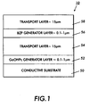
- the photoreceptor belt 10 consists of a flexible electrically conductive substrate 50.
- the substrate can be opaque, translucent, semi-transparent, or transparent, and can be of any suitable conductive material, including copper, brass, nickel, zinc, chromium, stainless steel, conductive plastics and rubbers, aluminum, semitransparent aluminum, steel, cadmium, silver, gold, paper rendered conductive by the inclusion of a suitable material therein or through conditioning in a humid atmosphere to ensure the presence of sufficient water content to render the material conductive, indium, tin, metal oxides, including tin oxide and indium tin oxide, and the like.
- the substrate can comprise an insulative layer with a conductive coating, such as vacuum-deposited metallization on plastic, such as titanized or aluminized MylarTM polyester, wherein the metalized surface is in contact with the bottom photoreceptor layer or any other layer such as a charge injection blocking or adhesive layer situated between the substrate and the bottom photoreceptor layer.
- the substrate has any effective thickness, typically from about 6 to about 250 microns, and preferably from about 50 to about 200 microns, although the thickness can be outside of this range.
- the photoreceptor belt further comprises a pair of photoreceptor structures each including a charge generation layer and a charge transport layer.
- Adhered to the substrate 50 is a first or lower generator layer 52 of GaOHPc approximately 0.1 to 1 ⁇ m thick, a first or lower transport layer 54 of N,N'-diphenyl-N,N'-bis(3''-methylphenyl)-(1,1'-biphenyl)-4,4'-diamine (TPD) in polycarbonate which is hole transporting and approximately 15 ⁇ m thick, a second or upper generator layer 56 of benzimidazole perylene (BZP) approximately 0.1 to 1 ⁇ m thick, a second or upper transport layer 58 of TPD in polycarbonate which is hole transporting and approximately 15 ⁇ m thick.
- a first or lower generator layer 52 of GaOHPc approximately 0.1 to 1 ⁇ m thick
- a first or lower transport layer 54 of N,N'-diphenyl-N,N'-bis(3''-methylphenyl)-(1,1'-biphenyl)-4,4'-diamine (TPD)
- the GaOHPc generator layer is thin enough to maintain low dark decay and the BZP generator layer is thick enough to be opaque to the wavelength used to discharge it.
- BZP is known to be coatable to opaque thicknesses while maintaining low dark decay.
- the GaOHPc generator layer is infrared sensitive at 830 nm and the BZP generator layer is red sensitive at 670 nm.
- Each generator layer can only be accessed by one of the two wavelengths.
- the BZP layer does not absorb the 830 nm wavelength and passes it to the GaOHPc layer.
- the 670 nm wavelength is absorbed by the BZP layer and is not transmitted to the GaOHPc layer (which would also be sensitive to the 670 nm light).
- the generator and transport layers can be deposited by vacuum evaporation or solvent coating upon the substrate by means known to those of ordinary skill in the art.
- the 670 nm wavelength of one modulated beam would be entirely absorbed in the opaque BZP generator layer. Exposure with the 670 nm beam would therefore discharge the BZP and upper transport layer 58. None of the 670 nm light beam would reach the GaOHPc layer so that it and the lower transport layer 54 would remain fully charged.
- the second wavelength is chosen to be 830 nm to insure that it will pass completely through the BZP layer without effecting any discharge of that layer or upper transport layer 58.
- the GaOHPc layer is sensitive to 830 nm and exposure with this wavelength from a modulated beam will discharge that layer and the lower transport layer 54. The 830 nm exposure should not be allowed to effect discharge through the benzimidazole perylene layer and the upper transport layer.
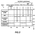
- exposure of an area of the photoreceptor belt 10 to the both wavelengths or to only one of the wavelengths results in the photoreceptor being electrostatically conditioned as follows: (a) the unexposed areas which retain the original surface voltage, (b) areas exposed with the 830nm beam which are discharged to roughly one-half of the original surface voltage, (c) areas exposed with the 670 nm beam which are also discharged to roughly one-half of the original photoreceptor voltage, V 0 and (d) the areas exposed with both the 830 nm and 670 nm wavelength beams which are fully discharged.
- the image area represented by (a) corresponds to the CAD portion of a tri-level image while the image area represented by (d) corresponds to the DAD portion of a tri-level image.
- the areas represented by (b) and (c) in Figure 2 are at a voltage level corresponding to the background level of the tri-level image. Because of the way these images were formed the area (b) represents a second DAD image area which initially is not distinguishable from the background voltage level at (c). At the appropriate point in the imaging process, the second DAD image is rendered distinguishable so that it can be developed.
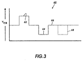
- the photoreceptor voltage profile of the photoreceptor 10 after exposure is such that it contains a tri-level image 60 comprising a charged image area 62, a discharged image area 64 and a background area 66.
- the tri-level image also includes initially a virtual image 68 which is at the same voltage level as the background voltage.
- a blue developer housing structure 80 where the CAD image 62 is developed with positively charged blue toner deposited thereon via a donor roll structure 82.
- the developer housing structure is illustrated as being a Non Interactive Development (NID) device a magnetic brush development system may also be employed since the CAD image is the first image developed.
- NID Non Interactive Development
- This development station could also employ a soft magnetic brush development system.
- the photoreceptor is uniformly recharged to the background level 66 using a corona discharge device 90 such as a scorotron or dicorotron.
- the recharge step is followed by flood exposing the entire photoreceptor 10 using an illumination source 92 operating at a suitable wavelength. The effect of this exposure step is to discharge regions of the photoreceptor containing the virtual image 68 thereby forming a second developable DAD image.
- the toners used to develop the CAD and first DAD images are opaque to light at the wavelength of the flood exposure in order to avoid developing a voltage offset after the recharge and flood exposure.
- the second developable DAD image is developed with red negatively charged toner using an NID device 93 including an electroded donor roll 94.
- the photoreceptor 10 is recharged using a corona discharge device 100. This recharge step is followed by an imagewise exposure using an infrared wavelength, e.g. 830 nm, ROS or Light Emitting Diode (LED) array 102.
- the device 102 imagewise exposes a portion of the white (undeveloped) background area 66 of the photoreceptor.
- the image formed in this manner is subsequently developed using a DAD developer system 104 including an electroded donor roll 105 which deposits negatively charged black toner on the image.
- K + 2 colors can also be achieved.
- One way for K + 2 colors to be accomplished is for the red developer device 93, , recharge device 100 and imagewise exposure device 102 to be rendered inoperative in response to a program selected by an operator using the UI 106.
- the colors as well as the black are perfectly registered because the images are all written simultaneously with the same ROS at the same imaging station. All other K+2 combinations require recharge 100 and exposure 102 be operative. In these cases only the colors are perfectly registered.
- a narrower color gamut imaging with perfectly registered RGB images is also possible.
- the recharge device 100, imagewise exposure device 102 and the black developer unit 104 are rendered inoperative.
- a tri-level image 107 is formed as the result of the imagewise exposure, step 1.
- a photoreceptor is discharged to a small but non zero potential.
- this residual voltage after full exposure is taken to be zero volts in Figure 4.
- the charge on the developed toner brings the image potential to the same level as the development bias.
- Step 2 involves developing the CAD image using blue toner where the blue developer structure is electrically biased at about 100 volts offset from the background voltage effecting deposition of positively charged blue toner on the CAD image.
- the rows of the table of Figure 4 show the charge level of the CAD, DAD and background areas of the photoreceptor at any given step in the process as well as the color toner developed on a given image area.
- Step 3 of the process effects development of the DAD image with green toner with the green developer housing bias being the offset from the background by about 100 volts in the opposite direction from the bias for the blue housing.
- the photoreceptor is recharged to mid level (step 4) and flood illuminated (step 5) in order to form the second DAD image at 0 volts (ideal situation).
- the DAD image created by the flood illumination step is then developed with negatively charged red toner, step 6.
- the bias for this development step is offset by about 100 volts from the midlevel which is the same as the offset used for the other DAD housing.
- step 5 the photoreceptor is uniformly charged to V 0 /2 (assumed here to be 400 V).
- Step 8 shows the imagewise exposure with infrared light, e.g. 830 nm, of a portion of the nondeveloped background area which creates a DAD image at residual potential, taken to be 0 volts in this case.
- Step 9 provides for development of the image created using the imagewise exposure device 102 as shown in Figure 8. This third DAD development is done with black toner with the black developer housing bias being set at about 100 volts offset from the mid level.
- a pretransfer corona discharge member 112 disposed at pretransfer charging station J is provided to condition the toner for effective transfer to a substrate using positive corona discharge.
- the pretransfer corona discharge member is preferably an AC corona device biased with a DC voltage to operate in a field sensitive mode and to perform tri-level xerography pretransfer charging in a way that selectively adds more charge (or at least comparable charge) to the part of composite tri-level image that must have its polarity reversed compared to elsewhere.
- This charge discrimination can be enhanced by discharging the photoreceptor carrying the composite developed latent image with light (not shown) before the pretransfer charging begins. Furthermore, flooding the photoreceptor with light coincident with the pretransfer charging minimizes the tendency to overcharge portions of the image which are already at the correct polarity.
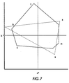
- FIGS 6A and 6B The colors achievable with RGB additive colors compared to those achievable with CMY subtractive colors are shown in Figures 6A and 6B.
- the vertical axes are designated as A for absorption, R for reflection and T for transmission of light.
- the horizontal axes show the wavelength of light and its division into spectral components.
- the CMY colors are not saturated in the RGB scheme.
- the reflection of G and R light from Y toner on paper is very high in the color-on-color CMY scheme.
- the equivalent reflection of G and R light from the color-beside-color RGB scheme is only about half the value since the R toner creates unwanted G absorption and the G toner creates unwanted R absorption.
- the CMY colors are not saturated but the RGB colors are saturated.
- the CMY colors are saturated but the RGB colors are not fully saturated due to the nature of the color pigment absorptions.
- the color gamut which can be achieved with the color on color (CMY) scheme is the area enclosed by the solid line.
- the color gamut which can be achieved with the color beside color (RGB) scheme is the area enclosed by the dashed line.
- the RGB colors in the additive scheme will generally have greater saturation than in the subtractive scheme due to the nature of the RGB color pigments.
- the color on color CMY pigments do not generally give as saturated RGB colors as the RGB pigments themselves.
- the images created using the green, blue, red and black toners, as shown in Figure 8, are transferred to a final substrate 114, such transfer taking place at transfer station K.
- Transfer station K includes a corona generating device 116 which sprays ions of a suitable polarity onto the backside of substrate 114. This attracts the charged toner powder images from the photoreceptor belt 10 to the substrate.
- a magnetic brush cleaner housing is disposed at the cleaner station L.
- the cleaner apparatus comprises a conventional magnetic brush roll structure 118 for causing carrier particles in the cleaner housing to form a brush-like orientation relative to the roll structure and the charge retentive surface. It may also include a pair of detoning rolls (not shown) for removing the residual toner from the brush. Other cleaning systems, such as fur brush or blade, are also suitable.
- a discharge lamp 113 positioned at station M floods the photoconductive surface with white light to dissipate any residual electrostatic charge remaining prior to the charging thereof for the successive imaging cycle.
- Fusing station N includes a fuser assembly, indicated generally by the reference numeral 134, which permanently affixes the transferred powder image to substrate 114.
- fuser assembly 134 comprises a heated fuser roller 136 and a backup roller 138.
- Substrate 114 passes between fuser roller 136 and backup roller 138 with the toner powder images contacting fuser roller 136. In this manner, the toner powder image is permanently affixed to substrate 114.
- a chute guides the advancing substrate 114 to a catch tray, also not shown, for subsequent removal from the printing machine by the operator.
Landscapes
- Engineering & Computer Science (AREA)
- Multimedia (AREA)
- Signal Processing (AREA)
- Physics & Mathematics (AREA)
- General Physics & Mathematics (AREA)
- Color Electrophotography (AREA)
- Color Image Communication Systems (AREA)
- Control Or Security For Electrophotography (AREA)
Applications Claiming Priority (2)
| Application Number | Priority Date | Filing Date | Title |
|---|---|---|---|
| US08/916,461 US5895738A (en) | 1997-08-22 | 1997-08-22 | Extension of xerocolorgraphy to full color printing employing additive RGB+ K colors |
| US916461 | 1997-08-22 |
Publications (3)
| Publication Number | Publication Date |
|---|---|
| EP0903643A2 true EP0903643A2 (fr) | 1999-03-24 |
| EP0903643A3 EP0903643A3 (fr) | 2000-08-30 |
| EP0903643B1 EP0903643B1 (fr) | 2003-06-11 |
Family
ID=25437306
Family Applications (1)
| Application Number | Title | Priority Date | Filing Date |
|---|---|---|---|
| EP98115354A Expired - Lifetime EP0903643B1 (fr) | 1997-08-22 | 1998-08-14 | Système d'impression xérographique en toutes couleurs |
Country Status (4)
| Country | Link |
|---|---|
| US (1) | US5895738A (fr) |
| EP (1) | EP0903643B1 (fr) |
| JP (1) | JPH11109705A (fr) |
| DE (1) | DE69815459T2 (fr) |
Cited By (2)
| Publication number | Priority date | Publication date | Assignee | Title |
|---|---|---|---|---|
| EP0921443A3 (fr) * | 1997-11-24 | 2000-05-17 | Xerox Corporation | Impression électrophotographique en couleur avec rechargement, exposition et développement additif |
| US7126621B2 (en) | 2004-07-30 | 2006-10-24 | Xerox Corporation | Printer using hybrid reflex writing to color register an image |
Families Citing this family (9)
| Publication number | Priority date | Publication date | Assignee | Title |
|---|---|---|---|---|
| JP3598209B2 (ja) * | 1997-12-05 | 2004-12-08 | コニカミノルタビジネステクノロジーズ株式会社 | 画像形成装置 |
| GB2338075B (en) | 1998-03-24 | 2001-12-12 | Hewlett Packard Co | Color plane under exposure for reducing edge effect |
| US6203953B1 (en) | 1999-11-10 | 2001-03-20 | Xerox Corporation | Method for forming a toner image with low toner pile height |
| US6937362B1 (en) * | 2000-04-05 | 2005-08-30 | Eastman Kodak Company | Method for providing access to an extended color gamut digital image and providing payment therefor |
| US20030035138A1 (en) * | 2001-08-17 | 2003-02-20 | Schilling Mary K. | Internet-based custom package-printing process |
| US7734225B2 (en) * | 2007-03-28 | 2010-06-08 | Xerox Corporation | Tri-level tandem xerographic architecture using reduced strength toner |
| US8007969B2 (en) * | 2008-06-09 | 2011-08-30 | Xerox Corporation | Tri-level xerography for hypochromatic colorants |
| US10180649B2 (en) * | 2015-12-04 | 2019-01-15 | Xerox Corporation | Systems and methods for implementing electrophotographic layered manufacturing of three dimensional (3D) objects, parts and components using tri-level electrophotography |
| DE102016109044B3 (de) | 2016-05-17 | 2017-07-06 | Leonhard Kurz Stiftung & Co. Kg | Vorrichtung zur Oberflächenbehandlung eines Substrats |
Family Cites Families (15)
| Publication number | Priority date | Publication date | Assignee | Title |
|---|---|---|---|---|
| US4731634A (en) * | 1986-11-03 | 1988-03-15 | Xerox Corporation | Apparatus for printing black and plural highlight color images in a single pass |
| US4868611A (en) * | 1987-12-10 | 1989-09-19 | Xerox Corporation | Highlight color imaging with first image neutralization using a scorotron |
| US5049949A (en) * | 1989-06-29 | 1991-09-17 | Xerox Corporation | Extension of tri-level xerography to black plus 2 colors |
| US5155541A (en) * | 1991-07-26 | 1992-10-13 | Xerox Corporation | Single pass digital printer with black, white and 2-color capability |
| US5223906A (en) * | 1992-08-03 | 1993-06-29 | Xerox Corporation | Four color toner single pass color printing system using two tri-level xerographic units |
| US5221954A (en) * | 1992-10-01 | 1993-06-22 | Xerox Corporation | Single pass full color printing system using a quad-level xerographic unit |
| US5337136A (en) * | 1992-10-23 | 1994-08-09 | Xerox Corporation | Tandem trilevel process color printer |
| JPH07301968A (ja) * | 1992-12-07 | 1995-11-14 | Xerox Corp | カラー画像形成方法及び画像形成装置 |
| US5373313A (en) * | 1992-12-09 | 1994-12-13 | Xerox Corporation | Color xerographic printing system with multiple wavelength, single optical system ROS and multiple layer photoreceptor |
| US5444463A (en) * | 1992-12-09 | 1995-08-22 | Xerox Corporation | Color xerographic printing system with dual wavelength, single optical system ROS and dual layer photoreceptor |
| US5347303A (en) * | 1993-01-04 | 1994-09-13 | Xerox Corporation | Full color xerographic printing system with dual wavelength, single optical system ROS and dual layer photoreceptor |
| US5592281A (en) * | 1994-11-25 | 1997-01-07 | Xerox Corporation | Development scheme for three color highlight color trilevel xerography |
| US5534990A (en) * | 1995-03-31 | 1996-07-09 | Xerox Corporation | Full color printing system using a penta-level xerographic unit |
| US5565974A (en) * | 1995-03-31 | 1996-10-15 | Xerox Corporation | Penta-level xerographic unit |
| US5716744A (en) * | 1996-03-05 | 1998-02-10 | Hewlett-Packard Company | Dual beam color electrophotographic apparatus |
-
1997
- 1997-08-22 US US08/916,461 patent/US5895738A/en not_active Expired - Lifetime
-
1998
- 1998-08-10 JP JP10225757A patent/JPH11109705A/ja not_active Withdrawn
- 1998-08-14 DE DE69815459T patent/DE69815459T2/de not_active Expired - Fee Related
- 1998-08-14 EP EP98115354A patent/EP0903643B1/fr not_active Expired - Lifetime
Cited By (2)
| Publication number | Priority date | Publication date | Assignee | Title |
|---|---|---|---|---|
| EP0921443A3 (fr) * | 1997-11-24 | 2000-05-17 | Xerox Corporation | Impression électrophotographique en couleur avec rechargement, exposition et développement additif |
| US7126621B2 (en) | 2004-07-30 | 2006-10-24 | Xerox Corporation | Printer using hybrid reflex writing to color register an image |
Also Published As
| Publication number | Publication date |
|---|---|
| DE69815459T2 (de) | 2004-01-15 |
| DE69815459D1 (de) | 2003-07-17 |
| EP0903643A3 (fr) | 2000-08-30 |
| US5895738A (en) | 1999-04-20 |
| JPH11109705A (ja) | 1999-04-23 |
| EP0903643B1 (fr) | 2003-06-11 |
Similar Documents
| Publication | Publication Date | Title |
|---|---|---|
| EP0898208B1 (fr) | Système d'impression xérographique | |
| EP0606141B1 (fr) | Copier électrophotographique en couleurs à ROS et photorécepteur à deux couches | |
| US4515462A (en) | Method and apparatus for forming multicolor image | |
| US5373313A (en) | Color xerographic printing system with multiple wavelength, single optical system ROS and multiple layer photoreceptor | |
| US5223906A (en) | Four color toner single pass color printing system using two tri-level xerographic units | |
| EP0903643B1 (fr) | Système d'impression xérographique en toutes couleurs | |
| US4961094A (en) | Electrostatic recording apparatus and method for producing color images | |
| US5807652A (en) | Process for producing process color in a single pass with three wavelength imager and three layer photoreceptor | |
| US5444463A (en) | Color xerographic printing system with dual wavelength, single optical system ROS and dual layer photoreceptor | |
| US5751437A (en) | Development combination exposure and recharge scheme to eliminate development defects in two pass process color xerocolography | |
| US6133933A (en) | Color Xerographic printing system with multicolor printbar | |
| US5592281A (en) | Development scheme for three color highlight color trilevel xerography | |
| US6028616A (en) | Enhanced color gamut from 2-pass xerocolography with 2λ imager and 2-layer photoreceptor | |
| EP0601758B1 (fr) | Système d'impression xérographique en couleur avec des longeurs d'onde multiples, système optique unique et photorécepteur multicouche | |
| EP0735433B1 (fr) | Unité xérographique à cinq niveaux | |
| US5790928A (en) | Switchable dual wavelength flood lamp for simplified color printing architecture based on xerocolography | |
| EP0088553B1 (fr) | Procédé et appareil pour la formation d'images à couleurs multiples | |
| JPS60237467A (ja) | 画像形成方法 | |
| JPH03296779A (ja) | 画像形成方法 | |
| JPS62296173A (ja) | 色分解機能を有する感光体を用いた変倍可能複写機 | |
| JPH05107862A (ja) | フルカラー画像形成方法及びその装置 | |
| JPH03296778A (ja) | 画像形成方法 | |
| JPS62296170A (ja) | 色分解機能を有する感光体を用いた画像形成装置 | |
| JPH01193762A (ja) | 画像形成装置 | |
| JPH05150608A (ja) | フルカラー画像形成方法 |
Legal Events
| Date | Code | Title | Description |
|---|---|---|---|
| PUAI | Public reference made under article 153(3) epc to a published international application that has entered the european phase |
Free format text: ORIGINAL CODE: 0009012 |
|
| AK | Designated contracting states |
Kind code of ref document: A2 Designated state(s): DE FR GB |
|
| AX | Request for extension of the european patent |
Free format text: AL;LT;LV;MK;RO;SI |
|
| PUAL | Search report despatched |
Free format text: ORIGINAL CODE: 0009013 |
|
| AK | Designated contracting states |
Kind code of ref document: A3 Designated state(s): AT BE CH CY DE DK ES FI FR GB GR IE IT LI LU MC NL PT SE |
|
| AX | Request for extension of the european patent |
Free format text: AL;LT;LV;MK;RO;SI |
|
| 17P | Request for examination filed |
Effective date: 20010228 |
|
| AKX | Designation fees paid |
Free format text: DE FR GB |
|
| 17Q | First examination report despatched |
Effective date: 20010424 |
|
| GRAH | Despatch of communication of intention to grant a patent |
Free format text: ORIGINAL CODE: EPIDOS IGRA |
|
| GRAH | Despatch of communication of intention to grant a patent |
Free format text: ORIGINAL CODE: EPIDOS IGRA |
|
| GRAA | (expected) grant |
Free format text: ORIGINAL CODE: 0009210 |
|
| AK | Designated contracting states |
Designated state(s): DE FR GB |
|
| REG | Reference to a national code |
Ref country code: GB Ref legal event code: FG4D |
|
| REF | Corresponds to: |
Ref document number: 69815459 Country of ref document: DE Date of ref document: 20030717 Kind code of ref document: P |
|
| ET | Fr: translation filed | ||
| PLBE | No opposition filed within time limit |
Free format text: ORIGINAL CODE: 0009261 |
|
| STAA | Information on the status of an ep patent application or granted ep patent |
Free format text: STATUS: NO OPPOSITION FILED WITHIN TIME LIMIT |
|
| 26N | No opposition filed |
Effective date: 20040312 |
|
| REG | Reference to a national code |
Ref country code: GB Ref legal event code: 746 Effective date: 20040910 |
|
| REG | Reference to a national code |
Ref country code: FR Ref legal event code: D6 |
|
| PGFP | Annual fee paid to national office [announced via postgrant information from national office to epo] |
Ref country code: FR Payment date: 20060808 Year of fee payment: 9 |
|
| PGFP | Annual fee paid to national office [announced via postgrant information from national office to epo] |
Ref country code: GB Payment date: 20060809 Year of fee payment: 9 |
|
| PGFP | Annual fee paid to national office [announced via postgrant information from national office to epo] |
Ref country code: DE Payment date: 20060810 Year of fee payment: 9 |
|
| GBPC | Gb: european patent ceased through non-payment of renewal fee |
Effective date: 20070814 |
|
| REG | Reference to a national code |
Ref country code: FR Ref legal event code: ST Effective date: 20080430 |
|
| PG25 | Lapsed in a contracting state [announced via postgrant information from national office to epo] |
Ref country code: DE Free format text: LAPSE BECAUSE OF NON-PAYMENT OF DUE FEES Effective date: 20080301 |
|
| PG25 | Lapsed in a contracting state [announced via postgrant information from national office to epo] |
Ref country code: FR Free format text: LAPSE BECAUSE OF NON-PAYMENT OF DUE FEES Effective date: 20070831 |
|
| PG25 | Lapsed in a contracting state [announced via postgrant information from national office to epo] |
Ref country code: GB Free format text: LAPSE BECAUSE OF NON-PAYMENT OF DUE FEES Effective date: 20070814 |