EP0903650A1 - Minuterie avec compteur de temps - Google Patents
Minuterie avec compteur de temps Download PDFInfo
- Publication number
- EP0903650A1 EP0903650A1 EP98117738A EP98117738A EP0903650A1 EP 0903650 A1 EP0903650 A1 EP 0903650A1 EP 98117738 A EP98117738 A EP 98117738A EP 98117738 A EP98117738 A EP 98117738A EP 0903650 A1 EP0903650 A1 EP 0903650A1
- Authority
- EP
- European Patent Office
- Prior art keywords
- value
- counter
- timer
- key
- timer device
- Prior art date
- Legal status (The legal status is an assumption and is not a legal conclusion. Google has not performed a legal analysis and makes no representation as to the accuracy of the status listed.)
- Granted
Links
Images


Classifications
-
- G—PHYSICS
- G04—HOROLOGY
- G04F—TIME-INTERVAL MEASURING
- G04F1/00—Apparatus which can be set and started to measure-off predetermined or adjustably-fixed time intervals without driving mechanisms, e.g. egg timers
- G04F1/005—Apparatus which can be set and started to measure-off predetermined or adjustably-fixed time intervals without driving mechanisms, e.g. egg timers using electronic timing, e.g. counting means
-
- G—PHYSICS
- G06—COMPUTING OR CALCULATING; COUNTING
- G06F—ELECTRIC DIGITAL DATA PROCESSING
- G06F1/00—Details not covered by groups G06F3/00 - G06F13/00 and G06F21/00
- G06F1/04—Generating or distributing clock signals or signals derived directly therefrom
- G06F1/06—Clock generators producing several clock signals
Definitions
- the present invention relates to a timer device, and more particularly, to a timer device having a timer counter.
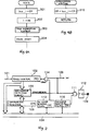
- Fig. 7 is a block diagram showing one example of a conventional timer device.
- a timer counter (TC) 102 is counted up by a count clock signal 101.
- a comparison register (CR) 103 is connected to a bus(104) and is used for setting a coincidence signal time.
- a coincidence detecting circuit 105 compares the value of the timer counter (TC) 102 with that of the comparison register (CR) 103 to produce a coincidence signal 106 when both values agree with each other.
- a clock latch 108 (D flip flop) outputs the value of an output value setting bit (OD) 107 to an output terminal 109 for every output of the coincidence signal 106. Further, data reading and data writing with respect to the comparison register (CR) 103 and the output value setting bit (OD) 107 are carried out through the bus 104.
- a timer device 401 is connected through a bus 404 (equivalent to the bus 104 in Fig. 7) to a random access memory (RAM) 402 and a central processing unit (CPU) 403, and is also connected to a buzzer 405.
- a key 406 is also connected to the bus 404.
- the CPU 403 provides a key counter (key) and a buzzer counter (buz) to the RAM 402.
- a key counter key
- a buzzer counter buz
- the initial value key_i of key interruption interval time and the initial value buz_i of terminal reverse interval time are assigned in the key counter (key) and the buzzer counter (buz) (Steps 201, 202).
- the value of the key counter (key) is compared with that of the buzzer counter (buz) (Step 203).
- the value of the key counter (key) is assigned through the bus 104 in the comparison register (CR) 103 shown in Fig. 7 in the timer device 401 (Step 204).
- the value of the buzzer counter (buz) is assigned through the bus 104 in the comparison register (CR) 103 (Step 205).
- the CPU 403 enables the interruption of the timer device 401 (Step 206) to start the timer device 401 (Step 207).
- Step 211 comparison is made to see whether or not the value of the key counter (key) shown is below that of the timer counter (TC) 102 (Step 211). If the value of the key counter (key) is below that of the timer counter (TC) 102, key interruption interval time key_i is added to the value of the key counter (key) to renew the value of the key counter (key) (Step 212).
- Step 213 comparison is made to see whether or not the value of the buzzer counter (buz) is below the value of the timer counter (TC) 102 (Step 213). If the value of the buzzer counter (buz) is below that of the timer counter (TC) 102, terminal inverse interval time buz_i is added to the value of the buzzer counter (buz) to renew the value of the buzzer counter (buz) (Step 214).
- Step 215 the value of the key counter (key) is compared with that of the buzzer counter (buz) (Step 215).
- the value of the buzzer counter (buz) is below that of the key counter (key)
- the value of the buzzer counter (buz) is substituted in the comparison register (CR) 103 (Step 219).
- the initial value 1100 H is set to the key counter (key) (Step 201).
- the initial value 600 H is set to the buzzer counter (buz) (Step 202).
- the value (600 H) of the buzzer counter (buz) is lower than the value (1100 H) of the key counter (key). Accordingly, the value (600 H) of the buzzer counter (buzz) is substituted for the comparison register (CR) 103 (Steps 203 and 205).
- timer interruption is enabled to start the timer (Steps 206 and 207).
- the output value setting bit (OD) 107 is inverted (Steps 216, 217 or 218) to assign the value (C00 H) of the buzzer counter (buz) in the comparison register (CR) 103 (Step 219), terminating the interruption processing.
- the value (C00 H) of the timer counter (TC) 102 is equal to the value (C00 H) of the buzzer counter (buz).
- the value of the buzzer counter (buz) yields 1200 H (Steps 213, 214).
- comparison of the value (1100 H) of the key counter (key) with the added value (1200 H) of the buzzer counter (buz) discloses that the value of the key counter (key) is lower than that of the buzzer counter (buz).
- the value (1100 H) of the key counter (key) is substituted in the comparison register (CR) 103, terminating the interruption processing (output value setting bit (OD) 107 is not allowed to inverse).
- this software inverses the output of the output terminal 109 for every 600 H of the timer counter (TC) 102 to sound a buzzer 405 in Fig. 11, carrying out data fetching processing for a key 406 for every 1100 H of the timer counter (TC) 102.
- the main program in Fig. 10 A substitute buz_i for the comparison register (CR) 103 (Step 301) to enable the interruption of the timer device (Step 303), starting the timer (Step 304).
- the interruption routine shown in Fig. 10B and activated in the CPU for every output of the coincidence signal from the timer device the output value setting bit (OD) 107 is inverted (Steps 321, 322 or 323).
- Buz_i is then added to the comparison register (CR) 103.
- the added buz_i is set as a new value of the comparison register (CR) through the bus 404 (104) (Step 324).
- the conventional timer device described above requires for setting (for example, step 216 to 218 of Fig. 8B) of the output value setting bit (OD) 107 by the interruption process when the timer device is used for the inverse output off the output terminal 109. This prolongs software processing duration and result in problems access timing becomes tight.
- Another object of the present invention is to design software timing problem-free, and to provide a timer device capable of reducing the time period of test by the use for the designed software.
- a timer device of the present invention comprises: a timer counter for counting count clocks; a register; a coincidence detecting circuit for producing a coincidence signal when value stored in the register with value of the timer counter; a reverse enable flag which is set a flag; a signal generating circuit for reversing an output signal output to an output terminal when the flag indicates a value corresponding to inverse enabling and the coincidence signal is generated from the coincidence detecting circuit.
- the timer device is configured to inverse the output signal output to the output terminal when the inverse enable flag has the value showing inverse enabling and also when the coincidence signal is generated from the coincidence detecting circuit. Accordingly, an arithmetic unit connected to the timer device requires no software process for detecting the value of the output value setting bit (OD) and reversing the value of the output value setting bit (OD) in accordance with the detected value unlike conventional timer devices for latching the value of the output value setting bit (OD) by the coincidence signal to obtain an output signal.
- Fig. 1 is a block diagram of a timer device according to a first embodiment of the present invention.
- a timer counter (TC) 102 is counted up by count clocks 101.
- a comparison register (CR) 103 is set to a number necessary for coincidence time as described later.
- a coincidence detecting circuit 105 compares the value of the timer counter (TC) 102 with that of the comparison register (CR) 103 to produce a coincidence signal 106 when both the values agree with each other.
- An AND circuit 111 as a logic circuit receives value of an inverse (reverse) enable (permission) flag (RE) 110 and a coincidence signal 106.
- a T-type flip-flop (T-F/F) 112 receives the output signal of the AND circuit 111 to a trigger input terminal T thereof to reverse its output signal (logic level, for example, "1" or "0") output to an output terminal 109.
- a CPU (not shown) carries out data reading and data writing with respect to the comparison register (CR) 103 and the inverse enable flag (RE) 110 through a bus 104.
- the count value of the timer counter (TC) 102 is output through the bus 104 to the CPU (not shown).
- FIG. 2A the same reference numerals as those in Figs. 8A and 8B are employed in the same process steps.
- a key counter (key) and a buzzer counter (buz) are provided in a RAM 402 in Fig. 11.
- a main (MAIN) program carried out by the CPU 403 in Fig. 11 substitutes the initial value key_i of key interruption interval time and the initial value buz_i of terminal inverse interval time for the key counter (key) and the buzzer counter (buz) (Steps 201 and 202).
- the CPU 403 compares the value of the key counter (key) with that of the buzzer counter (buz) (Step 203).
- the value of the key counter (key) is supplied through the bus 404 (104) to the comparison register (CR) 103 in the timer device 401 (Step 204).
- the value of the buzzer counter (buz) is supplied through the bus 404 (104) to the comparison register (CR) 103 (step 205).
- Interruption of the timer device is then enabled (Step 206) to start the timer device 401 having a construction shown in Fig. 1 (Step 207).
- the value of the timer counter (TC) 102 is counted up for every input of clock pluse of signal 101.
- the coincidence detecting circuit 105 detects coincidence of the counted value with the set value of the comparison register (CR) 103, a coincidence signal 106 is output from the coincidence detecting circuit 105 when the two inputs are coincident.
- the coincidence signal 106 as an interruption signal is input to the CPU 403 in Fig. 11.
- the CPU 403 starts an interruption routine shown in Fig. 2B.
- the value of the timer counter (TC) 102 is compared with that of the key counter (key) (Step 211).
- the value of the key counter (key) is added and renewed by key_i (Step 212).
- Step 212 the value of the timer counter (TC) 102 is compared with that of the buzzer counter (buz) (Step 213).
- the value of the buzzer counter (buz) is added and renewed by buz_i (Step 214).
- Step 214 the value of the timer counter (TC) 102 is lower than that of the buzzer counter (buz) in Step 213, the value of the key counter (key) is then compared with that of the buzzer counter (buz) (Step 215).
- the comparison result discloses that the value of the buzzer counter (buz) is below that of the key counter (key)
- the CPU 403 substitutes "1" through the bus 404 (104) for the inverse enable flag (RE) 110 in Fig. 1 (Step 221), and also substitutes the value of the buzzer counter (buz) for the comparison register (CR) 103 (Step 222).
- Step 215 when the comparison result discloses that the value of the buzzer counter (buz) is higher than that of the key counter (key), the CPU 403 substitutes "0" through the bus 404 (104) for the inverse enable flag (RE) 110 in Fig. 1 (Step 223), and also substitutes the value of the key counter (key) for the comparison register (CR) 103 (Step 224).
- Fig. 3 shows a change in each value of the timer counter 102, the buzzer counter (buz), the key counter (key), and the comparison register (CR) 103, a change in each signal of the coincidence signal 106, the inverse enable flag (RE) 110, and the output terminal (TO) 109, and the timing of the key interruption processing.
- Fig. 3 shows an example that the terminal inverse interval time buz_i yields 600 H, the key interruption interval time key_i yields 1100 H as explained below.
- the CPU 403 sets the initial value 1100 H to the key counter (key) (Step 201) and sets the initial value 600 H to the buzzer counter (buz) (Step 202) in accordance with the main program in Fig. 2A.
- the value of the key counter (key) is compared with that of the buzzer counter (buz) in their magnitudes (Step 203). In this case, the value (600 H) of the buzzer counter (buz) is lower than the value (1100 H) of the key counter (key).
- the CPU 403 sets the value (600 H) of the buzzer counter (biz) to the comparison register (CR) 103 in Fig. 1 (Step 205). Timer interruption is then enabled (Step 206) to start the timer (Step 207).
- the above operation starts the counting of the counter clocks 101 by using the timer counter (TC) 102.
- the coincidence signal 106 is output from the coincidence detecting circuit 105 to apply the coincidence signal 106 to the AND circuit 111.
- the inverse enable flag (RE) 110 is supposed to be set to "1," the above coincidence signal 106 is applied through the AND circuit 111 to the trigger terminal of the T-F/F 112 to inverse the output (The output signal from the output terminal 109 comes to high level as shown in Fig. 3, for example.).
- the above coincidence signal 106 as the interruption signal is input to the CPU 403 in Fig. 11 to start the interruption routine shown in Fig. 2B.
- the value of the timer counter (TC) 102 is the same as the value (600 H) of the comparison register (CR) 103, namely, the initial value (600 H) of the buzzer counter (buz).
- the interruption routine renews the value C00 H obtained by adding the initial value buz_i (600 H) to the value of the buzzer counter (buz) as the value of the buzzer counter (buz) (Steps 211 to 214).
- the CPU 403 substitutes "1" through the bus 404 (104) for the inverse enable flag (RE) 110 (Steps 215 and 221), and also substitutes the value (C00 H) of the buzzer counter (buz) for the comparison register (CR) 103 (Step 222) and terminates the interruption process.
- the inverse enable flag 110 changes "1,"
- the AND circuit 111 in Fig. 1 is in an "through” gate state. That is, the AND circuit 111 is ready to output its output signal having a high logic level when a value of the timer counter 120 becomes C00 H and a coincidence signal is generated at that time. It is noted that when the inverse enable flag 110 is set to "1", the coincidence signal 106 has not yet been again generated (see waveforms of coincidence signal 100 and revcerse enable flag 110 in Fig. 3).
- the timer counter (TC) 102 continues counting. Again, when the value (C00 H) of the comparison register (CR) 103 equalizes to the value of the timer counter (TC) 102, the coincidence signal 106 is output from the coincidence detecting circuit 105. The coincidence signal 106 triggers through the AND circuit 111 the T-F/F 112 to inverse the Q output signal of the T-F/F 112 output to the output terminal 109 to low level, for example.
- the CPU 403 starts the interruption routine shown in Fig. 2B by using the above coincidence signal 106.
- the interruption routine renews the value 1200 H obtained by adding the initial value buz_i (600 H) to the value of the buzzer counter (buz) as the value of the buzzer counter (buz) (Steps 211 to 214).
- the CPU 403 substitutes "0" through the bus 404 (104) for the inverse enable flag (RE) 110 (Steps 215, 223) and also substitutes the value (1100 H) of the key counter (key) for the comparison register (CR) 103 (Step 224) and terminates the interruption process.
- the inverse enable flag 110 is "0,”
- the AND circuit 111 is in a "no-through” gate state. That is, the AND cirucit 111 outputs its output signal having a low logic level regardless of the output of the coincidence detecting circuit.
- the timer counter (TC) 102 continues counting. Again, when the value (1100 H) of the comparison register (CR) 103 equalizes to the value of the timer counter (TC) 102, the coincidence signal 106 is output from the coincidence detecting circuit 105. The coincidence signal 106 is inhibited by the AND circuit 111 from transmission to the trigger terminal T of the T-F/F 112. As a result, output signal from the output terminal 109 is not inverted.
- the CPU 403 starts the interruption routine shown in Fig. 2B by using the above coincidence signal 106.
- the value of the timer counter (TC) 102 is the same as the value (1100 H) of the key counter (key). Accordingly, the interruption routine renews the value 2200 H obtained by adding the initial value key_i (1100 H) to the value of the key counter (key) as the value of the key counter (key) (Steps 211 and 212).
- the CPU 403 substitutes "1" through the bus 404 (104) for the inverse enable flag (RE) 110 (Steps 215, 221) and also substitutes the value (1200 H) of the buzzer counter (buz) for the comparison register (CR) 103 (Step 222) to terminate the interruption process.
- the inverse enable flag 110 is "1,” the AND circuit 111 is in an "through” gate state. That is, the AND circuit 111 is ready to output its output signal having a high logic level when a value of the timer counter 120 becomes 1200 H and a coincidence signal is generated at that time.
- the timer counter (TC) 102 continues counting. Again, when the value (1200 H) of the comparison register (CR) 103 equalizes to the value of the timer counter (TC) 102, the coincidence signal 106 is output from the coincidence detecting circuit 105. The coincidence signal 106 triggers through the AND circuit 111 the T-F/F 112. As a result, the output signal Q of the T-F/F 112 output to the output terminal 109 is inverted to high level, for example.
- the CPU 403 starts the interruption routine shown in Fig. 2B by using the above coincidence signal 106.
- the value of the timer counter (TC) 102 is the same as the value (1200 H) of the buzzer counter (buz).
- the interruption routine renews the value 1800 H obtained by adding the initial value buz_i (600 H) to the value (1200 H) of the buzzer counter (buz) as the value of the buzzer counter (buz) (steps 211 to 214).
- the CPU 403 substitutes "1" through the bus 404 (104) for the inverse enable flag (RE) 110 (steps 215 and 221) and also substitutes the value (1200 H) of the buzzer counter (buz) for the comparison register (CR) 103 (Step 222) to terminate the interruption process.
- the inverse enable flag 110 is "1,” the AND circuit 111 is in an "through” gate state. That is, the AND circuit 111 is ready to output its output signal having a high logic level when a value of the timer counter 120 becomes 1800 H and a coincidence signal is generated at that time.
- the number of steps passing through the first path consisting of Steps 211 to 215, 221, and 222 in Fig. 2B is "6.”
- the number of steps passing through the second path consisting of Steps 211 to 215, 223, and 224 is also "6.”
- Figs. 4A and 4B the same reference numerals as those in Fig. 10 are employed in the same process steps.
- the main program shown in Fig. 4A buz_i is substituted for the comparison register (CR) 103 (Step 301). "1" is then substituted for the inverse enable flag (RE) 110 in Fig. 1 (Step 302).
- the interruption of the timer device is then enabled (Step 303) to start the timer (Step 304).
- buz_i is added to the comparison register (CR) 103 (Step 310) to terminate the interruption process.
- the output signal from the output terminal 109 is inverted for every stepping of the value of the timer counter (TC) 102 by the value of buz_i.
- this timer device provides a clear enable flag (CE) 113 capable of writing and reading through the bus 104.
- the timer counter (TC) 102 is cleared by the output signal from an AND circuit 114 applying AND operation to the clear enable flag (CE) 113 and the coincidence signal 106.
- the coincidence signal 106 is output from the coincidence detecting circuit 105.
- the coincidence signal 106 is then supplied through the AND circuit 111 to the trigger terminal of the T-F/F 112 to thereby inverse the output signal Q of the T-F/F 111 output to the output terminal 109, and simultaneously clears through the AND circuit 114 the timer counter (TC) 102 by the coincidence signal 106. This operation is repeated for every stepping of the value of the timer counter (TC) 102 to the comparison register (CR) 103 by the value of the terminal inverse interval time buz-i.
- the output signal from the output terminal 109 is inverted for every terminal inverse interval time buz_i.
- the output signal-supplied buzzer 405 in Fig. 11 may be buzzed.
- interruption routine of the CPU since interruption routine of the CPU is not required, further simplification of the software and reduction of the execution time may be made.
- the timer device has the inverse enable flag for enabling or inhibiting inversion.
- the arithmetic unit connected to the timer device eliminates the need for the software process for detecting the value of the output value setting bit (OD) and for inverting the value of the output value setting bit (OD) based on the detected value.
- efficient operation of software is obtained even when the software is used as an absolute time timer for the terminal output process and the internal process, and even when the software is used as the terminal output process only, thereby reducing processing time, and realizing cost reduction.
- the timer device of the present invention when the timer counter is cleared for every coincidence signal input, and the inverse enable flag has the value showing inverse enabling, and also when the coincidence detecting circuit outputs the coincidence signal, the value of the register for comparing with the value of the timer counter is fixed to a given value by inverting the output signal to the output terminal.
Landscapes
- Physics & Mathematics (AREA)
- Engineering & Computer Science (AREA)
- General Physics & Mathematics (AREA)
- Theoretical Computer Science (AREA)
- General Engineering & Computer Science (AREA)
- Programmable Controllers (AREA)
- Stabilization Of Oscillater, Synchronisation, Frequency Synthesizers (AREA)
- Measurement Of Predetermined Time Intervals (AREA)
- Input From Keyboards Or The Like (AREA)
- Measurement Of Unknown Time Intervals (AREA)
Applications Claiming Priority (3)
| Application Number | Priority Date | Filing Date | Title |
|---|---|---|---|
| JP09255310A JP3082721B2 (ja) | 1997-09-19 | 1997-09-19 | タイマ装置 |
| JP255310/97 | 1997-09-19 | ||
| JP25531097 | 1997-09-19 |
Publications (2)
| Publication Number | Publication Date |
|---|---|
| EP0903650A1 true EP0903650A1 (fr) | 1999-03-24 |
| EP0903650B1 EP0903650B1 (fr) | 2002-04-10 |
Family
ID=17277009
Family Applications (1)
| Application Number | Title | Priority Date | Filing Date |
|---|---|---|---|
| EP98117738A Expired - Lifetime EP0903650B1 (fr) | 1997-09-19 | 1998-09-18 | Minuterie avec compteur de temps, registre et circuit détecteur de coincidence ainsi que procédé de contrôle d'une sortie de circuit à l'aide d'une telle minuterie |
Country Status (6)
| Country | Link |
|---|---|
| US (1) | US6046965A (fr) |
| EP (1) | EP0903650B1 (fr) |
| JP (1) | JP3082721B2 (fr) |
| KR (1) | KR100316419B1 (fr) |
| CN (1) | CN1139858C (fr) |
| DE (1) | DE69804733T2 (fr) |
Families Citing this family (6)
| Publication number | Priority date | Publication date | Assignee | Title |
|---|---|---|---|---|
| JP4111636B2 (ja) * | 1999-08-20 | 2008-07-02 | 富士通株式会社 | 周期補正分周回路及びこれを用いた周期補正型発振回路 |
| CN101151584B (zh) * | 2005-03-31 | 2010-12-08 | 日本电气株式会社 | 定时器电路及使用定时器电路的移动通信终端和电子设备 |
| JP4501823B2 (ja) * | 2005-09-14 | 2010-07-14 | 日本電気株式会社 | 割り込み信号制御装置、割り込み信号制御方法及び割り込み信号制御プログラム |
| FR2895101A1 (fr) * | 2005-12-16 | 2007-06-22 | St Microelectronics Sa | Dispositif multifonctionnel temporisateur/compteur d'evenements et procede de mise en oeuvre d'un tel dispositif. |
| JP4780098B2 (ja) * | 2007-12-13 | 2011-09-28 | 株式会社デンソー | マイクロコンピュータ |
| TWI588696B (zh) * | 2015-08-19 | 2017-06-21 | 遠翔科技股份有限公司 | 觸控校正系統及觸控校正方法 |
Citations (3)
| Publication number | Priority date | Publication date | Assignee | Title |
|---|---|---|---|---|
| US4805199A (en) * | 1987-09-14 | 1989-02-14 | Mitsubishi Denki Kabushiki Kaisha | Pulse generating circuit |
| EP0369963A2 (fr) * | 1988-11-17 | 1990-05-23 | International Business Machines Corporation | Circuit rythmeur |
| DE4204730A1 (de) * | 1992-02-17 | 1994-03-03 | Siemens Ag | Verfahren und Schaltungsanordnung zur Erzeugung von Taktsignalen für mehrere Taktverbraucher aus einem Systemtakt |
-
1997
- 1997-09-19 JP JP09255310A patent/JP3082721B2/ja not_active Expired - Fee Related
-
1998
- 1998-09-18 EP EP98117738A patent/EP0903650B1/fr not_active Expired - Lifetime
- 1998-09-18 CN CNB981200087A patent/CN1139858C/zh not_active Expired - Fee Related
- 1998-09-18 KR KR1019980038709A patent/KR100316419B1/ko not_active Expired - Fee Related
- 1998-09-18 DE DE69804733T patent/DE69804733T2/de not_active Expired - Fee Related
- 1998-09-21 US US09/157,534 patent/US6046965A/en not_active Expired - Lifetime
Patent Citations (3)
| Publication number | Priority date | Publication date | Assignee | Title |
|---|---|---|---|---|
| US4805199A (en) * | 1987-09-14 | 1989-02-14 | Mitsubishi Denki Kabushiki Kaisha | Pulse generating circuit |
| EP0369963A2 (fr) * | 1988-11-17 | 1990-05-23 | International Business Machines Corporation | Circuit rythmeur |
| DE4204730A1 (de) * | 1992-02-17 | 1994-03-03 | Siemens Ag | Verfahren und Schaltungsanordnung zur Erzeugung von Taktsignalen für mehrere Taktverbraucher aus einem Systemtakt |
Non-Patent Citations (2)
| Title |
|---|
| "HARDWARE SUPPORT FOR AN OPERATING SYSTEM TIMER", IBM TECHNICAL DISCLOSURE BULLETIN, vol. 34, no. 10B, 1 March 1992 (1992-03-01), pages 237 - 238, XP000302701 * |
| "SIMULATION OF MULTIPLE TIMERS USING ONE ACTUAL TIMER", IBM TECHNICAL DISCLOSURE BULLETIN, vol. 38, no. 3, 1 March 1995 (1995-03-01), pages 301 - 303, XP000508059 * |
Also Published As
| Publication number | Publication date |
|---|---|
| DE69804733D1 (de) | 2002-05-16 |
| KR19990029943A (ko) | 1999-04-26 |
| CN1139858C (zh) | 2004-02-25 |
| US6046965A (en) | 2000-04-04 |
| CN1218211A (zh) | 1999-06-02 |
| JP3082721B2 (ja) | 2000-08-28 |
| JPH1195864A (ja) | 1999-04-09 |
| EP0903650B1 (fr) | 2002-04-10 |
| DE69804733T2 (de) | 2002-10-24 |
| KR100316419B1 (ko) | 2002-01-16 |
Similar Documents
| Publication | Publication Date | Title |
|---|---|---|
| EP0238090B1 (fr) | Micro-ordinateur capable d'accéder à une mémoire interne à un temps d'accès variable désiré | |
| US6457148B1 (en) | Apparatus for testing semiconductor device | |
| US6452864B1 (en) | Interleaved memory device for sequential access synchronous reading with simplified address counters | |
| EP0903650B1 (fr) | Minuterie avec compteur de temps, registre et circuit détecteur de coincidence ainsi que procédé de contrôle d'une sortie de circuit à l'aide d'une telle minuterie | |
| US6504876B1 (en) | Pulse signal generating apparatus and pulse signal generating method | |
| EP0449305A2 (fr) | Processeur de données pour la génération de signal d'impulsion en réponse à une horloge externe | |
| US20060238231A1 (en) | Pulse signal generator device | |
| JPH11110339A (ja) | Dmaコントローラ | |
| US6643749B2 (en) | Interface for multi-processor | |
| JPH08139575A (ja) | パルス出力回路 | |
| EP1331541A1 (fr) | Processeur de données | |
| EP0661648B1 (fr) | Circuit de traitement de signaux numériques | |
| JP2901828B2 (ja) | 半導体集積回路 | |
| JPH0736512B2 (ja) | パルス出力装置 | |
| JP2600502B2 (ja) | 情報処理装置 | |
| AU643512B2 (en) | A sequencer for generating binary output signals | |
| JPH0969286A (ja) | 半導体記憶装置 | |
| SU1624532A1 (ru) | Д-триггер | |
| RU1820394C (ru) | Устройство дл перебора перестановок | |
| JP2619957B2 (ja) | ディレイテスト用クロック制御回路 | |
| SU1532978A1 (ru) | Устройство дл контрол оперативной пам ти тестом Марш с двоично-нарастающим адресным шагом | |
| JP2929876B2 (ja) | Icテスタのパターンデータ出力回路 | |
| JP2004362262A (ja) | 半導体集積回路 | |
| US20020154726A1 (en) | Timer control circuit | |
| JPS6273171A (ja) | 論理波形生成回路 |
Legal Events
| Date | Code | Title | Description |
|---|---|---|---|
| PUAI | Public reference made under article 153(3) epc to a published international application that has entered the european phase |
Free format text: ORIGINAL CODE: 0009012 |
|
| AK | Designated contracting states |
Kind code of ref document: A1 Designated state(s): DE FR GB |
|
| AX | Request for extension of the european patent |
Free format text: AL;LT;LV;MK;RO;SI |
|
| 17P | Request for examination filed |
Effective date: 19990406 |
|
| AKX | Designation fees paid |
Free format text: DE FR GB |
|
| RTI1 | Title (correction) |
Free format text: TIMER DEVICE COMPRISING A TIMER COUNTER, A REGISTER AND A COINCIDENCE DETECTING CIRCUIT, AND METHOD FOR CONTROLLING AN OUTPUT TERMINAL USING SUCH TIMER DEVICE |
|
| GRAG | Despatch of communication of intention to grant |
Free format text: ORIGINAL CODE: EPIDOS AGRA |
|
| GRAG | Despatch of communication of intention to grant |
Free format text: ORIGINAL CODE: EPIDOS AGRA |
|
| GRAH | Despatch of communication of intention to grant a patent |
Free format text: ORIGINAL CODE: EPIDOS IGRA |
|
| 17Q | First examination report despatched |
Effective date: 20010829 |
|
| REG | Reference to a national code |
Ref country code: GB Ref legal event code: IF02 |
|
| GRAH | Despatch of communication of intention to grant a patent |
Free format text: ORIGINAL CODE: EPIDOS IGRA |
|
| GRAA | (expected) grant |
Free format text: ORIGINAL CODE: 0009210 |
|
| AK | Designated contracting states |
Kind code of ref document: B1 Designated state(s): DE FR GB |
|
| REF | Corresponds to: |
Ref document number: 69804733 Country of ref document: DE Date of ref document: 20020516 |
|
| ET | Fr: translation filed | ||
| PGFP | Annual fee paid to national office [announced via postgrant information from national office to epo] |
Ref country code: GB Payment date: 20020918 Year of fee payment: 5 |
|
| PGFP | Annual fee paid to national office [announced via postgrant information from national office to epo] |
Ref country code: FR Payment date: 20020930 Year of fee payment: 5 Ref country code: DE Payment date: 20020930 Year of fee payment: 5 |
|
| PLBE | No opposition filed within time limit |
Free format text: ORIGINAL CODE: 0009261 |
|
| STAA | Information on the status of an ep patent application or granted ep patent |
Free format text: STATUS: NO OPPOSITION FILED WITHIN TIME LIMIT |
|
| 26N | No opposition filed |
Effective date: 20030113 |
|
| REG | Reference to a national code |
Ref country code: GB Ref legal event code: 732E |
|
| PG25 | Lapsed in a contracting state [announced via postgrant information from national office to epo] |
Ref country code: GB Free format text: LAPSE BECAUSE OF NON-PAYMENT OF DUE FEES Effective date: 20030918 |
|
| REG | Reference to a national code |
Ref country code: FR Ref legal event code: TP |
|
| PG25 | Lapsed in a contracting state [announced via postgrant information from national office to epo] |
Ref country code: DE Free format text: LAPSE BECAUSE OF NON-PAYMENT OF DUE FEES Effective date: 20040401 |
|
| GBPC | Gb: european patent ceased through non-payment of renewal fee |
Effective date: 20030918 |
|
| PG25 | Lapsed in a contracting state [announced via postgrant information from national office to epo] |
Ref country code: FR Free format text: LAPSE BECAUSE OF NON-PAYMENT OF DUE FEES Effective date: 20040528 |
|
| REG | Reference to a national code |
Ref country code: FR Ref legal event code: ST |