EP0903720A2 - Commande de gradation pour un dispositif d'affichage comportant un guide plan d'ondes optiques - Google Patents
Commande de gradation pour un dispositif d'affichage comportant un guide plan d'ondes optiques Download PDFInfo
- Publication number
- EP0903720A2 EP0903720A2 EP98305666A EP98305666A EP0903720A2 EP 0903720 A2 EP0903720 A2 EP 0903720A2 EP 98305666 A EP98305666 A EP 98305666A EP 98305666 A EP98305666 A EP 98305666A EP 0903720 A2 EP0903720 A2 EP 0903720A2
- Authority
- EP
- European Patent Office
- Prior art keywords
- period
- display
- signal
- selection
- actuator element
- Prior art date
- Legal status (The legal status is an assumption and is not a legal conclusion. Google has not performed a legal analysis and makes no representation as to the accuracy of the status listed.)
- Withdrawn
Links
- 230000003287 optical effect Effects 0.000 title claims description 79
- 238000006073 displacement reaction Methods 0.000 claims abstract description 129
- 238000005452 bending Methods 0.000 claims abstract description 90
- 238000010791 quenching Methods 0.000 claims abstract description 22
- 230000000171 quenching effect Effects 0.000 claims abstract description 22
- 238000000034 method Methods 0.000 claims description 33
- 230000009471 action Effects 0.000 claims description 13
- 230000002123 temporal effect Effects 0.000 claims description 12
- 238000012423 maintenance Methods 0.000 claims description 10
- 230000003247 decreasing effect Effects 0.000 claims description 9
- 238000000926 separation method Methods 0.000 claims description 7
- 230000000630 rising effect Effects 0.000 abstract description 8
- 239000000758 substrate Substances 0.000 description 21
- 230000001276 controlling effect Effects 0.000 description 11
- 230000006386 memory function Effects 0.000 description 9
- 239000000919 ceramic Substances 0.000 description 8
- 230000005684 electric field Effects 0.000 description 8
- 230000010287 polarization Effects 0.000 description 8
- 230000008859 change Effects 0.000 description 7
- 230000006870 function Effects 0.000 description 7
- 230000008901 benefit Effects 0.000 description 6
- 150000001875 compounds Chemical class 0.000 description 6
- 239000004973 liquid crystal related substance Substances 0.000 description 6
- 239000011159 matrix material Substances 0.000 description 6
- 230000000694 effects Effects 0.000 description 4
- 238000005259 measurement Methods 0.000 description 4
- 230000006641 stabilisation Effects 0.000 description 4
- 238000011105 stabilization Methods 0.000 description 4
- PXHVJJICTQNCMI-UHFFFAOYSA-N Nickel Chemical compound [Ni] PXHVJJICTQNCMI-UHFFFAOYSA-N 0.000 description 3
- 239000004020 conductor Substances 0.000 description 3
- 239000011796 hollow space material Substances 0.000 description 3
- 229910052746 lanthanum Inorganic materials 0.000 description 3
- FZLIPJUXYLNCLC-UHFFFAOYSA-N lanthanum atom Chemical compound [La] FZLIPJUXYLNCLC-UHFFFAOYSA-N 0.000 description 3
- MLOKPANHZRKTMG-UHFFFAOYSA-N lead(2+);oxygen(2-);tin(4+) Chemical compound [O-2].[O-2].[O-2].[Sn+4].[Pb+2] MLOKPANHZRKTMG-UHFFFAOYSA-N 0.000 description 3
- 229910052751 metal Inorganic materials 0.000 description 3
- 239000002184 metal Substances 0.000 description 3
- 239000010955 niobium Substances 0.000 description 3
- 230000002093 peripheral effect Effects 0.000 description 3
- 238000013459 approach Methods 0.000 description 2
- 230000002457 bidirectional effect Effects 0.000 description 2
- NKZSPGSOXYXWQA-UHFFFAOYSA-N dioxido(oxo)titanium;lead(2+) Chemical compound [Pb+2].[O-][Ti]([O-])=O NKZSPGSOXYXWQA-UHFFFAOYSA-N 0.000 description 2
- 239000006185 dispersion Substances 0.000 description 2
- 238000010894 electron beam technology Methods 0.000 description 2
- 230000006872 improvement Effects 0.000 description 2
- HEPLMSKRHVKCAQ-UHFFFAOYSA-N lead nickel Chemical compound [Ni].[Pb] HEPLMSKRHVKCAQ-UHFFFAOYSA-N 0.000 description 2
- 229910052759 nickel Inorganic materials 0.000 description 2
- ZBSCCQXBYNSKPV-UHFFFAOYSA-N oxolead;oxomagnesium;2,4,5-trioxa-1$l^{5},3$l^{5}-diniobabicyclo[1.1.1]pentane 1,3-dioxide Chemical compound [Mg]=O.[Pb]=O.[Pb]=O.[Pb]=O.O1[Nb]2(=O)O[Nb]1(=O)O2 ZBSCCQXBYNSKPV-UHFFFAOYSA-N 0.000 description 2
- 230000001105 regulatory effect Effects 0.000 description 2
- 230000004044 response Effects 0.000 description 2
- 125000006850 spacer group Chemical group 0.000 description 2
- 229910052712 strontium Inorganic materials 0.000 description 2
- CIOAGBVUUVVLOB-UHFFFAOYSA-N strontium atom Chemical compound [Sr] CIOAGBVUUVVLOB-UHFFFAOYSA-N 0.000 description 2
- OYPRJOBELJOOCE-UHFFFAOYSA-N Calcium Chemical compound [Ca] OYPRJOBELJOOCE-UHFFFAOYSA-N 0.000 description 1
- PWHULOQIROXLJO-UHFFFAOYSA-N Manganese Chemical compound [Mn] PWHULOQIROXLJO-UHFFFAOYSA-N 0.000 description 1
- ZOKXTWBITQBERF-UHFFFAOYSA-N Molybdenum Chemical compound [Mo] ZOKXTWBITQBERF-UHFFFAOYSA-N 0.000 description 1
- VYPSYNLAJGMNEJ-UHFFFAOYSA-N Silicium dioxide Chemical compound O=[Si]=O VYPSYNLAJGMNEJ-UHFFFAOYSA-N 0.000 description 1
- HCHKCACWOHOZIP-UHFFFAOYSA-N Zinc Chemical compound [Zn] HCHKCACWOHOZIP-UHFFFAOYSA-N 0.000 description 1
- 229910052782 aluminium Inorganic materials 0.000 description 1
- 229910052787 antimony Inorganic materials 0.000 description 1
- 229910052788 barium Inorganic materials 0.000 description 1
- DSAJWYNOEDNPEQ-UHFFFAOYSA-N barium atom Chemical compound [Ba] DSAJWYNOEDNPEQ-UHFFFAOYSA-N 0.000 description 1
- JRPBQTZRNDNNOP-UHFFFAOYSA-N barium titanate Chemical compound [Ba+2].[Ba+2].[O-][Ti]([O-])([O-])[O-] JRPBQTZRNDNNOP-UHFFFAOYSA-N 0.000 description 1
- 229910002113 barium titanate Inorganic materials 0.000 description 1
- 230000015572 biosynthetic process Effects 0.000 description 1
- 229910052791 calcium Inorganic materials 0.000 description 1
- 239000011575 calcium Substances 0.000 description 1
- 229910052804 chromium Inorganic materials 0.000 description 1
- 229910017052 cobalt Inorganic materials 0.000 description 1
- 239000010941 cobalt Substances 0.000 description 1
- GUTLYIVDDKVIGB-UHFFFAOYSA-N cobalt atom Chemical compound [Co] GUTLYIVDDKVIGB-UHFFFAOYSA-N 0.000 description 1
- 238000010276 construction Methods 0.000 description 1
- 238000013461 design Methods 0.000 description 1
- CJXLIMFTIKVMQN-UHFFFAOYSA-N dimagnesium;oxygen(2-);tantalum(5+) Chemical compound [O-2].[O-2].[O-2].[O-2].[O-2].[O-2].[O-2].[Mg+2].[Mg+2].[Ta+5].[Ta+5] CJXLIMFTIKVMQN-UHFFFAOYSA-N 0.000 description 1
- 230000006355 external stress Effects 0.000 description 1
- 239000011521 glass Substances 0.000 description 1
- 238000009413 insulation Methods 0.000 description 1
- JQJCSZOEVBFDKO-UHFFFAOYSA-N lead zinc Chemical compound [Zn].[Pb] JQJCSZOEVBFDKO-UHFFFAOYSA-N 0.000 description 1
- HFGPZNIAWCZYJU-UHFFFAOYSA-N lead zirconate titanate Chemical compound [O-2].[O-2].[O-2].[O-2].[O-2].[Ti+4].[Zr+4].[Pb+2] HFGPZNIAWCZYJU-UHFFFAOYSA-N 0.000 description 1
- DJZHPOJZOWHJPP-UHFFFAOYSA-N magnesium;dioxido(dioxo)tungsten Chemical compound [Mg+2].[O-][W]([O-])(=O)=O DJZHPOJZOWHJPP-UHFFFAOYSA-N 0.000 description 1
- 229910052748 manganese Inorganic materials 0.000 description 1
- 239000011572 manganese Substances 0.000 description 1
- WPBNNNQJVZRUHP-UHFFFAOYSA-L manganese(2+);methyl n-[[2-(methoxycarbonylcarbamothioylamino)phenyl]carbamothioyl]carbamate;n-[2-(sulfidocarbothioylamino)ethyl]carbamodithioate Chemical compound [Mn+2].[S-]C(=S)NCCNC([S-])=S.COC(=O)NC(=S)NC1=CC=CC=C1NC(=S)NC(=O)OC WPBNNNQJVZRUHP-UHFFFAOYSA-L 0.000 description 1
- 239000000463 material Substances 0.000 description 1
- 239000000203 mixture Substances 0.000 description 1
- 229910052750 molybdenum Inorganic materials 0.000 description 1
- 239000011733 molybdenum Substances 0.000 description 1
- 229910052758 niobium Inorganic materials 0.000 description 1
- GUCVJGMIXFAOAE-UHFFFAOYSA-N niobium atom Chemical compound [Nb] GUCVJGMIXFAOAE-UHFFFAOYSA-N 0.000 description 1
- 230000008569 process Effects 0.000 description 1
- 238000012545 processing Methods 0.000 description 1
- 230000005855 radiation Effects 0.000 description 1
- 230000002787 reinforcement Effects 0.000 description 1
- 239000011347 resin Substances 0.000 description 1
- 229920005989 resin Polymers 0.000 description 1
- 229910052814 silicon oxide Inorganic materials 0.000 description 1
- 229910052709 silver Inorganic materials 0.000 description 1
- 229940071182 stannate Drugs 0.000 description 1
- WFKWXMTUELFFGS-UHFFFAOYSA-N tungsten Chemical compound [W] WFKWXMTUELFFGS-UHFFFAOYSA-N 0.000 description 1
- 229910052721 tungsten Inorganic materials 0.000 description 1
- 239000010937 tungsten Substances 0.000 description 1
- 229910052725 zinc Inorganic materials 0.000 description 1
- 239000011701 zinc Substances 0.000 description 1
Images







Classifications
-
- G—PHYSICS
- G09—EDUCATION; CRYPTOGRAPHY; DISPLAY; ADVERTISING; SEALS
- G09G—ARRANGEMENTS OR CIRCUITS FOR CONTROL OF INDICATING DEVICES USING STATIC MEANS TO PRESENT VARIABLE INFORMATION
- G09G3/00—Control arrangements or circuits, of interest only in connection with visual indicators other than cathode-ray tubes
- G09G3/20—Control arrangements or circuits, of interest only in connection with visual indicators other than cathode-ray tubes for presentation of an assembly of a number of characters, e.g. a page, by composing the assembly by combination of individual elements arranged in a matrix no fixed position being assigned to or needed to be assigned to the individual characters or partial characters
- G09G3/34—Control arrangements or circuits, of interest only in connection with visual indicators other than cathode-ray tubes for presentation of an assembly of a number of characters, e.g. a page, by composing the assembly by combination of individual elements arranged in a matrix no fixed position being assigned to or needed to be assigned to the individual characters or partial characters by control of light from an independent source
- G09G3/3433—Control arrangements or circuits, of interest only in connection with visual indicators other than cathode-ray tubes for presentation of an assembly of a number of characters, e.g. a page, by composing the assembly by combination of individual elements arranged in a matrix no fixed position being assigned to or needed to be assigned to the individual characters or partial characters by control of light from an independent source using light modulating elements actuated by an electric field and being other than liquid crystal devices and electrochromic devices
- G09G3/3473—Control arrangements or circuits, of interest only in connection with visual indicators other than cathode-ray tubes for presentation of an assembly of a number of characters, e.g. a page, by composing the assembly by combination of individual elements arranged in a matrix no fixed position being assigned to or needed to be assigned to the individual characters or partial characters by control of light from an independent source using light modulating elements actuated by an electric field and being other than liquid crystal devices and electrochromic devices based on light coupled out of a light guide, e.g. due to scattering, by contracting the light guide with external means
-
- G—PHYSICS
- G09—EDUCATION; CRYPTOGRAPHY; DISPLAY; ADVERTISING; SEALS
- G09G—ARRANGEMENTS OR CIRCUITS FOR CONTROL OF INDICATING DEVICES USING STATIC MEANS TO PRESENT VARIABLE INFORMATION
- G09G2310/00—Command of the display device
- G09G2310/06—Details of flat display driving waveforms
-
- G—PHYSICS
- G09—EDUCATION; CRYPTOGRAPHY; DISPLAY; ADVERTISING; SEALS
- G09G—ARRANGEMENTS OR CIRCUITS FOR CONTROL OF INDICATING DEVICES USING STATIC MEANS TO PRESENT VARIABLE INFORMATION
- G09G3/00—Control arrangements or circuits, of interest only in connection with visual indicators other than cathode-ray tubes
- G09G3/20—Control arrangements or circuits, of interest only in connection with visual indicators other than cathode-ray tubes for presentation of an assembly of a number of characters, e.g. a page, by composing the assembly by combination of individual elements arranged in a matrix no fixed position being assigned to or needed to be assigned to the individual characters or partial characters
- G09G3/2007—Display of intermediate tones
- G09G3/2018—Display of intermediate tones by time modulation using two or more time intervals
-
- G—PHYSICS
- G09—EDUCATION; CRYPTOGRAPHY; DISPLAY; ADVERTISING; SEALS
- G09G—ARRANGEMENTS OR CIRCUITS FOR CONTROL OF INDICATING DEVICES USING STATIC MEANS TO PRESENT VARIABLE INFORMATION
- G09G3/00—Control arrangements or circuits, of interest only in connection with visual indicators other than cathode-ray tubes
- G09G3/20—Control arrangements or circuits, of interest only in connection with visual indicators other than cathode-ray tubes for presentation of an assembly of a number of characters, e.g. a page, by composing the assembly by combination of individual elements arranged in a matrix no fixed position being assigned to or needed to be assigned to the individual characters or partial characters
- G09G3/34—Control arrangements or circuits, of interest only in connection with visual indicators other than cathode-ray tubes for presentation of an assembly of a number of characters, e.g. a page, by composing the assembly by combination of individual elements arranged in a matrix no fixed position being assigned to or needed to be assigned to the individual characters or partial characters by control of light from an independent source
- G09G3/3493—Control arrangements or circuits, of interest only in connection with visual indicators other than cathode-ray tubes for presentation of an assembly of a number of characters, e.g. a page, by composing the assembly by combination of individual elements arranged in a matrix no fixed position being assigned to or needed to be assigned to the individual characters or partial characters by control of light from an independent source using light modulating elements actuated by a piezoelectric effect
Definitions
- the present invention relates to a display device which may consume less electric power and which may provide large screen brightness.
- the present invention relates to a display-driving device and a display-driving method for driving a display device for displaying a picture image corresponding to an image signal on an optical waveguide plate by controlling leakage light at a predetermined position of the optical waveguide plate by controlling the displacement action of an actuator element in a direction to make contact or separation with respect to the optical waveguide plate in accordance with an attribute of the image signal to be inputted.
- the display device include, for example, cathode ray tubes (CRT), liquid crystal display devices, and plasma displays.
- CTR cathode ray tubes
- LCD liquid crystal display devices
- plasma displays plasma displays
- the cathode ray tube include, for example, ordinary television receivers and monitor units for computers. Although the cathode ray tube has a bright screen, it consumes a large amount of electric power. Further, the cathode ray tube involves a problem that the depth of the entire display device is large as compared with the size of the screen. Further, for example, the cathode ray tube involves drawbacks in that the resolution is decreased in the circumferential areas of a display images, the image or the graphic is distorted, there is no memory function, and it is impossible to present display in a large scale.
- the reason for the foregoing phenomenon is as follows. That is, in the case of the cathode ray tube, the electron beam emitted from the electron gun is greatly deflected. Therefore, the light emission point (beam spot) is expanded at portions at which the electron beam reaches the fluorescent screen of the Braun tube in an inclined manner, and thus the image is displayed in an inclined manner. For this reason, strain occurs on the display image. Moreover, there is a limit for the maintenance to keep a large space at the inside of a Braun tube to be in a vacuum.
- the liquid crystal display device is advantageous in that the entire device can be miniaturized, and the display device consumes a small amount of electric power.
- the liquid crystal display device involves problems in that it is inferior in screen brightness, and the field angle of the screen is narrow. Further, since gradational expression is made in accordance with the voltage level, there is a drawback that the arrangement of the driving circuit becomes extremely complicated.
- a digital data line when a digital data line is used, its driving circuit comprises a latch circuit for retaining component RGB data (each 8 bit) for a predetermined period, a voltage selector, a multiplexer for making change to provide voltage levels of the type corresponding to the number of gradations, and an output circuit for adding output data from the multiplexer to the digital data line.
- RGB data each 8 bit
- a voltage selector for retaining component RGB data (each 8 bit) for a predetermined period
- a voltage selector for a voltage selector
- a multiplexer for making change to provide voltage levels of the type corresponding to the number of gradations
- an output circuit for adding output data from the multiplexer to the digital data line.
- an analog data line When an analog data line is used, its driving circuit comprises a shift register for aligning, in the horizontal direction, component RGB data (each 8 bit) inputted successively, a latch circuit for holding parallel data from the shift register for a predetermined period, a level shifter for adjusting the voltage level, a D/A converter for converting output data from the level shifter into an analog signal, and an output circuit for adding the output signal from the D/A converter to the analog data line.
- an operational amplifier is used in the D/A converter.
- a predetermined voltage corresponding to the gradation is obtained.
- the plasma display Since the plasma display has a small volume of its display section in the same manner as the liquid crystal display device. Therefore, the plasma display is advantageous in that it can be miniaturized, and it is easy to recognize the image because it has a flat display screen. Especially, the alternating current type plasma display additionally has an advantage that no refresh memory is required owing to the memory function of the cell.
- the driving circuit in order to allow the cell to possess the memory function, it is necessary that the polarity of applied voltage is changed in an alternating manner so that the discharge is continued. For this reason, it is necessary for the driving circuit to comprise a first pulse generator for generating a sustain pulse in the X direction and a second pulse generator for generating a sustain pulse in the Y direction. For this reason, a problem arises in that the arrangement of the driving circuit is inevitably complicated.
- a preferred object of the invention is to provide a display-driving device and a display-driving method in which it is unnecessary to perform, for example, complicated voltage switch and voltage selection even when the range of display gradation is widened, it is possible to suppress the setting number of working voltages to the minimum, and it is possible to realize a simplified arrangement of a peripheral circuit system (including driving circuits).
- Another preferred object of the present invention is to provide a display-driving device and a display-driving method in which it is possible to exhibit the function as the display by maximally utilizing the memory function of a shape-retaining layer (piezoelectric/electrostrictive layer and anti-ferroelectric layer) of an actuator element for constructing a picture element (image pixel).
- a shape-retaining layer piezoelectric/electrostrictive layer and anti-ferroelectric layer
- Still another preferred object of the present invention is to provide a display-driving device and a display-driving method in which the selection period for a picture element is minimized so that the electric power consumption is effectively reduced.
- Still another preferred object of the present invention is to provide a display-driving device and a display-driving method in which the cross talk between picture elements during the unselection period is suppressed so that the stabilization of light emission and the stabilization of display brightness (gradation) are realized.
- Still another preferred object of the present invention is to provide a display-driving device and a display-driving method which is advantageous to extend the gradation level when the light-emitting rising time Tr of the picture element and the quenching falling time Tf of the picture element have a relationship of Tr >> Tf.
- a display-driving device for driving a display comprising an optical waveguide plate for introducing light thereinto, and a driving section provided opposingly to one plate surface of the optical waveguide plate and including a number of actuator elements arranged corresponding to a large number of picture elements, for displaying, on the optical waveguide plate, a picture image corresponding to an image signal by controlling leakage light at a predetermined portion of the optical waveguide plate by controlling displacement action of each of the actuator elements in a direction to make contact or separation with respect to the optical waveguide plate in accordance with an attribute of the image signal to be inputted;
- the display-driving device comprising a first driving circuit for selecting the actuator elements at least in one row unit, a second driving circuit for outputting displaying information to the selected row, and a signal control circuit for controlling the first and second driving circuits; wherein the first and second driving circuits are controlled to perform gradation control in accordance with a temporal modulation system by using the signal control circuit; a light source turn
- the signal control circuit may perform control such that the first driving circuit selects the actuator elements (picture elements) at least in one row unit, and the second driving circuit outputs the display information to the respective picture elements included in the selected row.
- the first and second driving circuits are controlled by the aid of the signal control circuit so that the display effected by the respective picture elements makes gradational expression at least in accordance with the temporal modulation system.
- all of the actuator elements are subjected to the bending displacement in the overall bending displacement period within the light source turn off period in the one field. For example, if the light is introduced into the optical waveguide plate in this state, all of the picture elements may cause light emission. However, all of the picture elements are in the light off state, because the light source is turned off.
- the gradational display resides in gradational control based on the temporal modulation system. Therefore, it is unnecessary to perform complicated voltage switch and voltage selection even when the range of display gradation of the picture elements is widened. Thus, the setting number of working voltages can be suppressed to the minimum.
- the time required to allow the actuator element to make bending displacement until light emission is sometimes extremely longer than the time required to reset the bending displacement of the actuator element until quenching. In such a case, it is necessary to set a delay time until light emission within the gradational display period. Such a procedure causes a problem that it is disadvantageous to extend the gradation level.
- all of the actuator elements may be subjected to the bending displacement during the light source turn off period before the gradational display period is started. Therefore, the light emission is performed for a period of time corresponding to the gradation level of each of the picture elements in the next gradational display period. After that, the bending displacement of the actuator element corresponding to the concerning picture element is reset to successfully turn off the picture element. Accordingly, it is unnecessary to set any preparatory period (delay time) for making bending displacement of the actuator element during the gradational display period. This results in maximum utilization of the limited gradational display period, making it possible to obtain an effect of advantage to extend the gradation level of the picture element.
- the first and second driving circuits have the following features.
- the actuator element of the display comprises a shape-retaining layer, an operating section having at least a pair of electrodes formed in contact with the shape-retaining layer, a vibrating section for supporting the operating section, and a fixed section for supporting the vibrating section in a vibrating manner; wherein the display comprises a displacement-transmitting section for transmitting the displacement action of the actuator element to the optical waveguide plate, the displacement action being generated by voltage application to the pair of electrodes.
- the term "actuator element having the shape-retaining layer" indicates an actuator element which has at least two or more displacement states at an identical voltage level.
- one unit for allowing the displacement-transmitting section to make the displacement action in the direction to give contact or separation with respect to the optical waveguide plate may be regarded as one picture element.
- a picture image for example, characters and graphics
- an image signal can be displayed on the front surface of the optical waveguide plate in the same manner as the cathode ray tube and the liquid crystal display device, by arranging a large number of such picture elements in a matrix form, and controlling the displacement action of each of the picture elements in accordance with an attribute of the inputted image signal.
- the actuator element having the shape-retaining layer has the following features.
- an actuator element which makes, for example, upward displacement (giving the separated state upon no voltage load and giving the contact state upon voltage application) because of easiness of control.
- an actuator element having a structure including a pair of electrodes on its surface. It is preferable to use, for example, a piezoelectric/electrostrictive layer and an anti-ferroelectric layer as the shape-retaining layer.
- the gradational display period comprises a plurality of subfields, a selection period and an unselection period are set for each of the subfields, and any of operations of maintenance of light emission/quenching is performed in accordance with a gradation level of the picture element upon selection of the picture element.
- the operation of maintenance of light emission is performed in each selection period ranging from the first subfield to the subfield of a number corresponding to the gradation level of the picture element, of the plurality of subfields, and the operation of quenching is performed in each selection period for the following subfields.
- the first driving circuit is subjected to timing control by the signal control circuit so that all row selection is completed within each of the subfields by using the first driving circuit
- the second driving circuit is subjected to timing control by the signal control circuit so that a data signal, which is prepared by allotting a display time corresponding to each gradation level to an effective display period of each subfield, is outputted during the selection period of each subfield, for each of the picture elements concerning the selected row, by using the second driving circuit.
- the group of picture elements disposed in the first row are selected by the first driving circuit upon the start of one field.
- the data signal is supplied to the group of picture elements in the first row by the aid of the second driving circuit.
- the data signal supplied to each of the picture elements is a data signal (for example, ON signal and OFF signal) prepared by allotting the display time corresponding to the gradation level to each of the subfields.
- the display time corresponding to the gradation level of the picture element is assigned to the time width allotted to each of the subfields. This procedure includes a case in which the display time is assigned to all of the subfields, and a case in which the display time is assigned to some of the subfields.
- the time width of the continuous first to fourth subfields is 4, the time width of the continuous first to third subfields is 3, the time width of the continuous first and second subfields is 2, and the time width of the first subfield is 1.
- the gradation level of the picture element is 4, all of the subfields are selected.
- the gradation level is 2, the first and second subfields are selected.
- Those adoptable as the output form of the data signal supplied to the picture element include, for example, a form in which the ON signal is outputted to the selected subfield, and the OFF signal is outputted to the unselected subfield.
- each of the first and second driving circuits comprises only one driving circuit, i.e., the first and second driving circuits comprise only two driving circuits.
- the use of the only two driving circuits is sufficient, because the actuator element has the structure composed of the two electrodes (pair of electrodes), and it has the shape-retaining function.
- a voltage sufficient to maintain the bending displacement of the actuator element is applied to the actuator element corresponding to an objective picture element within the selection period during the operation of maintenance of light emission, and a voltage sufficient to reset the displacement of the actuator element is applied to the actuator element corresponding to the objective picture element within the selection period during the operation of quenching.
- a direction for scanning the picture element in each of the subfields is different between the fields adjacent to one another. In this embodiment, it is possible to avoid occurrence of discrepancy corresponding to one gradation between the picture element in the first row and the picture element in the final row, making it possible to improve the image quality.
- the display-driving device constructed as described above that at least a reset period for making display brightness to be substantially zero is provided between a certain gradational display period and the next gradational display period. Accordingly, the display brightness is once made zero during the reset period. Therefore, it is easy to respond to the display of an animation image.
- the first driving circuit is capable of setting at least three voltage levels
- the second driving circuit is capable of setting at least two voltage levels
- the selection of the row is performed by the first driving circuit by outputting a selection pulse signal during the selection period, and outputting an unselection signal during the unselection period; and the output of the data signal is performed by the second driving circuit by outputting an ON signal during the selection period of an allotted subfield of the respective subfields, and outputting an OFF signal during the selection periods of the other subfields.
- a voltage sufficient to maintain the bending displacement of the actuator element is applied to the actuator element corresponding to an objective picture element within the output period of the ON signal, and a voltage sufficient to reset the displacement of the actuator element is applied to the actuator element corresponding to the objective picture element within the output period of the OFF signal.
- the sufficient voltage to maintain the bending displacement of the actuator element is applied to the picture element during the selection period for the subfield selected by assigning the time width of the gradation level for one picture element. Therefore, the bending displacement is maintained for the concerning actuator element owing to the voltage application. Thus, the occurrence of leakage light (light emission) from the optical waveguide plate as described above is maintained. The bending displacement state is stored until the voltage is applied in the opposite direction (until the OFF signal is supplied).
- the unselection signal is outputted during the unselection period after the selection period.
- the unselection signal may be a signal fixed at a voltage smaller than the voltage used during the selection period, or the unselection signal may be a signal which fluctuates in an alternating manner. Accordingly, the state of the bending displacement in one direction is maintained for the actuator element during the unselection period.
- the voltage sufficient to reset the bending displacement of the concerning actuator element is applied to the concerning picture element during the selection period. Accordingly, the concerning picture element is in the state of the lowest brightness (quenching).
- the first driving circuit outputs a selecting window pulse for applying the voltage sufficient to maintain the bending displacement of the actuator element to the actuator element of an objective picture element by means of combination with the ON signal during the selection period.
- the first driving circuit outputs a signal for applying the voltage sufficient to reset the bending displacement of the actuator element to the actuator element of an objective picture element by means of combination with the OFF signal during the selection period.
- phase information is added at least to the OFF signal so that a difference in average voltage applied during the unselection period to the actuator element of each of the picture elements is decreased.
- the data signal (ON signal and OFF signal) for another row successively appears during the unselection period of each subfield. That is, when observation is made for one picture element, the voltage waveform of the concerning picture element during the unselection period is determined by the pattern of the data signal (appearance pattern of the ON signal and the OFF signal) for the row other than the row to which the concerning picture element belongs, in the column to which the concerning picture element belongs.
- the average voltage of the concerning picture element during the unselection period is fixed at a voltage level (conveniently referred to as "high voltage level”) obtained by subtracting the reference level from the voltage level of the ON signal.
- the average voltage is fixed at a voltage level (conveniently referred to as "low voltage level”) obtained by subtracting the reference level from the voltage level of the OFF signal.
- the ON signal and the OFF signal are alternately outputted in the unit of row for all of the rows other the row including the concerning picture element, the average voltage is at an intermediate voltage between the high voltage level and the low voltage level.
- the bending displacement of the actuator element during the unselection period is delicately changed depending on the voltage change (voltage change depending on the pattern of the ON signal and the OFF signal).
- the ON signal or the OFF signal is collectively outputted for a large number of rows, the difference in average voltage is large. Therefore, there is a possibility that the display state (brightness and gradation) may become unstable during the unselection period for the concerning picture element.
- the waveform of the average voltage in this case is not fixed at the intermediate voltage as described above, and it fluctuates while giving a certain offset, because the pulse width of the ON signal and the OFF signal is approximately the same as the selection period.
- the phase information is added to the selection pulse signal and the ON signal and/or the OFF signal respectively.
- both of the ON signal and the OFF signal constitute a pulse signal including the high level and the low level which exist in a mixed manner during the period corresponding to the selection period.
- the average voltage during the unselection period does not depend on the pattern of the ON signal and the OFF signal, and it has an approximately constant value. Therefore, the display state (brightness and gradation) during the unselection period is stabilized.
- a display-driving method for driving a display comprising an optical waveguide plate for introducing light thereinto, and a driving section provided opposingly to one plate surface of the optical waveguide plate and including a number of actuator elements arranged corresponding to a large number of picture elements, for displaying, on the optical waveguide plate, a picture image corresponding to an image signal by controlling leakage light at a predetermined portion of the optical waveguide plate by controlling displacement action of each of the actuator elements in a direction to make contact or separation with respect to the optical waveguide plate in accordance with an attribute of the image signal to be inputted;
- the display-driving method comprising the steps of selecting the actuator elements at least in one row unit; outputting displaying information to the selected row; and making gradation control for each of the picture elements in accordance with a temporal modulation system; wherein a light source turn on period and a light source turn off period are set within one field provided that a display period for one image is defined as the one field;
- the gradational display period comprises a plurality of subfields, a selection period and an unselection period are set for each of the subfields, and any of operations of maintenance of light emission/quenching is performed in accordance with a gradation level of the picture element upon selection of the picture element.
- timing control is performed by the signal control circuit so that all row selection is completed within each of the subfields, and a data signal, which is prepared by allotting a display time corresponding to each gradation level to an effective display period of each subfield, is outputted during the selection period of each subfield, for each of the picture elements concerning the selected row.
- a voltage sufficient to maintain the bending displacement of the actuator element is applied to the actuator element corresponding to an objective picture element within the selection period during the operation of maintenance of light emission, and a voltage sufficient to reset the displacement of the actuator element is applied to the actuator element corresponding to the objective picture element within the selection period during the operation of quenching.
- a direction for scanning the picture element in each of the subfields is different between the fields adjacent to one another.
- At least a reset period for making display brightness to be substantially zero is provided between a certain gradational display period and the next gradational display period. By doing so, the display brightness is once made zero during the reset period. Therefore, it is easy to respond to the display of an animation image.
- At least three voltage levels are capable of being set upon the selection of the row, and at least two voltage levels are capable of being set upon the output of the displaying information.
- a selection pulse signal is outputted during the selection period, and an unselection signal is outputted during the unselection period; and upon the output of the displaying information, an ON signal is outputted during the selection period of an allotted subfield of the respective subfields, and an OFF signal is outputted during the selection periods of the other subfields.
- a voltage sufficient to maintain the bending displacement of the actuator element is applied to the actuator element corresponding to an objective picture element within the output period of the ON signal, and a voltage sufficient to reset the displacement of the actuator element is applied to the actuator element corresponding to the objective picture element within the output period of the OFF signal.
- a selecting window pulse for applying the voltage sufficient to maintain the bending displacement of the actuator element is outputted to the actuator element of an objective picture element by means of combination with the ON signal during the selection period.
- a signal for applying the voltage sufficient to reset the bending displacement of the actuator element is outputted to the actuator element of an objective picture element by means of combination with the OFF signal during the selection period.
- phase information is added at least to the OFF signal so that a difference in average voltage applied during the unselection period to the actuator element of each of the picture elements is decreased. Specifically, it is preferable that the phase information is added to the selection pulse signal and the ON signal and/or the OFF signal respectively.
- the display-driving device and the display-driving method concerning the present invention it is unnecessary to perform, for example, complicated voltage switch and voltage selection even when the range of display gradation is widened, it is possible to suppress the setting number of working voltages to the minimum, and it is possible to realize a simplified arrangement of a peripheral circuit system (including driving circuits).
- the function as the display by maximally utilizing the memory function of the shape-retaining layer (piezoelectric/electrostrictive layer and anti-ferroelectric layer) of the actuator element for constructing the picture element (image pixel).
- the selection period for the picture element is minimized so that the electric power consumption is effectively reduced, and the cross talk between the picture elements during the unselection period is suppressed so that the stabilization of light emission and the stabilization of display brightness (gradation) may be realized.
- the present invention is advantageous to extend the gradation level when the light-emitting rising time Tr of the picture element and the quenching falling time Tf of the picture element have a relationship of Tr >> Tf.
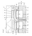
- the display D comprises an optical waveguide plate 12 for introducing light 10 thereinto, and a driving section 16 provided opposingly to the back surface of the optical waveguide plate 12 and including a large number of actuator elements 14 which are arranged corresponding to picture elements (image pixels).
- the display section 16 includes a substrate 18 composed of, for example, a ceramic.
- the actuator elements 14 are arranged at positions corresponding to the respective picture elements on the substrate 18.
- the substrate 18 has its first principal surface which is arranged to oppose to the back surface of the optical waveguide plate 12.
- the first principal surface is a continuous surface (flushed surface).
- Hollow spaces 20 for forming respective vibrating sections as described later on are provided at positions corresponding to the respective picture elements at the inside of the substrate 18.
- the respective hollow spaces 20 communicate with the outside via through-holes 18a each having a small diameter and provided at a second principal surface of the substrate 18.
- the portion of the substrate 18, at which the hollow space 20 is formed, is thin-walled.
- the other portion of the substrate 18 is thick-walled.
- the thin-walled portion has a structure which tends to undergo vibration in response to external stress, and it functions as a vibrating section 22.
- the portion other than the hollow space 20 is thick-walled, and it functions as a fixed section 24 for supporting the vibrating section 22.
- the substrate 18 has a stacked structure comprising a substrate layer 18A as a lowermost layer, a spacer layer 18B as an intermediate layer, and a thin plate layer 18C as an uppermost layer.
- the substrate 18 can be recognized as an integrated structure including the hollow spaces 20 formed at the positions in the spacer layer 18B corresponding to the picture elements.
- the substrate layer 18A functions as a substrate for reinforcement, as well as it functions as a substrate for wiring.
- the substrate 18 may be sintered in an integrated manner, or it may be additionally attached.
- each of the actuator elements 14 comprises the vibrating section 22 and the fixed section 24 described above, as well as a main actuator element 30 including a shape-retaining layer 26 composed of, for example, a piezoelectric/electrostrictive layer or an anti-ferroelectric layer directly formed on the vibrating section 22 and a pair of electrodes 28 (a row electrode 28a and a column electrode 28b) formed on an upper surface of the shape-retaining layer 26, and a displacement-transmitting section 32 connected onto the main actuator element 30 as shown in FIG. 1, for increasing the contact area with respect to the optical waveguide plate 12 to obtain an area corresponding to the picture element.
- a shape-retaining layer 26 composed of, for example, a piezoelectric/electrostrictive layer or an anti-ferroelectric layer directly formed on the vibrating section 22 and a pair of electrodes 28 (a row electrode 28a and a column electrode 28b) formed on an upper surface of the shape-retaining layer 26, and a displacement-transmitting section 32 connected onto the main actuator element 30 as shown in
- the display D has the structure in which the main actuator elements 30 comprising the shape-retaining layers 26 and the pairs of electrodes 28 are formed on the substrate 18.
- the pair of electrodes 28 may have a structure in which they are formed on upper and lower sides of the shape-retaining layer 26, or they are formed on only one side of the shape-retaining layer 26.
- the pair of electrodes 28 are formed only on the upper side (the side opposite to the substrate 18) of the shape-retaining layer 26 so that the substrate 18 directly contacts with the shape-retaining layer 26 without any difference in height, as in the display D.
- the hollow space 20, which is formed in the substrate 18, has a circular circumferential superficial configuration, i.e., the vibrating section 22 has a circular planar configuration (see broken lines).
- the shape-retaining layer 26 has a circular planar configuration (see chain lines).
- the pair of electrodes 28 form an outer circumferential configuration which is circular as well (see solid lines).
- the vibrating section 22 is designed to have the largest size.
- the outer circumferential configuration of the pair of electrodes 28 is designed to have the second largest size.
- the planar configuration of the shape-retaining layer 26 is designed to have the smallest size. Alternatively, it is allowable to make design so that the outer circumferential configuration of the pair of electrodes 28 is largest.
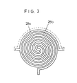
- the pair of electrodes 28 (row electrodes 28a and column electrodes 28b) formed on the shape-retaining layer 26 have, for example, a spiral planar configuration as shown in FIG. 3, in which the pair of electrodes 28a, 28b are parallel to one another and separated from each other to form a spiral structure composed of several turns.
- the number of turns of the spiral is actually not less than 5 turns.
- FIG. 3 illustratively shows 3 turns in order to avoid complicated illustration.
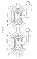
- the wiring arrangement communicating with the respective electrodes 28a, 28b includes vertical selection lines 40 having a number corresponding to a number of rows of a large number of the picture elements, and signal lines 42 having a number corresponding to a number of columns of the large number of the picture elements.
- Each of the vertical selection lines 40 is electrically connected to the row electrode 28a of each of the picture elements (actuator elements 14, see FIG. 1).
- Each of the signal lines 42 is electrically connected to the column electrode 28b of each of the picture elements 14.
- the respective vertical selection lines 40 which are included in one row, are wired in series such that the wiring is led from the row electrode 28a provided for the picture element in the previous column, and then the wiring is connected to the row electrode 28a provided for the picture element in the present column.
- the signal line 42 comprises a main line 42a extending in the direction of the column, and branch lines 42b branched from the main line 42a and connected to the column electrode 28b of each of the picture elements 14.
- the voltage signal is supplied to the respective vertical selection lines 40 from an unillustrated wiring board (stuck to the second principal surface of the substrate 18) via through-holes 44.
- the voltage signal is also supplied to the respective signal lines 42 from the unillustrated wiring board via through-holes 46.
- the through-holes 44 for the vertical selection lines 40 are formed as follows provided that the number of rows is M, and the number of columns is N.
- the through-hole 44 for the vertical selection line 40 is not formed on the vertical selection line 40, unlike the through-hole 46 for the signal line 42. Accordingly, a relay conductor 48 is formed between the through-hole 44 and the row electrode 28a, for making electric continuity therebetween.
- Insulative films 50 are allowed to intervene at portions of intersection between the respective vertical selection lines 40 and the respective signal lines 42, in order to ensure insulation between the mutual wiring arrangements 40, 42.
- the planar configuration of the pair of electrodes 28 is not limited to the spiral configuration as shown in FIG. 3.
- the planar configuration may be a configuration as shown in FIG. 4.
- each of the pair of electrodes 28a, 28b has a configuration composed of a trunk 52, 54 which extends toward the center of the shape-retaining layer 26, and a lot of branches 56, 58 branched from the trunk 52, 54.
- the pair of electrodes 28a, 28b are separated from each other and arranged complementarily (hereinafter referred to as "branched configuration" for convenience).
- the display D constructed as described above has been explained as one having the circular planar configuration of the vibrating section 22, the circular planar configuration of the shape-retaining layer 26, and the circular outer circumferential configuration formed by the pair of electrodes 28.
- both of the planar configuration of the vibrating section 22 and the planar configuration of the shape-retaining layer 26 may be rectangular configurations with smoothed corners as shown in FIG. 8. Further alternatively, both of the planar configuration of the vibrating section 22 and the planar configuration of the shape-retaining layer 26 may be polygonal configurations (for example, octagonal configurations) with respective apex angle portions having rounded shapes as shown in FIG. 9.
- the configuration of the vibrating section 22, the planar configuration of the shape-retaining layer 26, and the outer circumferential configuration formed by the pair of electrodes 28 may be combinations of circular and elliptic configurations, or combinations of rectangular and elliptic configurations, without any special limitation.
- those preferably adopted as the planar configuration of the shape-retaining layer 26 include a ring-shaped configuration.
- those usable as the outer circumferential configuration include various ones such as circular, elliptic, and rectangular configurations.
- the ring-shaped planar configuration of the shape-retaining layer 26 makes it unnecessary to form any electrode on the hollow portion. Therefore, it is possible to decrease the electrostatic capacity without decreasing the displacement amount.
- the respective actuator elements 14 are illustratively arranged in the matrix form on the substrate 18.
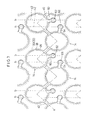
- the picture elements (actuator elements) 14 may be arranged in a zigzag form with respect to the respective rows.
- the actuator elements (picture elements) 14 are arranged in the zigzag form in relation to the respective rows. Accordingly, the line (indicated by a chain line "a") connecting through the vertical selection lines 40 respectively has a zigzag form in relation to each of the rows.
- the signal lines 42 have a wiring pattern as shown by broken lines "b" wired on the unillustrated wiring board, in which the picture elements 14 arranged in the zigzag form are divided, for example, into a group of picture elements (actuator elements) 14 located vertically upwardly and a group of picture elements (actuator elements) 14 located vertically downwardly, and two signal lines 42 are wired mutually adjacently at positions corresponding to the former and latter groups of picture elements.
- the picture elements arranged in the zigzag form are wired as follows.
- the column electrode 28b of the picture element (actuator element) 14 located vertically upwardly is electrically connected to the right signal line 42 of the mutually adjacent two signal lines 42, 42, via a relay conductor 60 and a through-hole 62.
- the column electrode 28b of the picture element (actuator element) 14 located vertically downwardly is electrically connected to the left signal line 42 of the mutually adjacent two signal lines 42, 42, via a relay conductor 64 and a through-hole 66.
- those usable as the piezoelectric/electrostrictive layer include ceramics containing, for example, lead zirconate, lead magnesium niobate, lead nickel niobate, lead zinc niobate, lead manganese niobate, lead magnesium tantalate, lead nickel tantalate, lead antimony stannate, lead titanate, barium titanate, lead magnesium tungstate, and lead cobalt niobate, as well as any combination of them.
- the major component contains the compound as described above in an amount of not less than 50 % by weight.
- the ceramic containing lead zirconate is most frequently used as the constitutive material of the piezoelectric/electrostrictive layer according to the embodiment of the present invention.
- the piezoelectric/electrostrictive layer is composed of a ceramic
- ceramics obtained by appropriately adding, to the ceramics described above, oxide of, for example, lanthanum, calcium, strontium, molybdenum, tungsten, barium, niobium, zinc, nickel, and manganese, or any combination thereof or another type of compound thereof.
- oxide of, for example, lanthanum, calcium, strontium, molybdenum, tungsten, barium, niobium, zinc, nickel, and manganese or any combination thereof or another type of compound thereof.
- a ceramic containing a major component composed of lead magnesium niobate, lead zirconate, and lead titanate and further containing lanthanum and strontium.
- the piezoelectric/electrostrictive layer may be either dense or porous. When the piezoelectric/electrostrictive layer is porous, its porosity is preferably not more than 40 %.
- the anti-ferroelectric layer is used as the shape-retaining layer 26, it is desirable to use, as the anti-ferroelectric layer, a compound containing a major component composed of lead zirconate, a compound containing a major component composed of lead zirconate and lead stannate, a compound obtained by adding lanthanum to lead zirconate, and a compound obtained by adding lead zirconate and lead niobate to a component composed of lead zirconate and lead stannate.
- an anti-ferroelectric film which contains a component comprising lead zirconate and lead stannate as represented by the following composition, is applied as a film-type element such as the anti-ferroelectric film-type element, it is possible to perform driving at a relatively low voltage. Therefore, application of such an anti-ferroelectric film is especially preferred.
- the anti-ferroelectric layer may be porous.
- the anti-ferroelectric layer is porous, it is desirable that the porosity is not more than 30 %.
- the light 10 is introduced, for example, from the end portion of the optical waveguide plate 12.
- all of the light 10 is totally reflected at the inside of the optical waveguide plate 12 without being transmitted through the front and back surfaces thereof by controlling the magnitude of the refractive index of the optical waveguide plate 12.
- a part of the scattered light 70 is reflected again in the optical waveguide plate 12.
- almost all of the scattered light 70 is not reflected by the optical waveguide plate 12, and it is transmitted through the front surface of the optical waveguide plate 12.
- the presence or absence of light emission (leakage light) at the front surface of the optical waveguide plate 12 can be controlled depending on the presence or absence of the contact of the displacement-transmitting section 32 disposed at the back of the optical waveguide plate 12.
- one unit for making the displacement action of the displacement-transmitting section 32 in the direction to make contact or separation with respect to the optical waveguide plate 12 may be recognized as one picture element.
- a large number of the picture elements are arranged in a matrix configuration or in a zigzag configuration concerning the respective rows.
- the bending displacement characteristic shown in FIG. 10 is obtained by applying a voltage between the pair of electrodes 28a, 28b of the main actuator element 30 to perform a polarization treatment for the shape-retaining layer 26, and then observing the bending displacement of the actuator element 14 while continuously changing the voltage applied to the actuator element 14.
- the direction of bending displacement is positive when the actuator element 14 makes bending displacement in a first direction (direction to make approach to the optical waveguide plate 12).
- the measurement of the bending displacement characteristic will be specifically explained with reference to an example.
- a voltage is applied between the pair of electrodes 28a, 28b to perform the polarization treatment for the shape-retaining layer 26 to perform the polarization treatment for the shape-retaining layer 26.
- an electric field in the positive direction is generated in the superficial direction around the first principal surface of the shape-retaining layer 26.
- the intensity of the electric field generated in the shape-retaining layer 26 is largest at the first principal surface, and it is gradually decreased in the depth direction. Therefore, it is difficult to advance the polarization at deep portions.
- the polarization can be allowed to proceed to portions located in the depth direction by applying a sufficient electric field and an appropriate amount of heat for a sufficient period of time.
- the polarization treatment is achieved in the same direction as that of the generated electric field.
- FIG. 10 shows a bending displacement characteristic obtained by plotting results of the measurement on a graph of electric field-bending displacement. As indicated by arrows in FIG. 10, the displacement amount of the bending displacement continuously changes in accordance with continuous increase and decrease in applied voltage while providing a certain degree of hysteresis.
- the direction of polarization in the shape-retaining layer 26 is coincident with the direction of the electric field brought about by the applied voltage, and the electric field is applied intensely in the vicinity of the surface of the shape-retaining layer 26. Therefore, the shape-retaining layer 26 is elongated in the horizontal direction, and the actuator element 14 makes bending displacement in the first direction (the direction to make approach to the optical waveguide plate 12).
- the convex displacement of the actuator element 14 allows the displacement-transmitting section 32 to make displacement toward the optical waveguide plate 12, and the displacement-transmitting section 32 contacts with the optical waveguide plate 12.
- the displacement-transmitting section 32 contacts with the back surface of the optical waveguide plate 12 in response to the bending displacement of the main actuator element 30.
- the displacement-transmitting section 32 contacts with the back surface of the optical waveguide plate 12, for example, the light 10, which has been totally reflected in the optical waveguide plate 12, is transmitted through the back surface of the optical waveguide plate 12, and it is transmitted to the surface of the displacement-transmitting section 32.
- the light 10 is reflected by the surface of the displacement-transmitting section 32. Accordingly, the picture element corresponding to the actuator element 14 is in the ON state.
- the displacement-transmitting section 32 is provided to reflect the light transmitted through the back surface of the optical waveguide plate 12, and it is provided to increase the contact area with respect to the optical waveguide plate 12 to be not less than a predetermined size. That is, the light emission area is determined by the contact area between the displacement-transmitting section 32 and the optical waveguide plate 12.
- the displacement-transmitting section 32 includes the plate member 32a for determining the substantial light emission area, and the displacement-transmitting member 32b for transmitting the displacement of the main actuator element 30 to the plate member 32a.
- the contact between the displacement-transmitting section 32 and the optical waveguide plate 12 means the fact that the displacement-transmitting section 32 and the optical waveguide plate 12 are positioned at a distance of not more than the wavelength of the light 10 (light 10 introduced into the optical waveguide plate 12).
- portions other than the plate member 32a which makes contact with the optical waveguide plate 12 are covered with a black matrix.
- a metal film such as those made of Cr, Al, Ni, and Ag as the black matrix, because of the following reason. That is, such a metal film absorbs a small amount of light, and hence it is possible to suppress attenuation and scattering of the light transmitted through the optical waveguide plate 12. Therefore, such a metal film is used especially preferably.
- the actuator element 14 intends to make restoration from the convex state to the original state (state indicated by Point B).
- the actuator element 14 does not undergo complete restoration to the state of Point B, and it gives a state in which it is slightly displaced in the first direction from Point B (state indicated by Point H).
- the displacement-transmitting section 32 and the optical waveguide plate 12 are in a state in which they are separated from each other, i.e., in the OFF state.
- the ON state is maintained owing to the memory function (hysteresis characteristic) of the shape-retaining layer 26 even when the applied voltage is lowered, for example, up to 30 V to 80 V after giving the ON state by applying the positive peak voltage between the pair of electrodes 28a, 28b.
- the memory function is also effected in the OFF state in the same manner as described above.
- the OFF state is maintained owing to the memory function (hysteresis characteristic) of the shape-retaining layer 26 even when the applied voltage is raised, for example, up to 30 V to 80 V after giving the OFF state by applying 0 V or the negative peak voltage between the pair of electrodes 28a, 28b.
- the actuator element 14 having the shape-retaining layer 26 can be defined as an actuator element which has at least two or more displacement states at an identical voltage level.
- the actuator element 14 having the shape-retaining layer 26 has the following features.
- an actuator element 14 which makes, for example, upward displacement (giving the separated state upon no voltage load and giving the contact state upon voltage application) because of easiness of control.
- the structure having the pair of electrodes 28a, 28b on the surface is desirable.
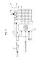
- the driving device 100 comprises a row electrode-driving circuit for selectively supplying a driving signal to the vertical selection lines 40 (connected in series to the row electrodes 28a of the actuator elements 14 for the respective rows) for the display section 16 comprising a large number of actuator elements 14 arranged in the matrix configuration or in the zigzag configuration so that the actuator elements 14 are successively selected in one row unit, a column electrode-driving circuit 104 for outputting a data signal in parallel to the signal lines 42 for the display section 16 so that the data signal is supplied to the column electrodes 28b of the respective actuator elements 14 on the line (selected line) selected by the row electrode-driving circuit 102 respectively, and a signal control circuit 106 for controlling the row electrode-driving circuit 102 and the column electrode-driving circuit 104 on the basis of a picture image signal Sv and a synchronization signal Ss to be inputted.
- a row electrode-driving circuit for selectively supplying a driving signal to the vertical selection lines 40 (connected in series to the
- a logic power source voltage for example, ⁇ 5 V
- three types of row side power source voltages for example, 20 V, -30 V, and -80 V
- the logic power source voltage and two types of column side power source voltages are supplied to the column electrode-driving circuit 104 by the aid of the unillustrated power source circuit.
- the signal control circuit 106 comprises, at its inside, a timing controller, a frame memory, and an I/O buffer, which is constructed such that the row electrode-driving circuit 102 and the column electrode-driving circuit 104 are subjected to gradation control on the basis of the temporal modulation system via a row side control line 108 communicating with the row electrode-driving circuit 102 and a column side control line 110 communicating with the column electrode-driving circuit 104.
- the row electrode-driving circuit 102 and the column electrode-driving circuit 104 have the following features.
- the display period for one image is assumed to be one field.
- Those set for the one field include a period (hereinafter referred to as "light source turn on period”) Tb for radiating the light from the light source to the optical waveguide plate 12 shown in FIG. 1, and a period (hereinafter referred to as “light source turn off period”) Tc for stopping the radiation of the light from the light source to the optical waveguide plate 12.
- An overall bending displacement period Td for making bending displacement of all of the actuator elements 14 is set within the light source turn off period Tc.
- a gradational display period Te for performing substantial gradational display, and a reset period T R for resetting the bending displacement of all of the actuator elements 14 are set within the light source turn on period Tb.
- the time, which extends from the point of time of application of a voltage (for example, +130 V) sufficient to make the bending displacement to the actuator element 14 for constructing the picture element until light emission of the picture element as a result of the bending displacement of the actuator element 14, is defined as "light-emitting rising time Tr of the picture element”.
- the time, which extends from the point of time of application of a voltage (for example, -20 V) sufficient to reset the bending displacement to the actuator element 14 until quenching of the picture element as a result of the reset of the bending displacement of the actuator element 14, is defined as "quenching falling time Tf of the picture element".
- the overall bending displacement period Td is set, which extends from the start point of time t0 of one field to at least the light-emitting rising time Tr of the picture element or which extends thereover.
- the light source turn on period Tb i.e., the gradational display period Te
- the light source turn on period Tb is started from a point of time t2 after passage of one subfield SF0 from an end point of time t1 of the overall bending displacement period Td.
- a number of subfields (SF1 to SFn) corresponding to the maximum gradation level are set in the gradational display period Te.
- the row electrode-driving circuit 102 is subjected to timing control by the signal control circuit 106 so that all row selection is completed in each of the subfields SF1 to SFn.
- the time for the row electrode-driving circuit 102 to select one row is regulated by the time width obtained by dividing one subfield by the number of rows of the driving section 16.
- the time width described above or a time shorter than the time width is selected.
- 1/n of the time width (n is an arbitrary real number from 1 to 5, preferably a real number from 1 to 3) is selected.
- the time for selecting one row by using the row electrode-driving circuit 102 corresponds to the time for switching the address for the driving section 16. Therefore, the foregoing time may be defined as "address time Ta".
- each of the subfields is divided into a selection period Ts and an unselection period Tu.
- the selection period Ts is set to be the same period of time as the address time Ta described above.
- the reset period T R is a period corresponding to one subfield.
- the signal control circuit 106 is used to prepare a data signal for each picture element concerning the selected row by allotting the display time corresponding to each gradation level to each of the subfields SF1 to SFn.
- the data signal is outputted during the selection period Ts of each of the subfields SF1 to SFn by the aid of the column electrode-driving circuit 104.
- the group of picture elements in the first row are selected by the row electrode-driving circuit 102.
- the data signal is supplied to the group of picture elements in the first row by the aid of the column electrode-driving circuit 104.
- the data signal, which is supplied to each of the picture elements is the data signal (for example, the ON signal and the OFF signal) prepared by allotting the display time corresponding to the gradation level to each of the subfields SF0 to SFn.
- the display time corresponding to the gradation level of the picture element is assigned to the time width allotted to each of the subfields SF0 to SFn. This procedure includes a case in which the assignment is made for all of the subfields SF0 to SFn, and a case in which the assignment is made for some of the subfields.
- the number of subfields is 10 (in this case, there are subfields SF0 to SF9).
- the picture element has 10 gradation levels, for example, all of the subfields SF0 to SF9 are selected.
- the gradation level is 6, the continuous subfields SF0 to SF5 are selected.
- the gradation level is 3, the continuous subfields SF0 to SF2 are selected.
- the output form of the data signal supplied to the picture element is as follows. That is, for example, it is possible to adopt a form in which the ON signal is outputted for the selected subfield, and the OFF signal is outputted for the unselected subfield.
- FIGs. 14 to 20 Two specified embodiments will now be explained with reference to FIGs. 14 to 20.
- the explanation is directed to only a display pattern (representing four gradation levels) for the picture element in the first column provided that the number of rows is 4 as shown in FIG. 14.
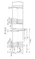
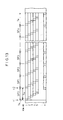
- Timing charts shown in FIGs. 16A to 16D, FIGs. 18A to 18D, FIGs. 19A to 19C, and FIGs. 20A to 20C illustrate respective waveforms of the column signal Sc for the first column, the row signal Sr for the first row, and the applied voltage Vp to the picture element in the first row first column.
- the row electrode-driving circuit 102 outputs a bending displacement pulse signal Pa which starts from the start point of time t0 of one field and which extends over the overall bending displacement period Td within the light source turn off period Tc.
- the row electrode-driving circuit 102 outputs a selection pulse signal Ps during the selection period Ts (address period Ta) in each of the subfields SF0 to SF4 after passage of the overall bending displacement period Td.
- the row electrode-driving circuit 102 outputs an unselection signal Su during the unselection period Tu in each of the subfields SF0 to SF4.
- the bending displacement pulse signal Pa has a pulse waveform in which the pulse width is approximately the same as the overall bending displacement period Td and the peak voltage is -80 V.
- the selection pulse signal Ps has a pulse waveform in which the pulse width is approximately the same as the selection period Ts (address time Ta) and the peak voltage is +20 V.
- the unselection signal Su is fixed at a reference level (-30 V) (see FIG. 15).
- the column electrode-driving circuit 104 outputs the ON signal with a peak voltage of +50 V having the same polarity as that of the selection pulse signal Ps, during the selection period Ts in the subfield allotted as the light emission objective, of the respective subfields SF0 to SF4.
- the column electrode-driving circuit 104 outputs the OFF signal at 0 V during the selection period Ts in the subfield as the quenching objective.
- the column electrode-driving circuit 104 outputs a signal at the same level as that of the ON signal during the overall bending displacement period Td. Therefore, during the overall bending displacement period Td as shown in FIG. 16C, the ON signal (+50 V) is applied to the column electrode 28b, and the bending displacement pulse signal (-80 V) is applied to the row electrode 28a. Accordingly, the applied voltage Vp between the pair of electrodes 28a, 28b of the picture element is 130 V. Thus, all of the picture elements are in the ON state according to the bending displacement characteristic shown in FIG. 10. However, no light is introduced from the light source into the optical waveguide plate 12. Therefore, all of the picture elements do not cause any light emission, and all of them are in the quenching state.
- the temporal length of each of the subfields SF0 to SF4 is, for example, a length corresponding to four address times (4 ⁇ Ta). Therefore, when observation is made for the picture element in the first row, the selection period Ts is the initial first address time of one subfield (for example, the subfield SF1), and the unselection period Tu is the remaining and continuous second to fourth address times.
- the selection period Ts is deviated by every one address time Ta.
- the selection periods Ts for the respective picture elements in the second, third, and fourth row appear at timings corresponding to the second, third, and fourth address times respectively, when the row signal Sr for the first picture element is used as a standard.
- the OFF signal is outputted at the timing of the first and second address times in the subfield SF2, and the ON signal is outputted during the other period, because it is necessary to turn off the picture elements in the first and second rows.
- the ON signal when observation is directed to the picture element in the first row, if the ON signal is outputted during the selection period Ts as in the subfields SF0 and SF1, then the ON signal (+50 V) is applied to the column electrode 28b during the selection period Ts, and the selection pulse signal Ps (+20 V) is applied to the row electrode 28a. Accordingly, the applied voltage Vp between the pair of electrodes 28a, 28b of the picture element is +30 V.
- the actuator element 14 for the concerning picture element undergoes the displacement at +30 V (see Point C), and the bending displacement of the actuator element 14 is maintained as it is.
- the concerning picture element is in the ON state.
- the subfield SF0 is included in the light source turn off period Tc, and hence the quenching state is still maintained even when the picture element is in the ON state.
- the light source turn on period Tb starts from the start point of time t2 of the subfield SF1, and the light is introduced from the light source into the optical waveguide plate 12. Therefore, the concerning picture element causes light emission.
- the OFF signal when the OFF signal is outputted during the selection period Ts as in the subfield SF2, the OFF signal (0 V) is applied to the column electrode 28b during the selection period Ts, and the selection pulse signal Ps (+20 V) is applied to the row electrode 28a. Therefore, the applied voltage Vp between the pair of electrodes 28a, 28b of the concerning picture element is -20 V.
- the bending displacement of the actuator element 14 corresponding to the concerning picture element is reset, and the concerning picture element is in the OFF state and quenched.
- the OFF signal is continuously outputted at timings of the first to third address times in the subfield SF3, and the ON signal is outputted during the other period, i.e., during the fourth address time.
- the picture element in the third row is also in the OFF state and quenched.
- the OFF signal is continuously outputted during the entire period of the subfield SF4.
- the picture element in the fourth row is also in the OFF state and quenched. That is, all of the picture elements are quenched.
- the image is displayed on the screen of the display by successively repeating the series of operations described above.
- the first embodiment as described above, it is unnecessary to perform, for example, complicated voltage switch and voltage selection even when the range of display gradation of each of the picture elements is widened. Therefore, it is possible to suppress the setting number of working voltages to the minimum.
- the actuator element 14 for constructing each of the picture elements has the memory function for the bending displacement.
- the peak value of the pulse signal for the row selection is a voltage value at which the actuator element 14 sufficiently makes the bending displacement in the first direction
- the voltage value during the unselection period Tu thereafter is set within a range in which the actuator element 14 is capable of storing the displacement. Therefore, it is possible to easily control the actuator element 14 in accordance with the temporal modulation system.
- the voltage value during the unselection period Tu is set to be the voltage value described above (voltage value within the range in which the actuator element 14 is capable of storing the displacement). Therefore, the selection period Ts can be made further short, for example, it can be made short up to the address time Ta.
- the light-emitting rising time Tr of the picture element is sometimes extremely longer than the quenching falling time Tf of the picture element.
- Such a procedure causes a problem that the time of the gradational display period Te to make contribution to light emission is shortened, and it is disadvantageous to extend the gradation level.
- the actuator elements 14 are subjected to the bending displacement during the light source turn off period Tc before the start of the gradational display period Te. Therefore, the light emission is performed for the period of time corresponding to the gradation level of each of the picture elements in the next gradational display period Te. After that, the bending displacement of the actuator element 14 corresponding to the picture element is reset to successfully turn off the picture element. Accordingly, it is unnecessary to set any preparatory period (delay time) for making the bending displacement of the actuator element 14 during the gradational display period Te. This results in maximum utilization of the limited gradational display period Te, making it possible to obtain an effect of advantage to extend the gradation level of the picture element.
- the data signal for another row (ON signal and OFF signal) successively appears during the unselection period Tu for each of the subfields. That is, as for one picture element, the voltage waveform of the concerning picture element during the unselection period Tu is determined depending on the pattern of the data signal (appearance pattern of the ON signal and the OFF signal) for the rows other than the row to which the concerning picture element belongs in the column to which the concerning picture element belongs.
- the average voltage of the concerning picture element during the unselection period Tu is fixed at a voltage level (conveniently referred to as "high voltage level (80 V)") obtained by subtracting the reference level (-30 V) from the voltage level (50 V) of the ON signal as shown by a chain line "c" in FIG. 16C.
- the average voltage is fixed at a voltage level (conveniently referred to as "low voltage level (30 V)" obtained by subtracting the reference level (-30 V) from the voltage level (0 V) of the OFF signal as shown by a broken line “d” in FIG. 16C.
- the average voltage is an intermediate voltage between the high voltage level (80 V) and the low voltage level (30 V).
- the bending displacement of the actuator element 14 during the unselection period Tu is delicately changed depending on the voltage change (voltage change depending on the pattern of the ON signal and the OFF signal).
- the ON signal or the OFF signal is outputted for a cluster of a large number of rows, the difference in average voltage is large. Therefore, there is a possibility that the display state (brightness and gradation) of the concerning picture element during the unselection period Tu may become unstable.
- the second embodiment described below resides in a system to solve the problem described above, in which phase information is added to the ON signal, the OFF signal, and the selection pulse signal Ps.
- the second embodiment is also directed to only the display pattern of the picture elements in the first column with the number of four rows (representing the four gradation levels), in the same manner as the first embodiment described above. It is assumed that the gradation level of the picture element in the first row is 2, the gradation level of the picture element in the second row is 1, the gradation level of the picture element in the third row is 3, and the gradation level of the picture element in the fourth row is 4 (see FIG. 14).
- the second embodiment resides in the system in which the phase information is added to the ON signal, the OFF signal, and the selection pulse signal Ps respectively.
- the ON signal has a waveform in which it rises simultaneously with the start of the selection period Ts, and it has a pulse width which is 1/2 of the address time Ta.
- the OFF signal has a phase opposite to that of the ON signal.
- the selection pulse signal Ps has the same phase as that of the ON signal.
- the output timing of the unselection signal Su is the same as that of the first embodiment.
- each of the ON signal, the OFF signal, and the selection pulse signal Ps constitutes a pulse signal in which the high level and the low level exist in a mixed manner within one address time Ta.
- the signal-processing operation performed in the second embodiment is the same as that performed in the first embodiment. Therefore, detailed explanation thereof will be omitted.
- both of the average voltages during the unselection period Tu are 55 V for the case in which the ON signal is outputted for all of the other rows and the case in which the OFF signal is outputted for all of the other rows.
- the difference between these average voltages is 0 V.
- the pulse signal continuously appears during the unselection period Tu. Therefore, the average voltage during the unselection period Tu does not depend on the pattern of the ON signal and the OFF signal, and it has an approximately constant value. Thus, the display state (brightness and gradation) is stabilized during the unselection period Tu.
- the waveform of the selection pulse signal Ps is the waveform having the same phase as that of the ON signal.
- the second embodiment makes it possible to obtain an effect that the limited gradational display period can be maximally utilized to give an advantage to extend the gradation level of the picture element even when the light-emitting rising time Tr of the picture element is extremely longer than the quenching falling time Tf of the picture element.
- the OFF signal is outputted over the reset period T R , in the same manner as the subfield SF4. The bending displacement of the actuator element 14 can be reliably reset by providing the reset period T R as described above, making it possible to easily respond to the display of animation images in the same manner as the first and second embodiments.
- the scanning is performed one after another from the first row to the fourth row when the picture element array concerning one row is subjected to the scanning.
- the scanning may be performed one after another from the first row to the final row in one field (for example, odd number field), and the scanning may be performed one after another from the final row to the first row in the next field (for example, even number field). It is possible to avoid the occurrence of discrepancy corresponding to one gradation between the picture element in the first row and the picture element in the final row, making it possible to improve the image quality.
- the display D to which the driving device 100 according to the embodiment is applied, includes the pair of electrodes 28a, 28b which are formed in such a form that the row electrode 28a and the column electrode 28b are formed on the surface of the shape-retaining layer 26.
- the row electrode 28a is formed on the lower surface of the shape-retaining layer 26, and the column electrode 28b is formed on the upper surface of the shape-retaining layer 26.
- the display-driving device and the display-driving method according to the present invention are not limited to the embodiments described above. It is a matter of course that various constructions may be adopted therefor without deviating from the gist or essential characteristics of the present invention.
Landscapes
- Engineering & Computer Science (AREA)
- Physics & Mathematics (AREA)
- Computer Hardware Design (AREA)
- General Physics & Mathematics (AREA)
- Theoretical Computer Science (AREA)
- Control Of Indicators Other Than Cathode Ray Tubes (AREA)
- Devices For Indicating Variable Information By Combining Individual Elements (AREA)
- Mechanical Light Control Or Optical Switches (AREA)
Applications Claiming Priority (3)
| Application Number | Priority Date | Filing Date | Title |
|---|---|---|---|
| JP19451997A JP3437743B2 (ja) | 1997-07-18 | 1997-07-18 | ディスプレイの駆動装置及びディスプレイの駆動方法 |
| JP19451997 | 1997-07-18 | ||
| JP194519/97 | 1997-07-18 |
Publications (2)
| Publication Number | Publication Date |
|---|---|
| EP0903720A2 true EP0903720A2 (fr) | 1999-03-24 |
| EP0903720A3 EP0903720A3 (fr) | 1999-07-21 |
Family
ID=16325892
Family Applications (1)
| Application Number | Title | Priority Date | Filing Date |
|---|---|---|---|
| EP98305666A Withdrawn EP0903720A3 (fr) | 1997-07-18 | 1998-07-16 | Commande de gradation pour un dispositif d'affichage comportant un guide plan d'ondes optiques |
Country Status (3)
| Country | Link |
|---|---|
| US (1) | US6452583B1 (fr) |
| EP (1) | EP0903720A3 (fr) |
| JP (1) | JP3437743B2 (fr) |
Cited By (3)
| Publication number | Priority date | Publication date | Assignee | Title |
|---|---|---|---|---|
| WO2001067428A1 (fr) * | 2000-03-10 | 2001-09-13 | Ngk Insulators, Ltd. | Procede de production d'un dispositif d'affichage |
| WO2003079317A3 (fr) * | 2002-03-20 | 2004-12-29 | Koninkl Philips Electronics Nv | Procede de commande d'un ecran d'affichage a feuille et dispositif comprenant un tel ecran d'affichage |
| WO2007120949A3 (fr) * | 2006-01-24 | 2008-01-17 | Uni Pixel Displays Inc | Microstructures optiques pour l'extraction et la commande de lumière |
Families Citing this family (22)
| Publication number | Priority date | Publication date | Assignee | Title |
|---|---|---|---|---|
| EP0907212A1 (fr) * | 1996-11-29 | 1999-04-07 | Ngk Insulators, Ltd. | Element ceramique, procede de fabrication d'un element ceramique, ceramique, dispositif de relais, et condensateur |
| JP4637315B2 (ja) * | 1999-02-24 | 2011-02-23 | 株式会社半導体エネルギー研究所 | 表示装置 |
| US7193594B1 (en) * | 1999-03-18 | 2007-03-20 | Semiconductor Energy Laboratory Co., Ltd. | Display device |
| US7145536B1 (en) * | 1999-03-26 | 2006-12-05 | Semiconductor Energy Laboratory Co., Ltd. | Liquid crystal display device |
| US7472910B1 (en) * | 1999-03-30 | 2009-01-06 | Canon Kabushiki Kaisha | Animation display apparatus, arcade game machine, control method and apparatus thereof, and storage medium |
| US6952194B1 (en) * | 1999-03-31 | 2005-10-04 | Semiconductor Energy Laboratory Co., Ltd. | Liquid crystal display device |
| US6753854B1 (en) | 1999-04-28 | 2004-06-22 | Semiconductor Energy Laboratory Co., Ltd. | Display device |
| US7081928B2 (en) * | 2001-05-16 | 2006-07-25 | Hewlett-Packard Development Company, L.P. | Optical system for full color, video projector using single light valve with plural sub-pixel reflectors |
| CN1596430A (zh) * | 2001-11-26 | 2005-03-16 | 皇家飞利浦电子股份有限公司 | 包含光波导板的显示设备及其操作方法 |
| JP2005521096A (ja) * | 2002-03-26 | 2005-07-14 | コーニンクレッカ フィリップス エレクトロニクス エヌ ヴィ | 光伝送プレート及び光吸収手段を有するディスプレイ装置 |
| US6879307B1 (en) * | 2002-05-15 | 2005-04-12 | Ernest Stern | Method and apparatus for reducing driver count and power consumption in micromechanical flat panel displays |
| US20030227447A1 (en) * | 2002-06-04 | 2003-12-11 | Ngk Insulators, Ltd. | Display device |
| US20030227449A1 (en) * | 2002-06-05 | 2003-12-11 | Ngk Insulators, Ltd. | Display device |
| US7006061B2 (en) * | 2002-06-04 | 2006-02-28 | Ngk Insulators, Ltd. | Display device |
| US7141915B2 (en) * | 2003-07-22 | 2006-11-28 | Ngk Insulators, Ltd. | Actuator device |
| WO2005008798A1 (fr) * | 2003-07-22 | 2005-01-27 | Ngk Insulators, Ltd. | Actionneur |
| US20070064008A1 (en) * | 2005-09-14 | 2007-03-22 | Childers Winthrop D | Image display system and method |
| US20070064007A1 (en) * | 2005-09-14 | 2007-03-22 | Childers Winthrop D | Image display system and method |
| US20070063996A1 (en) * | 2005-09-14 | 2007-03-22 | Childers Winthrop D | Image display system and method |
| US7551154B2 (en) * | 2005-09-15 | 2009-06-23 | Hewlett-Packard Development Company, L.P. | Image display system and method |
| JP5367383B2 (ja) * | 2009-01-14 | 2013-12-11 | 株式会社東芝 | 表示装置及びその駆動方法 |
| JP5834418B2 (ja) * | 2011-02-04 | 2015-12-24 | セイコーエプソン株式会社 | 光フィルター、光フィルターモジュール、分析機器及び光機器 |
Family Cites Families (25)
| Publication number | Priority date | Publication date | Assignee | Title |
|---|---|---|---|---|
| US2565514A (en) * | 1947-12-01 | 1951-08-28 | Int Standard Electric Corp | Radiation intensity modulator |
| US2997922A (en) * | 1958-04-24 | 1961-08-29 | Edward K Kaprelian | Light valve |
| US3376092A (en) * | 1964-02-13 | 1968-04-02 | Kollsman Instr Corp | Solid state display composed of an array of discrete elements having movable surfaces |
| US3698793A (en) | 1971-03-11 | 1972-10-17 | Kollsman Instr Corp | Solid state display |
| US3812490A (en) | 1972-09-18 | 1974-05-21 | Bendix Corp | Flexible membrane display panel for generating characters visible in ambient light |
| US4113360A (en) | 1977-03-28 | 1978-09-12 | Siemens Aktiengesellschaft | Indicating device for illustrating symbols of all kinds |
| US4234245A (en) * | 1977-04-22 | 1980-11-18 | Rca Corporation | Light control device using a bimorph element |
| JPH01185692A (ja) * | 1988-01-19 | 1989-07-25 | Sanyo Electric Co Ltd | 平面ディスプレイパネル |
| US5106181A (en) * | 1989-04-12 | 1992-04-21 | Rockwell Iii Marshall A | Optical waveguide display system |
| JP2886588B2 (ja) | 1989-07-11 | 1999-04-26 | 日本碍子株式会社 | 圧電/電歪アクチュエータ |
| US5319491A (en) * | 1990-08-10 | 1994-06-07 | Continental Typographics, Inc. | Optical display |
| US5521746A (en) * | 1993-02-22 | 1996-05-28 | Engle; Craig D. | Poppet valve modulator |
| US5452024A (en) * | 1993-11-01 | 1995-09-19 | Texas Instruments Incorporated | DMD display system |
| US6049158A (en) | 1994-02-14 | 2000-04-11 | Ngk Insulators, Ltd. | Piezoelectric/electrostrictive film element having convex diaphragm portions and method of producing the same |
| JP3187669B2 (ja) * | 1994-04-01 | 2001-07-11 | 日本碍子株式会社 | ディスプレイ素子及びディスプレイ装置 |
| JP3139312B2 (ja) | 1994-11-25 | 2001-02-26 | 株式会社富士通ゼネラル | ディスプレイ駆動方法および装置 |
| US5668611A (en) * | 1994-12-21 | 1997-09-16 | Hughes Electronics | Full color sequential image projection system incorporating pulse rate modulated illumination |
| US5563977A (en) * | 1995-05-24 | 1996-10-08 | General Electric Company | Display system having greyscale control of fiber optic delivered light output |
| US5771321A (en) * | 1996-01-04 | 1998-06-23 | Massachusetts Institute Of Technology | Micromechanical optical switch and flat panel display |
| US5731802A (en) * | 1996-04-22 | 1998-03-24 | Silicon Light Machines | Time-interleaved bit-plane, pulse-width-modulation digital display system |
| JP3517535B2 (ja) | 1996-07-10 | 2004-04-12 | 日本碍子株式会社 | 表示装置 |
| US5953469A (en) * | 1996-10-29 | 1999-09-14 | Xeotron Corporation | Optical device utilizing optical waveguides and mechanical light-switches |
| US6091182A (en) | 1996-11-07 | 2000-07-18 | Ngk Insulators, Ltd. | Piezoelectric/electrostrictive element |
| US6028978A (en) | 1996-12-16 | 2000-02-22 | Ngk Insulators, Ltd. | Display device having a colored layer disposed between a displacement transmitting section and an optical waveguide plate |
| US6211853B1 (en) | 1996-12-16 | 2001-04-03 | Ngk Insulators, Ltd. | Optical waveguide display with voltage-modulated controlled movable actuators which cause light leakage in waveguide at each display element to provide gradation in a display image |
-
1997
- 1997-07-18 JP JP19451997A patent/JP3437743B2/ja not_active Expired - Fee Related
-
1998
- 1998-07-15 US US09/115,978 patent/US6452583B1/en not_active Expired - Fee Related
- 1998-07-16 EP EP98305666A patent/EP0903720A3/fr not_active Withdrawn
Cited By (6)
| Publication number | Priority date | Publication date | Assignee | Title |
|---|---|---|---|---|
| WO2001067428A1 (fr) * | 2000-03-10 | 2001-09-13 | Ngk Insulators, Ltd. | Procede de production d'un dispositif d'affichage |
| WO2003079317A3 (fr) * | 2002-03-20 | 2004-12-29 | Koninkl Philips Electronics Nv | Procede de commande d'un ecran d'affichage a feuille et dispositif comprenant un tel ecran d'affichage |
| WO2007120949A3 (fr) * | 2006-01-24 | 2008-01-17 | Uni Pixel Displays Inc | Microstructures optiques pour l'extraction et la commande de lumière |
| US7486854B2 (en) | 2006-01-24 | 2009-02-03 | Uni-Pixel Displays, Inc. | Optical microstructures for light extraction and control |
| US8218920B2 (en) | 2006-01-24 | 2012-07-10 | Rambus Inc. | Optical microstructures for light extraction and control |
| US8380026B2 (en) | 2006-01-24 | 2013-02-19 | Rambus Inc. | Optical microstructures for light extraction and control |
Also Published As
| Publication number | Publication date |
|---|---|
| EP0903720A3 (fr) | 1999-07-21 |
| US6452583B1 (en) | 2002-09-17 |
| JPH1138935A (ja) | 1999-02-12 |
| JP3437743B2 (ja) | 2003-08-18 |
Similar Documents
| Publication | Publication Date | Title |
|---|---|---|
| US6452583B1 (en) | Display-driving device and display-driving method | |
| US6323833B1 (en) | Optical waveguide display with movable actuators which cause light leakage in waveguide at each display elements to provide gradation in a display image by temporal subfield modulation | |
| USRE40489E1 (en) | Display-driving device and display-driving method performing gradation control based on a temporal modulation system | |
| US6281868B1 (en) | Display | |
| US7965261B2 (en) | Method for driving a gas electric discharge device | |
| KR100415431B1 (ko) | 패널표시장치 및 표시패널의 구동방법 | |
| US6127991A (en) | Method of driving flat panel display apparatus for multi-gradation display | |
| EP0903718B1 (fr) | Panneau d'affichage à plasma encourant alternatif et son procédé de commande | |
| EP0987676B1 (fr) | Procédé de commande d'un panneau d'affichage à plasma et dispositif d'affichage | |
| JPWO1998054609A1 (ja) | 表示装置 | |
| EP1211661A1 (fr) | Procede de production d'un dispositif d'affichage | |
| KR20010010938A (ko) | 플라즈마 디스플레이 패널 및 이 패널의 구동 방법과 장치 | |
| KR100396164B1 (ko) | 플라즈마 디스플레이 패널의 구동방법 및 장치 | |
| KR100820003B1 (ko) | 플라즈마 디스플레이 장치 | |
| KR20030091662A (ko) | 플라즈마 디스플레이 패널의 구동 방법 | |
| US5999154A (en) | Image display method and its device | |
| US6166490A (en) | Field emission display of uniform brightness independent of column trace-induced signal deterioration | |
| WO2000072297A9 (fr) | Systeme electronique associe a des systemes d'affichage | |
| EP0923066A1 (fr) | La commande d'un panneau d'affichage à plasma | |
| JP3896874B2 (ja) | 電気光学素子の駆動方法 | |
| JP3639588B2 (ja) | ディスプレイの駆動装置及びディスプレイの駆動方法 | |
| KR100484197B1 (ko) | 플라즈마 디스플레이 패널의 전력 제어 방법 및 그에적합한 장치 | |
| KR100462317B1 (ko) | 에이씨 피디피 구동장치 | |
| JP4141427B2 (ja) | ディスプレイの駆動装置 | |
| JP2008112199A (ja) | ディスプレイの駆動装置及びディスプレイの駆動方法 |
Legal Events
| Date | Code | Title | Description |
|---|---|---|---|
| PUAI | Public reference made under article 153(3) epc to a published international application that has entered the european phase |
Free format text: ORIGINAL CODE: 0009012 |
|
| AK | Designated contracting states |
Kind code of ref document: A2 Designated state(s): DE FR GB IT |
|
| AX | Request for extension of the european patent |
Free format text: AL;LT;LV;MK;RO;SI |
|
| PUAL | Search report despatched |
Free format text: ORIGINAL CODE: 0009013 |
|
| AK | Designated contracting states |
Kind code of ref document: A3 Designated state(s): AT BE CH CY DE DK ES FI FR GB GR IE IT LI LU MC NL PT SE |
|
| AX | Request for extension of the european patent |
Free format text: AL;LT;LV;MK;RO;SI |
|
| 17P | Request for examination filed |
Effective date: 19991029 |
|
| AKX | Designation fees paid |
Free format text: DE FR GB IT |
|
| 17Q | First examination report despatched |
Effective date: 20031229 |
|
| STAA | Information on the status of an ep patent application or granted ep patent |
Free format text: STATUS: THE APPLICATION IS DEEMED TO BE WITHDRAWN |
|
| 18D | Application deemed to be withdrawn |
Effective date: 20060201 |