EP0903852A1 - Procédé d' accord d' un amplificateur sélectif à plusieurs étages - Google Patents
Procédé d' accord d' un amplificateur sélectif à plusieurs étages Download PDFInfo
- Publication number
- EP0903852A1 EP0903852A1 EP98116588A EP98116588A EP0903852A1 EP 0903852 A1 EP0903852 A1 EP 0903852A1 EP 98116588 A EP98116588 A EP 98116588A EP 98116588 A EP98116588 A EP 98116588A EP 0903852 A1 EP0903852 A1 EP 0903852A1
- Authority
- EP
- European Patent Office
- Prior art keywords
- tuning
- frequency
- amplifier
- oscillator
- tuning voltage
- Prior art date
- Legal status (The legal status is an assumption and is not a legal conclusion. Google has not performed a legal analysis and makes no representation as to the accuracy of the status listed.)
- Granted
Links
- 238000000034 method Methods 0.000 title claims abstract description 25
- 238000004519 manufacturing process Methods 0.000 claims abstract description 7
- 230000001419 dependent effect Effects 0.000 abstract description 5
- 239000000654 additive Substances 0.000 description 7
- 230000000996 additive effect Effects 0.000 description 7
- 230000008569 process Effects 0.000 description 5
- 230000008859 change Effects 0.000 description 3
- 230000006870 function Effects 0.000 description 3
- 230000008901 benefit Effects 0.000 description 2
- 238000010586 diagram Methods 0.000 description 2
- 230000005669 field effect Effects 0.000 description 2
- 235000008694 Humulus lupulus Nutrition 0.000 description 1
- 238000004364 calculation method Methods 0.000 description 1
- 230000002542 deteriorative effect Effects 0.000 description 1
- 238000011161 development Methods 0.000 description 1
- 230000018109 developmental process Effects 0.000 description 1
- 230000000694 effects Effects 0.000 description 1
- 238000012886 linear function Methods 0.000 description 1
- 230000010355 oscillation Effects 0.000 description 1
- 230000002787 reinforcement Effects 0.000 description 1
- 230000004044 response Effects 0.000 description 1
- 230000001360 synchronised effect Effects 0.000 description 1
- 238000009966 trimming Methods 0.000 description 1
Images


Classifications
-
- H—ELECTRICITY
- H03—ELECTRONIC CIRCUITRY
- H03J—TUNING RESONANT CIRCUITS; SELECTING RESONANT CIRCUITS
- H03J1/00—Details of adjusting, driving, indicating, or mechanical control arrangements for resonant circuits in general
- H03J1/0008—Details of adjusting, driving, indicating, or mechanical control arrangements for resonant circuits in general using a central processing unit, e.g. a microprocessor
- H03J1/0033—Details of adjusting, driving, indicating, or mechanical control arrangements for resonant circuits in general using a central processing unit, e.g. a microprocessor for voltage synthesis with a D/A converter
-
- H—ELECTRICITY
- H03—ELECTRONIC CIRCUITRY
- H03J—TUNING RESONANT CIRCUITS; SELECTING RESONANT CIRCUITS
- H03J3/00—Continuous tuning
- H03J3/28—Continuous tuning of more than one resonant circuit simultaneously, the tuning frequencies of the circuits having a substantially constant difference throughout the tuning range
- H03J3/32—Arrangements for ensuring tracking with variable capacitors
Definitions
- the invention relates to a method for comparing a multi-stage selective amplifier, according to the preamble of patent claims 1 and 2.
- Tuning circuits are used to adjust the desired frequency needed to receive a particular Ensure signal that is transmitted on this frequency.
- an oscillator frequency is set on an oscillator circuit, around a fixed intermediate frequency to the desired reception frequency is shifted and fed to a mixer. From the Oscillator frequency and the pre-filtered received signal, which is also is fed to the mixer, the fixed intermediate frequency is formed.
- the mixer In front the mixer is therefore the preliminary, drain or intermediate circles, which serve as frequency filters for the reception frequency.
- the Tuning circuit serves the Tuning circuit to the fact that pre, drain or intermediate circuits on the desired reception frequency, the oscillator circuit to the one around the IF frequency offset corresponding oscillation frequency is tuned. If all circles are tuned to the target frequency, this is called Identifies synchronism with which optimal reception is guaranteed.
- EP 0 044 237 A1 describes the tuning of an electronic one Circuit, especially a television receiver, with several variable elements and the control of the oscillator frequency via a Phase locked loop known. This document mentions in particular the Matching a filter or oscillator with capacitance diodes.
- the known adjustment device contains one already at the time of Production of permanently programmed memory (PROM). It includes the Characteristic function with which the desired value can be calculated. The stored information is used to generate Control signals for electronic voting.
- the disadvantage here is that the characteristic curve is already entered into the memory during manufacture and any changes that may occur over time cannot be taken into account. Device-specific deviations cannot be included with this method either. Furthermore, it is important in this method to store as many points of the characteristic as possible in the memory, since the accuracy of this method depends on the number of characteristic points stored. Another disadvantage is the busy data traffic when changing frequencies. With each frequency change, new values must be written from the memory into the phase locked loop.
- the individual circles are compared one after the other by variation the tuning voltage assigned to the respective element.
- About one the detector connected to the output of the last circuit becomes the Adjustment of individual circles ended when the maximum of Pass curve is reached. After finishing the whole The adjustment process will switch the antenna back on instead of the oscillator switched the preliminary circuit.
- the tuning voltages determined in this way are stored digitally until a new channel is selected and the adjustment process expires again.
- the invention is therefore based on the object of demonstrating a method for comparing a multi-stage selective amplifier which sets a synchronous operation precisely, quickly and reliably without storing large amounts of data or requiring heavy traffic.
- FIG. 1 the value of the required tuning voltage, which generates the frequency required for tuning, is calculated from a mathematical relationship, the mathematical relationship being determined and stored during production or when the device is first switched on.
- FIG. 1 shows the principle of the tuning circuit according to the invention.
- the incoming signals S E at the pre-circuit 2 are filtered according to the reception frequency and then amplified at a first amplifier 3 .
- the signals filtered and amplified with regard to the reception frequency of the preliminary circuit 2 then pass into an intermediate circuit 4 , which again filters the signals according to the reception frequency or frequency range.
- These remaining signals are then passed on to a mixer 5 , which filters out the remaining signals exactly at a predetermined third frequency by setting an oscillator frequency on the oscillator circuit 6 which determines the desired reception frequency.
- the output signal S A is forwarded to a signal processing unit.
- the frequencies or frequency ranges of the preliminary circuit 2 and the intermediate circuit 4 must match or at least contain the reception frequency, which is determined by the oscillator frequency on the oscillator circuit 6 .
- the oscillator frequency and thus also the desired reception frequency are set via the adjustable oscillator tuning voltage.
- the oscillator circuit is controlled by a microprocessor 8 , which transmits the desired reception frequency or oscillator frequency via a phase locked loop 7 .
- the microprocessor 8 sets the corresponding oscillator tuning voltage V OSZ for the oscillator 6 in the control loop of the oscillator phase locked loop 7 .
- the phase control loop 7 is assigned the corresponding actuators for the respective tuning voltages of the associated further selection circuits.
- the preliminary and intermediate circuits 2 , 4 have the tuning voltages V VOR and V ZWI , which then set these circuits to the reception frequency defined by the oscillator circuit.
- the basis for this is an existing fixed relationship between the oscillator tuning voltage V OSZ and the tuning voltage of the pre-circuit 2 V VOR or the tuning voltage of the intermediate circuit 4 V ZWI .
- FIGS. 2A and 2B each show an example for determining the tuning curves.
- curve 1 in FIG. 2A shows the relationship between the oscillator tuning voltage V OSZ and the reception frequency f .
- V OSZ oscillator tuning voltage
- f reception frequency
- Curve 2 is obtained by multiplying curve 1 by a coefficient Y.
- Curve 3 this is the tuning curve of the preliminary or intermediate circuit, results from curve 2 and an addition with a coefficient X.
- the coefficients Y and X relevant for the respective tuning circuit can be determined once during manufacture or when the device is switched on. These values are then read into the microprocessor's memory and loaded from there into the phase locked loop.
- the coefficients are determined by first setting the oscillator to the first synchronization point A at a low reception frequency f N via the phase locked loop. Then, the corresponding receiving frequency f is fed via a signal generator and the field strength voltage in the further course of the receiver measured as known. Via the microprocessor, the associated values of all X and Y manipulated variables are varied in the sense of a maximum adjustment of this field strength voltage and the resulting values for the maxima are recorded. At the second synchronization point B at a higher reception frequency f H , this process is repeated and the values are recorded, and the respective voltages V (A) and V (B) are calculated therefrom.
- Curve 2b shows the relationship between the oscillator tuning voltage V OSZ and the reception frequency f . This relationship is logarithmic. The curves can be described by a logarithmic functional equation. Curve 2 is obtained by multiplying curve 1 by a coefficient Y as shown in FIG. 2A. Curve 3 , this is the tuning curve of the preliminary or intermediate circuit, results from curve 2 and an addition with a coefficient X.
- the type of function i.e. the basic curve of the function curve, e.g. a linear or logarithmic curve curve
- two known points on this functional curve are also sufficient to calculate all voltage values V at a given reception frequency f at least for this sub-area .
- the two coefficients Y and X are determined either once during manufacture or when the device is switched on, or again and again when the device is switched on. During the operating time of the device, these two coefficients are permanently stored in a memory.
- the respective tuning values can be calculated from the applied oscillator tuning voltage using the flow diagrams shown in FIGS. 3A and 3B .
- FIG. 3A shows the first possibility in which, starting from the oscillator tuning voltage V OSZ , the additive coefficient X is first added and then this value is multiplied by the coefficient Y.
- the second possibility shows a flow chart in which the oscillator tuning voltage V OSZ is first multiplied by another coefficient Y and only then is the other additive coefficient X added to this value.
- a circuit that realizes this possibility is shown in FIG . Both methods lead to the same result of the tuning voltage V of the preliminary circuit or intermediate circuit V VOR or V ZWI . Coefficients Y and X differ depending on the method used.
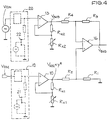
- FIG. 4 shows a tuning circuit according to the invention. This arrangement is essentially fed by two voltage sources.
- the adjustable, variable oscillator tuning voltage V OSZ is applied to the non-inverting input of a first operational amplifier 10 .
- a prescaler 19 can be installed between the oscillator tuning voltage V OSZ and the non-inverting input of the operational amplifier 10 . This alternative is shown in dashed lines in the figure.
- the prescaler 19 consists of two resistors, a field-effect transistor 21, also called an FET, and a DC voltage source.
- the DC voltage source lies between the gate and source connection of the FET 21 .
- a resistor is connected to the drain terminal, which is connected on the one hand to the oscillator tuning voltage V OSZ via another resistor and on the other hand to the non-inverting input of the first operational amplifier 10 .
- the inverting input of the first operational amplifier 10 is connected to a voltage divider, the voltage divider consists of two resistors R N1 , R X1 .
- One resistor R N1 is connected to the output of operational amplifier 10 , to the inverting input of operational amplifier 10 and to the other variable resistor R X1 , which is connected to ground on the one hand and to the inverting input of operational amplifier 10 on the other hand. This amplifies the voltage V OSZ applied to the non-inverting input.
- This amplified voltage V OSZ ⁇ Y * is applied via a resistor R 2 to the non-inverting input of a second operational amplifier 16 .
- This resistor R 2 is in turn connected to another resistor R 1 , which is also applied to the non-inverting input of the second operational amplifier 16 and to ground.
- a fixed input voltage V IN is applied to the non-inverting input of a third operational amplifier 13 .
- a prescaler 20 can be installed between the fixed input voltage V IN and the non-inverting input. This alternative is shown in dashed lines in the figure.
- the prescaler 20 consists of two resistors: a field effect transistor 22, also called an FET, and a DC voltage source.
- the DC voltage source is located between the gate and source connection of the FET 20 .
- a resistor is connected to the drain terminal, which is connected on the one hand to the fixed input voltage V IN via another resistor and on the other hand to the non-inverting input of the third operational amplifier 13 .
- the inverting input of the third operational amplifier 13 is connected to a voltage divider, as is customary in an amplifier circuit, the voltage divider consists of two resistors R X2 , R N2 .
- One resistor R N2 is connected to the output of the third operational amplifier 13 , to the inverting input of the third operational amplifier 13 and to the other variable resistor R X2 , which is connected to ground on the one hand and to the inverting input of the third operational amplifier 13 on the other hand.
- This voltage V OUT reaches the inverting input of the second operational amplifier 16 via a resistor R 4 .
- This resistor R 4 is connected to another resistor R 3 , this resistor R 3 is also connected to the inverting input of the second operational amplifier 16 and to the output of the second operational amplifier 16 .
- the voltage V END is then present at the output of the second operational amplifier 16 .
- the task of such a circuit is that the amplifier 10 amplifies the input voltage in the application example the oscillator tuning voltage V OSZ or a voltage dependent thereon by the factor Y * .
- the gain can be set linearly in a specified step size and resolution.
- the linearity can be achieved, for example, by connecting the resistor R N1 with binary graded values from the resistor R X1 .
- the variable resistor R X1 then actually consists of several resistors connected in parallel, which can be connected depending on the level of the desired resistance value.
- the gain factor Y * can be set linearly.
- the other operational amplifier 13 supplies a linearly adjustable output voltage (DA converter).
- DA converter linearly adjustable output voltage
- the predetermined X and Y coefficients can be set with this circuit.
Landscapes
- Engineering & Computer Science (AREA)
- Computer Hardware Design (AREA)
- Microelectronics & Electronic Packaging (AREA)
- Stabilization Of Oscillater, Synchronisation, Frequency Synthesizers (AREA)
- Superheterodyne Receivers (AREA)
- Television Receiver Circuits (AREA)
Applications Claiming Priority (2)
| Application Number | Priority Date | Filing Date | Title |
|---|---|---|---|
| DE19741325 | 1997-09-19 | ||
| DE19741325A DE19741325C2 (de) | 1997-09-19 | 1997-09-19 | Verfahren zum Abgleich eines mehrstufigen selektiven Verstärkers |
Publications (2)
| Publication Number | Publication Date |
|---|---|
| EP0903852A1 true EP0903852A1 (fr) | 1999-03-24 |
| EP0903852B1 EP0903852B1 (fr) | 2004-02-18 |
Family
ID=7842910
Family Applications (1)
| Application Number | Title | Priority Date | Filing Date |
|---|---|---|---|
| EP98116588A Expired - Lifetime EP0903852B1 (fr) | 1997-09-19 | 1998-09-02 | Procédé d' accord d' un amplificateur sélectif à plusieurs étages |
Country Status (4)
| Country | Link |
|---|---|
| US (1) | US6188970B1 (fr) |
| EP (1) | EP0903852B1 (fr) |
| JP (1) | JPH11225084A (fr) |
| DE (2) | DE19741325C2 (fr) |
Families Citing this family (6)
| Publication number | Priority date | Publication date | Assignee | Title |
|---|---|---|---|---|
| US6411343B1 (en) | 1998-05-21 | 2002-06-25 | E Guide, Inc. | Smart-channel: learning-capable television channel changing apparatus, system and method |
| US6535722B1 (en) * | 1998-07-09 | 2003-03-18 | Sarnoff Corporation | Television tuner employing micro-electro-mechanically-switched tuning matrix |
| DE19957365A1 (de) * | 1999-11-29 | 2001-05-31 | Thomson Brandt Gmbh | Verbesserung des Videofrequenzgangs |
| JP3974497B2 (ja) * | 2002-10-29 | 2007-09-12 | 新潟精密株式会社 | 受信機、デジタル−アナログ変換器および同調回路 |
| US7236756B2 (en) * | 2002-12-13 | 2007-06-26 | Freescale Semiconductors, Inc. | Tuning signal generator and method thereof |
| CN116930301A (zh) * | 2023-03-22 | 2023-10-24 | 中法渤海地质服务有限公司 | 一种用于检测c6-c8的电子倍增器的校正方法 |
Citations (4)
| Publication number | Priority date | Publication date | Assignee | Title |
|---|---|---|---|---|
| EP0601743A1 (fr) * | 1992-12-10 | 1994-06-15 | Nokia Mobile Phones Ltd. | L'accord d'un récepteur radio |
| EP0624949A1 (fr) * | 1993-05-12 | 1994-11-17 | Laboratoires D'electronique Philips S.A.S. | Appareil comprenant un circuit ayant une réponse entrée/sortie contrôlable par un signal de commande et procédé d'approximation |
| US5428829A (en) * | 1992-09-28 | 1995-06-27 | Delco Electronics Corporation | Method and apparatus for tuning and aligning an FM receiver |
| EP0766391A1 (fr) * | 1995-09-29 | 1997-04-02 | Sanyo Electric Co., Ltd. | Récepteur radio |
Family Cites Families (4)
| Publication number | Priority date | Publication date | Assignee | Title |
|---|---|---|---|---|
| DE2524171C2 (de) * | 1975-05-31 | 1984-11-08 | Telefunken electronic GmbH, 7100 Heilbronn | Abstimmschaltung |
| FR2486332B1 (fr) * | 1980-07-04 | 1986-05-30 | Thomson Brandt | Dispositif de reglage du point de fonctionnement d'un circuit electronique comportant plusieurs elements variables, notamment en television par satellite |
| DE3332206A1 (de) * | 1983-09-07 | 1985-04-25 | Grundig E.M.V. Elektro-Mechanische Versuchsanstalt Max Grundig holländ. Stiftung & Co KG, 8510 Fürth | Verfahren zum abgleich eines mehrstufigen selektiven verstaerkers und anordnung zur durchfuehrung des verfahrens |
| DE3930361C2 (de) | 1989-09-12 | 1993-11-04 | Simon Desanta | Stuhl, insbesondere buerostuhl |
-
1997
- 1997-09-19 DE DE19741325A patent/DE19741325C2/de not_active Expired - Fee Related
-
1998
- 1998-09-02 DE DE59810779T patent/DE59810779D1/de not_active Expired - Lifetime
- 1998-09-02 JP JP10285816A patent/JPH11225084A/ja active Pending
- 1998-09-02 EP EP98116588A patent/EP0903852B1/fr not_active Expired - Lifetime
- 1998-09-17 US US09/156,366 patent/US6188970B1/en not_active Expired - Lifetime
Patent Citations (4)
| Publication number | Priority date | Publication date | Assignee | Title |
|---|---|---|---|---|
| US5428829A (en) * | 1992-09-28 | 1995-06-27 | Delco Electronics Corporation | Method and apparatus for tuning and aligning an FM receiver |
| EP0601743A1 (fr) * | 1992-12-10 | 1994-06-15 | Nokia Mobile Phones Ltd. | L'accord d'un récepteur radio |
| EP0624949A1 (fr) * | 1993-05-12 | 1994-11-17 | Laboratoires D'electronique Philips S.A.S. | Appareil comprenant un circuit ayant une réponse entrée/sortie contrôlable par un signal de commande et procédé d'approximation |
| EP0766391A1 (fr) * | 1995-09-29 | 1997-04-02 | Sanyo Electric Co., Ltd. | Récepteur radio |
Also Published As
| Publication number | Publication date |
|---|---|
| DE19741325A1 (de) | 1999-04-08 |
| US6188970B1 (en) | 2001-02-13 |
| DE19741325C2 (de) | 1999-10-07 |
| JPH11225084A (ja) | 1999-08-17 |
| DE59810779D1 (de) | 2004-03-25 |
| EP0903852B1 (fr) | 2004-02-18 |
Similar Documents
| Publication | Publication Date | Title |
|---|---|---|
| DE2622594C2 (fr) | ||
| DE3234236C2 (de) | Abstimmsystem | |
| DE3303711C2 (de) | Abstimmeinheit für Geräte der Nachrichtentechnik | |
| EP1069680A2 (fr) | Circuit d' accord avec au moins une première et une deuxième bande de fréquence | |
| DE2728600C2 (de) | Signalempfänger mit Frequenzabstimmvorrichtung | |
| DE3406150C2 (fr) | ||
| DE3332206A1 (de) | Verfahren zum abgleich eines mehrstufigen selektiven verstaerkers und anordnung zur durchfuehrung des verfahrens | |
| DE2803028C2 (de) | Voreinstellbarer Tuner | |
| DE19734265C2 (de) | Fernsehtuner | |
| DE3036351A1 (de) | Suchabstimmsystem mit direkt adressierender kanalwahl | |
| EP0623992A2 (fr) | Oscillateur | |
| EP0903852B1 (fr) | Procédé d' accord d' un amplificateur sélectif à plusieurs étages | |
| DE3411241A1 (de) | Gleichlaufschaltung fuer tuner unter verwendung eines prom-speichers | |
| DE2501818A1 (de) | Ueberlagerungsoszillator fuer kanalwaehler | |
| DE2718746C2 (de) | Kanalwahlvorrichtung | |
| DE2403162C2 (de) | Automatischer Frequenznachstimmkreis | |
| DE19650524A1 (de) | Doppelabstimmschaltung für TV-Tuner | |
| DE2522055A1 (de) | Elektronisches kanalwahlsystem, insbesondere fuer fernsehgeraete | |
| DE3609349A1 (de) | Superhet-fernsehabstimmvorrichtung | |
| DE2709751A1 (de) | Tuner | |
| DE2744213C2 (de) | Verfahren zur Abstimmung eines innerhalb eines Schaltungsverbundes im Signalweg angeordneten mehrkreisigen Bandfilters und Anordnung zur Durchführung des Verfahrens | |
| DE2814429A1 (de) | Empfaengerschaltung mit einem frequenzsynthetisator in nachrichtentechnischen empfangsgeraeten | |
| DE69423539T3 (de) | Abstimmeinrichtung für einen Radiowellenempfänger mit in Drucktechnik ausgeführten Wicklungen | |
| EP0252272B1 (fr) | Récepteur haute fréquence avec indication numérique de la fréquence de réception | |
| WO1995006359A1 (fr) | Systeme asservi en phase |
Legal Events
| Date | Code | Title | Description |
|---|---|---|---|
| PUAI | Public reference made under article 153(3) epc to a published international application that has entered the european phase |
Free format text: ORIGINAL CODE: 0009012 |
|
| AK | Designated contracting states |
Kind code of ref document: A1 Designated state(s): DE FR GB IT |
|
| AX | Request for extension of the european patent |
Free format text: AL;LT;LV;MK;RO;SI |
|
| 17P | Request for examination filed |
Effective date: 19990804 |
|
| AKX | Designation fees paid |
Free format text: DE FR GB IT |
|
| RAP1 | Party data changed (applicant data changed or rights of an application transferred) |
Owner name: BECKER GMBH Owner name: ATMEL GERMANY GMBH |
|
| 17Q | First examination report despatched |
Effective date: 20020827 |
|
| GRAP | Despatch of communication of intention to grant a patent |
Free format text: ORIGINAL CODE: EPIDOSNIGR1 |
|
| GRAS | Grant fee paid |
Free format text: ORIGINAL CODE: EPIDOSNIGR3 |
|
| GRAA | (expected) grant |
Free format text: ORIGINAL CODE: 0009210 |
|
| AK | Designated contracting states |
Kind code of ref document: B1 Designated state(s): DE FR GB IT |
|
| REG | Reference to a national code |
Ref country code: GB Ref legal event code: FG4D Free format text: NOT ENGLISH |
|
| REF | Corresponds to: |
Ref document number: 59810779 Country of ref document: DE Date of ref document: 20040325 Kind code of ref document: P |
|
| GBT | Gb: translation of ep patent filed (gb section 77(6)(a)/1977) |
Effective date: 20040623 |
|
| ET | Fr: translation filed | ||
| PLBE | No opposition filed within time limit |
Free format text: ORIGINAL CODE: 0009261 |
|
| STAA | Information on the status of an ep patent application or granted ep patent |
Free format text: STATUS: NO OPPOSITION FILED WITHIN TIME LIMIT |
|
| 26N | No opposition filed |
Effective date: 20041119 |
|
| PGFP | Annual fee paid to national office [announced via postgrant information from national office to epo] |
Ref country code: IT Payment date: 20080924 Year of fee payment: 11 Ref country code: FR Payment date: 20080912 Year of fee payment: 11 |
|
| PGFP | Annual fee paid to national office [announced via postgrant information from national office to epo] |
Ref country code: GB Payment date: 20080918 Year of fee payment: 11 |
|
| GBPC | Gb: european patent ceased through non-payment of renewal fee |
Effective date: 20090902 |
|
| REG | Reference to a national code |
Ref country code: FR Ref legal event code: ST Effective date: 20100531 |
|
| PG25 | Lapsed in a contracting state [announced via postgrant information from national office to epo] |
Ref country code: FR Free format text: LAPSE BECAUSE OF NON-PAYMENT OF DUE FEES Effective date: 20090930 |
|
| PG25 | Lapsed in a contracting state [announced via postgrant information from national office to epo] |
Ref country code: GB Free format text: LAPSE BECAUSE OF NON-PAYMENT OF DUE FEES Effective date: 20090902 |
|
| PG25 | Lapsed in a contracting state [announced via postgrant information from national office to epo] |
Ref country code: IT Free format text: LAPSE BECAUSE OF NON-PAYMENT OF DUE FEES Effective date: 20090902 |
|
| PGFP | Annual fee paid to national office [announced via postgrant information from national office to epo] |
Ref country code: DE Payment date: 20170821 Year of fee payment: 20 |
|
| REG | Reference to a national code |
Ref country code: DE Ref legal event code: R071 Ref document number: 59810779 Country of ref document: DE |