EP0905761A2 - Procédé de fabrication d'un transistor à effet de champ - Google Patents
Procédé de fabrication d'un transistor à effet de champ Download PDFInfo
- Publication number
- EP0905761A2 EP0905761A2 EP98306902A EP98306902A EP0905761A2 EP 0905761 A2 EP0905761 A2 EP 0905761A2 EP 98306902 A EP98306902 A EP 98306902A EP 98306902 A EP98306902 A EP 98306902A EP 0905761 A2 EP0905761 A2 EP 0905761A2
- Authority
- EP
- European Patent Office
- Prior art keywords
- region
- gate
- forming
- layer
- dielectric layer
- Prior art date
- Legal status (The legal status is an assumption and is not a legal conclusion. Google has not performed a legal analysis and makes no representation as to the accuracy of the status listed.)
- Withdrawn
Links
Images




Classifications
-
- H—ELECTRICITY
- H10—SEMICONDUCTOR DEVICES; ELECTRIC SOLID-STATE DEVICES NOT OTHERWISE PROVIDED FOR
- H10D—INORGANIC ELECTRIC SEMICONDUCTOR DEVICES
- H10D30/00—Field-effect transistors [FET]
- H10D30/01—Manufacture or treatment
- H10D30/021—Manufacture or treatment of FETs having insulated gates [IGFET]
- H10D30/0223—Manufacture or treatment of FETs having insulated gates [IGFET] having source and drain regions or source and drain extensions self-aligned to sides of the gate
- H10D30/0225—Manufacture or treatment of FETs having insulated gates [IGFET] having source and drain regions or source and drain extensions self-aligned to sides of the gate using an initial gate mask complementary to the prospective gate location, e.g. using dummy source and drain electrodes
-
- H—ELECTRICITY
- H10—SEMICONDUCTOR DEVICES; ELECTRIC SOLID-STATE DEVICES NOT OTHERWISE PROVIDED FOR
- H10D—INORGANIC ELECTRIC SEMICONDUCTOR DEVICES
- H10D30/00—Field-effect transistors [FET]
- H10D30/01—Manufacture or treatment
- H10D30/021—Manufacture or treatment of FETs having insulated gates [IGFET]
- H10D30/0223—Manufacture or treatment of FETs having insulated gates [IGFET] having source and drain regions or source and drain extensions self-aligned to sides of the gate
-
- H—ELECTRICITY
- H10—SEMICONDUCTOR DEVICES; ELECTRIC SOLID-STATE DEVICES NOT OTHERWISE PROVIDED FOR
- H10D—INORGANIC ELECTRIC SEMICONDUCTOR DEVICES
- H10D30/00—Field-effect transistors [FET]
- H10D30/01—Manufacture or treatment
- H10D30/021—Manufacture or treatment of FETs having insulated gates [IGFET]
- H10D30/031—Manufacture or treatment of FETs having insulated gates [IGFET] of thin-film transistors [TFT]
- H10D30/0321—Manufacture or treatment of FETs having insulated gates [IGFET] of thin-film transistors [TFT] comprising silicon, e.g. amorphous silicon or polysilicon
- H10D30/0323—Manufacture or treatment of FETs having insulated gates [IGFET] of thin-film transistors [TFT] comprising silicon, e.g. amorphous silicon or polysilicon comprising monocrystalline silicon
-
- H—ELECTRICITY
- H10—SEMICONDUCTOR DEVICES; ELECTRIC SOLID-STATE DEVICES NOT OTHERWISE PROVIDED FOR
- H10D—INORGANIC ELECTRIC SEMICONDUCTOR DEVICES
- H10D62/00—Semiconductor bodies, or regions thereof, of devices having potential barriers
- H10D62/10—Shapes, relative sizes or dispositions of the regions of the semiconductor bodies; Shapes of the semiconductor bodies
- H10D62/17—Semiconductor regions connected to electrodes not carrying current to be rectified, amplified or switched, e.g. channel regions
- H10D62/351—Substrate regions of field-effect devices
- H10D62/357—Substrate regions of field-effect devices of FETs
- H10D62/364—Substrate regions of field-effect devices of FETs of IGFETs
- H10D62/371—Inactive supplementary semiconductor regions, e.g. for preventing punch-through, improving capacity effect or leakage current
-
- H—ELECTRICITY
- H10—SEMICONDUCTOR DEVICES; ELECTRIC SOLID-STATE DEVICES NOT OTHERWISE PROVIDED FOR
- H10D—INORGANIC ELECTRIC SEMICONDUCTOR DEVICES
- H10D64/00—Electrodes of devices having potential barriers
- H10D64/01—Manufacture or treatment
- H10D64/017—Manufacture or treatment using dummy gates in processes wherein at least parts of the final gates are self-aligned to the dummy gates, i.e. replacement gate processes
-
- H—ELECTRICITY
- H10—SEMICONDUCTOR DEVICES; ELECTRIC SOLID-STATE DEVICES NOT OTHERWISE PROVIDED FOR
- H10W—GENERIC PACKAGES, INTERCONNECTIONS, CONNECTORS OR OTHER CONSTRUCTIONAL DETAILS OF DEVICES COVERED BY CLASS H10
- H10W10/00—Isolation regions in semiconductor bodies between components of integrated devices
- H10W10/01—Manufacture or treatment
- H10W10/011—Manufacture or treatment of isolation regions comprising dielectric materials
- H10W10/018—Manufacture or treatment of isolation regions comprising dielectric materials using selective deposition of crystalline silicon, e.g. using epitaxial growth of silicon
-
- H—ELECTRICITY
- H10—SEMICONDUCTOR DEVICES; ELECTRIC SOLID-STATE DEVICES NOT OTHERWISE PROVIDED FOR
- H10W—GENERIC PACKAGES, INTERCONNECTIONS, CONNECTORS OR OTHER CONSTRUCTIONAL DETAILS OF DEVICES COVERED BY CLASS H10
- H10W10/00—Isolation regions in semiconductor bodies between components of integrated devices
- H10W10/10—Isolation regions comprising dielectric materials
-
- H—ELECTRICITY
- H10—SEMICONDUCTOR DEVICES; ELECTRIC SOLID-STATE DEVICES NOT OTHERWISE PROVIDED FOR
- H10D—INORGANIC ELECTRIC SEMICONDUCTOR DEVICES
- H10D30/00—Field-effect transistors [FET]
- H10D30/01—Manufacture or treatment
- H10D30/021—Manufacture or treatment of FETs having insulated gates [IGFET]
- H10D30/0217—Manufacture or treatment of FETs having insulated gates [IGFET] forming self-aligned punch-through stoppers or threshold implants under gate regions
-
- H—ELECTRICITY
- H10—SEMICONDUCTOR DEVICES; ELECTRIC SOLID-STATE DEVICES NOT OTHERWISE PROVIDED FOR
- H10D—INORGANIC ELECTRIC SEMICONDUCTOR DEVICES
- H10D30/00—Field-effect transistors [FET]
- H10D30/60—Insulated-gate field-effect transistors [IGFET]
- H10D30/67—Thin-film transistors [TFT]
- H10D30/6729—Thin-film transistors [TFT] characterised by the electrodes
- H10D30/673—Thin-film transistors [TFT] characterised by the electrodes characterised by the shapes, relative sizes or dispositions of the gate electrodes
- H10D30/6733—Multi-gate TFTs
Definitions
- This invention relates generally to the fabrication of semiconductor devices, and more particularly, to the fabrication of integrated circuit semiconductor devices which have a buried, doped region such as a back gate region.
- the doped region is aligned with respect to selected elements of the component.
- This technique provides an implanted and aligned back gate, but the back gate typically extends in the region under the source drain terminal providing undesirable capacitance therebetween and increasing the opportunity for leakage current between the back gate region and the source/drain terminals.
- the extension of the punch-through implant region is in part due to the straggle of the implanted ions, but this extension is exacerbated by diffusion during the gate oxidation and during the source-drain anneal.
- SOI silicon-on-insulator
- the aforementioned and other features are accomplished, by fabricating appropriately doped regions for source/drain terminals in the vicinity of a region shadowed by a disposable gate terminal.
- the disposable gate region and the source/drain regions that extend from the disposable gate terminal are covered with a protective material.
- the protective material and the disposable gate terminal are planarized generally parallel to the substrate.
- the disposable gate material is then removed leaving an aperture in the protective material.
- An ion beam is used to implant a punch-through implant region beneath a conducting region, the conducting region electrically coupling the source/drain terminals.
- the aperture is filled with a conducting material, that forms a transistor gate element.
- the punch-through implant region is directly beneath the gate terminal and is aligned therewith.
- the punch-through implant region can be further centered by forming sidewall regions on the walls of the aperture resulting from the removal of the disposable gate.
- a similar procedure can be performed on a silicon-on-insulator structure to provide an aligned, doped region under the gate terminal.
- a disposable gate 101 formed from a material such as polysilicon or silicon nitride, is formed over a gate oxide layer 102, the gate oxide layer formed on a substrate 100.
- the substrate 100 and disposable gate 101 have an ion beam 109 applied thereto.
- the ion beam 109 implants ions in source/drain electrode regions 103 in the substrate 100.
- the source/drain regions 103 are formed in portions of the substrate not shadowed by the disposable gate 101.
- a sidewall structure can be formed on the disposable gate (not shown) further to space apart the source and drain implant regions.
- Arsenic and phosphorous ions can be used to form the electrodes in n-channel field effect transistors, while boron and boron fluoride ions can be used to form electrodes in p-channel field effect transistors.
- an anneal step is performed.
- gate oxide 100 and the disposable gate 101 have a dielectric material 104 applied thereto as shown in Fig. 1C.
- the dielectric material 104 as well as the disposable gate 101 are planarized (i.e., a surface generally parallel with the substrate 100 is formed) with the result that a top portion of the disposable gate 101 is exposed.
- the exposed disposable gate 101 is removed leaving an aperture 105 as shown in Fig. 1E.
- the resulting structure is exposed to ion beam 108.
- the ion beam 108 results in formation of the channel implant 106 and in the formation of a local well (punch-through implant) region 107.
- the initial gate oxide can be removed and the final gate oxide formed.
- a layer of gate material 110 e.g., titanium nitride
- the gate material is removed from the surface of the dielectric material 104 leaving only the conducting material 110 now in the aperture 105.
- the gate of the transistor component is now exposed and is available for coupling to conducting leads. The conducting leads applying control signals to the gate element of the transistor component.
- a technique for providing a more localized back gate is shown. This procedure can replace the process step(s) illustrated in Fig. 1E.
- Fig. 2A after the channel implant, sidewalls 201 are formed on walls of the aperature 105 formed by the removal of the disposable gate 101 (cf. Fig. 1F). Ion beam 202 then forms back gate region 207 in Fig. 2B.
- Fig. 2C the sidewalls 201 are removed. The process then continues as shown in Fig. 1F wherein a gate electrode for the transistor component is formed.
- a technique is illustrated for insuring that the separation of the back gate region from the source/drain electrodes is maintained for fabrication of a field effect transistor.
- a gate oxide layer 302 is formed on a substrate 300.
- a dielectric layer 304 is formed on gate oxide layer 302.
- the dielectric layer 304 has aperture 320 in a position relative to substrate 300 where the gate structure will eventually be positioned.
- a channel implant 306 is formed under the aperture 320.
- sidewalls 301 are formed on the walls of the aperature 320.
- Ions 305 are applied to the substrate/dielectric combination and a punch-through implant region 307 is formed in the substrate 300.
- the sidewalls 301 are removed and the aperture 320 is filled with a conducting material which will be the gate structure 309.
- Source/drain electrodes 303 are formed in the region having a boundary formed by the shadow of the gate structure 309. The sidewalls 301 cause the back gate rear to be sufficiently far from the boundary gate structure 309 shadow that even diffusion by the source/drain electrodes 303 will not result in contact.
- the dotted lines indicate a second approach to separating the source/drain electrodes 303 from the back gate 307.
- Sidewalls 311 are formed around the gate structure 309 either prior to formation of the source/drain electrodes or after the formation of the source drain electrodes 303. If the sidewalls 311 are formed before the formation of the source/drain electrodes, then the source/drain electrodes 312 can be separated from the back gate 307 without the use of sidewalls 301 (shown in Fig. 3B). Similarly, the sidewalls 311 can be formed after the (relatively more lightly doped) source/drain electrodes 303 are formed. In this process, the source/drain electrodes 312 combine with source drain/electrodes 303 to form the transistor source/drain electrodes.
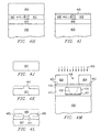
- a prior art process for performing a back contact procedure to provide a buried oxide structure is shown.
- a patterning technique is used to provide a polysilicon structure 401 on a base material 490.
- a dielectric layer (e.g., SiO 2 ) 404 is formed over the polysilicon structure 401 and the base material 490.
- the dielectric layer 404 is then planarized.
- the dielectric layer 404 and the polysilicon structure 401 are then removed from the base material 490.
- the planarized surface of the dielectric layer 404 is bonded to a substrate wafer 400 and a second dielectric layer is formed on the surface of the dielectric layer 404 and the polysilicon structure 401.
- the thickness of the second dielectric layer 430 is reduced in Fig. 4C, resulting in a buried oxide structure.
- a process for providing a buried oxide structure is shown.
- a SiO 2 layer 440 is formed on the surface of a silicon wafer 441.
- an aperture 442 is formed, the aperture extending to the silicon wafer 441, for example, by patterning and etching the dielectric (SiO 2 ) layer 440.
- silicon material 443 is formed in the aperture, for example, by selective epitaxial growth.
- the silicon material 443 and the dielectric layer 440 are planarized and a second dielectric layer is formed on the planarized surface.
- the surface of the second dielectric layer 444 is planarized, the structure including the dielectric layers 440 and 444 and the silicon material 443 is removed from the silicon wafer 441 and the planarized surface of dielectric layer 444 is bonded to substrate wafer 400.
- a third dielectric layer 445 is applied to the surfaces of dielectric layer 440 and silicon material 443. In Fig. 41, the thickness of the third dielectric layer is reduced.
- Fig. 4J two techniques for providing a buried oxide structure from a silicon wafer 441 are shown.
- the surface of the silicon wafer is patterned and etched, for example, to form the structure 443 which will become, after deposition of a dielectric layer, the basis for the buried oxide layer.
- silicon oxide regions 485 are selectively grown on the surface of the silicon wafer 441. After the growth of the silicon oxide regions 485, an additional silicon oxide layer 486 is formed over the silicon oxide regions 485 and the exposed surface of the silicon wafer 441.
- the silicon regions 485 and the silicon region 441' are separated from the remainder of the silicon wafer 441 to form the basis of the buried oxide structure.
- FIG. 4M the process for punch-through implant of ions in a buried oxide structure when the transistor structure is formed on an insulating material substrate (also known as an SOI structure) is shown.
- Buried oxide (BOX) layer 415 is formed on semiconductor substrate 400 as described above.
- the BOX layer 415 includes the silicon region 416.
- Formed on BOX layer 415 is silicon layer 410.
- the silicon layer 410 includes the source/drain electrodes 403.
- a dielectric material 404 Positioned over the silicon layer 410 is a dielectric material 404 which includes an aperture in a position where the gate of the transistor element will be positioned.
- Ions 405 are implanted through the aperture in the dielectric material 404 and change the doping of a portion 420 of doped region 416.
- the region 420 becomes the back gate for the transistor component.
- the aperture in the dielectric material 404, in process steps illustrated in Fig. 1G and Fig. 1H is filled with conducting material and is the gate structure
- Fig. 5 the result of using the process for punch-through implant, described above, is shown in Fig. 5.
- the source/drain structures 503 of the transistor element (having gate structure 510) are shown in a deep well portion 550 of the substrate 500.
- a local well can be provided.
- the local well can provide a region of relatively lower resistivity compared to the deep well in which the transistor element is fabricated.
- individual local wells within a common deep well can be maintained at different voltages.
- a substrate material 600 typically a silicon wafer
- a first gate layer 651 is formed on the gate oxide layer 602, a first gate layer 651 is formed.
- a dielectric (or gate patterning) layer 604 has been formed by a different etch selectivity, e.g., SiO 2 and a gate area 605 is removed from the dielectric layer 604 in Fig. 6A.
- a self-aligned implant of ions 602 to form punch-through implant region 607 is performed.
- Fig. 6B a self-aligned implant of ions 602 to form punch-through implant region 607 is performed.
- a second gate layer 651 is formed over dielectric layer and gate area 605.
- the surface is planarized to provide the device gate.
- the dielectric layer 604 and the first gate layer 650 are removed except where the first gate layer 651 is shadowed by the remaining (i.e., after planarization as shown in Fig. 6C) second gate layer 651.
- a gate oxide layer 702 is formed on a substrate 700.
- a first gate layer 750 is formed on the gate oxide layer 702.
- a disposable gate element 701 is formed, typically by selective etching, over the region wherein the gate electrode will be positioned.
- an ion beam 702 is used to form the source/drain electrodes 703, the disposable gate element 701 preventing the ions 702 from being implanted in the region thereunder.
- a dielectric layer 704 is formed over the disposable gate 701 and the first gate layer 702.
- the dielectric layer 704 is planarized, exposing the disposable gate 701.
- the disposable gate 701 is selectively removed, leaving aperture 705 in the dielectric material 704.
- An ion beam 712 is applied to the device forming the self-aligned punch-through implant region 707.
- a second gate layer 751 is applied to the dielectric layer 704 and into the aperture 705. After planarization in which the dielectric layer 704 is exposed surrounding the second gate layer 751, the dielectric layer 704 and the portion of the first gate layer 750 not protected (shadowed) by the remaining second gate layer 751 are selectively removed.
- the remaining first gate layer 750 and the remaining second gate layer 751 provide the gate structure for the transistor element.
- FIG. 8A a gate oxide layer 802 is formed on substrate 800.
- a gate material layer 803 is formed on the gate oxide layer 802.
- a dielectric layer 804 is formed on gate material layer 803. The dielectric layer 804 is patterned to have an aperture over the portion of the gate material layer 803 which will form the gate electrode of the transistor element.
- An ion beam 812 provides a ion implantation region 807 aligned with the aperture 805.
- a protective layer 820 is applied to the surface of dielectric layer 804 and to the surface of the gate material layer 803 exposed by the aperture 805.
- the dielectric layer 804 and the portion of the protective layer 820 on the surface of dielectric layer 804 are removed.
- the portion of the protective layer 820 on the surface of the gate material layer 803 defined by aperture 805 remains.
- the portion of the gate material layer 803 not shadowed by the remaining protective layer 820 is selectively removed.
- Fig. 8E the portion of the gate oxide 802 not shadowed by the remaining gate material layer 803 is removed.
- the source and drain electrodes 813 of the transistor element are formed by ion implantation outside of the region shadowed by the remaining protective layer 820.
- sidewalls 821 have been added to the structure provided the remaining protective layer 820, the remaining gate material layer 803, and the remaining gate oxide layer 802.
- the source/drain electrodes 813 can be more heavily doped by additional ion implantation.
- the side walls 821 protect the ion implantation region 807 from the heavier doping levels of the extended source/drain electrodes.
- the preferred process results in an aligned back gate for the transistor component fabricated thereby.
- the back gate region prevents punch-through between the electrode regions (103).
- the aligned back gate region can be separated from the electrode regions (103) by processes illustrated in Fig. 2A through Fig. 2C and in Fig. 3A through Fig. 3C.
- the back gate structure serves as a gate structure.
- the back gate structure 416 can be composed of silicon.
- the silicon can be lightly doped oppositely to the self-aligned implant region 420.
- back gate structure 416 can be a lightly-doped p-type region, e.g., with boron, prior to a self aligned n-type implant, e.g., arsenic.
- the back gate structure 416 can optionally be backed with a conducting material to form a backing layer 421, e.g., a metal or a silicide.
- the backing layer 421 is preferably a good implant ion stopping material, e.g., tungsten, resulting in an implant ion accumulation in back gate structure 416.
- a gate oxide is formed, a first gate layer is formed to protect the gate oxide, and the punch-through ion implant is implemented. Following the formation of the punch-through ion implant region, a second gate layer is formed.
- This process of providing two gate layers has the advantage that the ions penetrate a thinner material than would be the situation if the entire gate layer were formed initially. In addition, this process has the advantage that implanted ions are not exposed to the thermal cycle of growing the gate oxide.
- the first and second gate layers have different etch properties, however, this difference in properties is not necessary.
- first and second layer gate materials including polysilicon/metal, metal-1/metal-2, and compounds such as TiN/W can be used.
- Amorphous silicon may be used instead of polysilicon.
- Either or both of the first and second gate layers can be multiple layers of materials, or the first and second gate layers can be formed from the same materials.
- the gate may comprise additional layers.
- a preferred aspect is that the implant process is done through the first layer and the second layer is formed after the implant process. Further, the patterning of the second gate layer can be self-aligned with respect to the ion implantation. In addition, the patterning of the first gate layer may be aligned to the pattern of the second gate layer.
- the punch-through implant region, the local well region, the body contact region, and the back gate region all describe a localized ion implant region.
- polysilicon While the use of polysilicon has been previously proposed for a back-body contact, polysilicon has the disadvantage that diffusion junctions can have a relatively high leakage, increasing the importance of self-alignment of the implanted ion regions.
- Self-alignment of the implanted ion regions is important to reduce the junction capacitance of the device.
Landscapes
- Insulated Gate Type Field-Effect Transistor (AREA)
- Thin Film Transistor (AREA)
Applications Claiming Priority (2)
| Application Number | Priority Date | Filing Date | Title |
|---|---|---|---|
| US5719497P | 1997-08-29 | 1997-08-29 | |
| US57194P | 1997-08-29 |
Publications (2)
| Publication Number | Publication Date |
|---|---|
| EP0905761A2 true EP0905761A2 (fr) | 1999-03-31 |
| EP0905761A3 EP0905761A3 (fr) | 2005-01-26 |
Family
ID=22009078
Family Applications (1)
| Application Number | Title | Priority Date | Filing Date |
|---|---|---|---|
| EP98306902A Withdrawn EP0905761A3 (fr) | 1997-08-29 | 1998-08-27 | Procédé de fabrication d'un transistor à effet de champ |
Country Status (2)
| Country | Link |
|---|---|
| EP (1) | EP0905761A3 (fr) |
| JP (1) | JPH11145475A (fr) |
Cited By (6)
| Publication number | Priority date | Publication date | Assignee | Title |
|---|---|---|---|---|
| WO2000055897A1 (fr) * | 1999-03-17 | 2000-09-21 | Koninklijke Philips Electronics N.V. | Procede de fabrication d'un transistor mis a effet de champ |
| WO2001097290A3 (fr) * | 2000-06-16 | 2002-08-15 | Advanced Micro Devices Inc | Transistor a effet de champ a grille inversee enfouie (bigfet) |
| EP1091414A3 (fr) * | 1999-10-07 | 2005-03-16 | Lucent Technologies Inc. | MOSFET ayant une porte biseautée et sa méthode de fabrication |
| US7314794B2 (en) | 2005-08-08 | 2008-01-01 | International Business Machines Corporation | Low-cost high-performance planar back-gate CMOS |
| CN102842603A (zh) * | 2011-06-23 | 2012-12-26 | 中国科学院微电子研究所 | Mosfet及其制造方法 |
| CN103000671A (zh) * | 2011-09-16 | 2013-03-27 | 中国科学院微电子研究所 | Mosfet及其制造方法 |
Families Citing this family (3)
| Publication number | Priority date | Publication date | Assignee | Title |
|---|---|---|---|---|
| US20060068556A1 (en) | 2004-09-27 | 2006-03-30 | Matsushita Electric Industrial Co., Ltd. | Semiconductor device and method for fabricating the same |
| KR100723246B1 (ko) | 2005-12-27 | 2007-05-29 | 동부일렉트로닉스 주식회사 | 반도체 소자의 제조 방법 |
| JP4618198B2 (ja) * | 2006-06-22 | 2011-01-26 | ソニー株式会社 | 半導体装置の製造方法 |
Family Cites Families (7)
| Publication number | Priority date | Publication date | Assignee | Title |
|---|---|---|---|---|
| JP3029653B2 (ja) * | 1990-09-14 | 2000-04-04 | 株式会社東芝 | 半導体装置の製造方法 |
| JPH07263680A (ja) * | 1994-03-24 | 1995-10-13 | Hitachi Ltd | 半導体装置の製造方法 |
| US5413949A (en) * | 1994-04-26 | 1995-05-09 | United Microelectronics Corporation | Method of making self-aligned MOSFET |
| US5429956A (en) * | 1994-09-30 | 1995-07-04 | United Microelectronics Corporation | Method for fabricating a field effect transistor with a self-aligned anti-punchthrough implant channel |
| US5576227A (en) * | 1994-11-02 | 1996-11-19 | United Microelectronics Corp. | Process for fabricating a recessed gate MOS device |
| US6063675A (en) * | 1996-10-28 | 2000-05-16 | Texas Instruments Incorporated | Method of forming a MOSFET using a disposable gate with a sidewall dielectric |
| US5773348A (en) * | 1997-05-21 | 1998-06-30 | Powerchip Semiconductor Corp. | Method of fabricating a short-channel MOS device |
-
1998
- 1998-08-27 EP EP98306902A patent/EP0905761A3/fr not_active Withdrawn
- 1998-08-28 JP JP10243663A patent/JPH11145475A/ja active Pending
Cited By (11)
| Publication number | Priority date | Publication date | Assignee | Title |
|---|---|---|---|---|
| WO2000055897A1 (fr) * | 1999-03-17 | 2000-09-21 | Koninklijke Philips Electronics N.V. | Procede de fabrication d'un transistor mis a effet de champ |
| US6403426B1 (en) | 1999-03-17 | 2002-06-11 | Koninklijke Philips Electronics N.V. | Method of manufacturing a semiconductor device |
| EP1091414A3 (fr) * | 1999-10-07 | 2005-03-16 | Lucent Technologies Inc. | MOSFET ayant une porte biseautée et sa méthode de fabrication |
| WO2001097290A3 (fr) * | 2000-06-16 | 2002-08-15 | Advanced Micro Devices Inc | Transistor a effet de champ a grille inversee enfouie (bigfet) |
| US7314794B2 (en) | 2005-08-08 | 2008-01-01 | International Business Machines Corporation | Low-cost high-performance planar back-gate CMOS |
| US7750405B2 (en) | 2005-08-08 | 2010-07-06 | International Business Machines Corporation | Low-cost high-performance planar back-gate CMOS |
| CN102842603A (zh) * | 2011-06-23 | 2012-12-26 | 中国科学院微电子研究所 | Mosfet及其制造方法 |
| WO2012174769A1 (fr) * | 2011-06-23 | 2012-12-27 | 中国科学院微电子研究所 | Mosfet et son procédé de fabrication |
| CN102842603B (zh) * | 2011-06-23 | 2015-03-25 | 中国科学院微电子研究所 | Mosfet及其制造方法 |
| CN103000671A (zh) * | 2011-09-16 | 2013-03-27 | 中国科学院微电子研究所 | Mosfet及其制造方法 |
| CN103000671B (zh) * | 2011-09-16 | 2015-07-15 | 中国科学院微电子研究所 | Mosfet及其制造方法 |
Also Published As
| Publication number | Publication date |
|---|---|
| EP0905761A3 (fr) | 2005-01-26 |
| JPH11145475A (ja) | 1999-05-28 |
Similar Documents
| Publication | Publication Date | Title |
|---|---|---|
| JP4110085B2 (ja) | 二重ゲート型電界効果トランジスタの製造方法 | |
| US6391720B1 (en) | Process flow for a performance enhanced MOSFET with self-aligned, recessed channel | |
| US6200866B1 (en) | Use of silicon germanium and other alloys as the replacement gate for the fabrication of MOSFET | |
| US7719033B2 (en) | Semiconductor devices having thin film transistors and methods of fabricating the same | |
| JPH1197693A (ja) | 半導体装置およびその製造方法 | |
| US4845051A (en) | Buried gate JFET | |
| JPH11243210A (ja) | 半導体デバイス及びその製造方法 | |
| US6724049B2 (en) | SOI semiconductor device with insulating film having different properties relative to the buried insulating film | |
| US6998682B2 (en) | Method of forming a partially depleted silicon on insulator (PDSOI) transistor with a pad lock body extension | |
| US20030119264A1 (en) | Method for fabricating highly integrated transistor | |
| US6368903B1 (en) | SOI low capacitance body contact | |
| US7648880B2 (en) | Nitride-encapsulated FET (NNCFET) | |
| KR100393139B1 (ko) | 반도체장치 및 그의 제조방법 | |
| EP0905761A2 (fr) | Procédé de fabrication d'un transistor à effet de champ | |
| US6621118B2 (en) | MOSFET, semiconductor device using the same and production process therefor | |
| KR100259593B1 (ko) | 반도체장치의 제조 방법 | |
| JPH10242297A (ja) | Cmos回路及びその製造方法 | |
| JPS63227059A (ja) | 半導体装置およびその製造方法 | |
| JPH06151842A (ja) | 半導体装置及びその製造方法 | |
| KR100303356B1 (ko) | 더블 게이트 구조를 갖는 에스오아이 소자 및 그 제조방법 | |
| JP2003188186A (ja) | 絶縁ゲート型電界効果トランジスタの製造方法 | |
| JP2004207528A (ja) | 半導体装置及びその製造方法 | |
| JP2003188185A (ja) | 絶縁ゲート型電界効果トランジスタの製造方法 | |
| JPH11204796A (ja) | Mosfetの製造方法 |
Legal Events
| Date | Code | Title | Description |
|---|---|---|---|
| PUAI | Public reference made under article 153(3) epc to a published international application that has entered the european phase |
Free format text: ORIGINAL CODE: 0009012 |
|
| AK | Designated contracting states |
Kind code of ref document: A2 Designated state(s): AT BE CH CY DE DK ES FI FR GB GR IE IT LI LU MC NL PT SE |
|
| AX | Request for extension of the european patent |
Free format text: AL;LT;LV;MK;RO;SI |
|
| PUAL | Search report despatched |
Free format text: ORIGINAL CODE: 0009013 |
|
| AK | Designated contracting states |
Kind code of ref document: A3 Designated state(s): AT BE CH CY DE DK ES FI FR GB GR IE IT LI LU MC NL PT SE |
|
| AX | Request for extension of the european patent |
Extension state: AL LT LV MK RO SI |
|
| AKX | Designation fees paid | ||
| REG | Reference to a national code |
Ref country code: DE Ref legal event code: 8566 |
|
| STAA | Information on the status of an ep patent application or granted ep patent |
Free format text: STATUS: THE APPLICATION IS DEEMED TO BE WITHDRAWN |
|
| 18D | Application deemed to be withdrawn |
Effective date: 20050727 |