EP0905897B1 - Komparatoranordnung mit Schalthysterese - Google Patents
Komparatoranordnung mit Schalthysterese Download PDFInfo
- Publication number
- EP0905897B1 EP0905897B1 EP98116120A EP98116120A EP0905897B1 EP 0905897 B1 EP0905897 B1 EP 0905897B1 EP 98116120 A EP98116120 A EP 98116120A EP 98116120 A EP98116120 A EP 98116120A EP 0905897 B1 EP0905897 B1 EP 0905897B1
- Authority
- EP
- European Patent Office
- Prior art keywords
- comparator
- current
- control
- signal
- arrangement according
- Prior art date
- Legal status (The legal status is an assumption and is not a legal conclusion. Google has not performed a legal analysis and makes no representation as to the accuracy of the status listed.)
- Expired - Lifetime
Links
- 238000004519 manufacturing process Methods 0.000 description 5
- 230000000052 comparative effect Effects 0.000 description 3
- 230000008878 coupling Effects 0.000 description 3
- 238000010168 coupling process Methods 0.000 description 3
- 238000005859 coupling reaction Methods 0.000 description 3
- 230000001419 dependent effect Effects 0.000 description 3
- 238000010586 diagram Methods 0.000 description 3
- 230000007704 transition Effects 0.000 description 2
- 230000000295 complement effect Effects 0.000 description 1
- 238000010276 construction Methods 0.000 description 1
- 238000011161 development Methods 0.000 description 1
- 230000018109 developmental process Effects 0.000 description 1
- 238000005516 engineering process Methods 0.000 description 1
- 230000002349 favourable effect Effects 0.000 description 1
- 238000007667 floating Methods 0.000 description 1
Images
Classifications
-
- H—ELECTRICITY
- H03—ELECTRONIC CIRCUITRY
- H03K—PULSE TECHNIQUE
- H03K5/00—Manipulating of pulses not covered by one of the other main groups of this subclass
- H03K5/22—Circuits having more than one input and one output for comparing pulses or pulse trains with each other according to input signal characteristics, e.g. slope, integral
- H03K5/24—Circuits having more than one input and one output for comparing pulses or pulse trains with each other according to input signal characteristics, e.g. slope, integral the characteristic being amplitude
- H03K5/2472—Circuits having more than one input and one output for comparing pulses or pulse trains with each other according to input signal characteristics, e.g. slope, integral the characteristic being amplitude using field effect transistors
- H03K5/2481—Circuits having more than one input and one output for comparing pulses or pulse trains with each other according to input signal characteristics, e.g. slope, integral the characteristic being amplitude using field effect transistors with at least one differential stage
Definitions
- the invention relates to a comparator arrangement with switching hysteresis.
- the comparison value is indicated by a Switching threshold of the comparator formed. If the input signal is greater than the comparison value, the binary switches Output signal in a first state; if the input signal is less than the comparison value, the output signal switches in a complementary second state.
- US 5 166 550 is a comparator circuit with a variable Hysteresis described.
- a comparator becomes an input signal as well as a reference signal.
- the hysteresis is caused in that the input signal via switching means an additional voltage is superimposed.
- the additional Voltage is controlled depending on the reference signal.
- the switching means become dependent on the output signal of the comparator controlled.
- US Pat. No. 5,369,319 shows a comparator with hysteresis, which is formed from MOS transistors.
- a differential amplifier of the comparator contains a current source transistor which is controlled by a control circuit to temperature and Compensate for manufacturing fluctuations.
- the current source transistor forms a current mirror with the control circuit.
- the load currents in the comparator branches simulated at the respective switching points of the comparator. Through this Circuit arrangement are said to fluctuate on hysteresis be corrected by a control loop.
- the comparator arrangement provides a largely variable switching hysteresis and means for generating a single reference signal ready.
- the object of the invention is a comparator arrangement to indicate with switching hysteresis, its characteristic Parameters as accurate as possible and as independent as possible from production variations are producible.
- a the switching thresholds of the comparators and those on them related hysteresis each determined by reference voltages.
- a control circuit ensures the compensation of Production variations and temperature influences.
- the switching thresholds and the hysteresis are therefore with high accuracy adjustable.
- To implement the comparative comparators become "unbalanced" comparators with switchable offset uses a small chip area with integrated implementation need.
- the control circuit is for control of comparators required only once, so that a chip area favorable Overall arrangement is obtained.
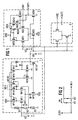
- the comparison comparator 2 shown in FIG. 1 becomes a Input signal IN1 supplied with depending on the current Switching status compared different switching thresholds to generate the output signal OUT1.
- the signal diagram in Figure 2 shows the relationship between input and Output signal of the comparator 2. With increasing input voltage IN1 switches the output signal OUT1 on the Switching threshold VS 'from an L level to an H level. If the input signal IN1 then drops, this happens Switching the output signal OUT1 at the lower one Threshold VS. There is one between the switching thresholds VS, VS ' Hysteresis by setting the switching thresholds around the voltage VH are different from each other.
- the comparator 2 is based on a differential amplifier, which two source-coupled n-channel MOS transistors M21, M22 contains the one formed by a transistor M25 Current source with the reference potential connection of the supply voltage source are connected. Reference potential is mass VSS. At the gate of transistor M21 is a (second) reference voltage VS applied to ground, the corresponds to the lower switching threshold VS in FIG. 2. To the The gate of transistor M22 is the input signal IN1 to apply.
- the current branches of the differential amplifier are open Side of the positive supply potential VDD of the supply voltage with each other via a current mirror M23, M24 coupled.
- the output signal OUT1 of the comparator 2 is on Coupling nodes of the transistors M22, M24 and tapped provided on the output side via a driver stage M27, M28.
- P-channel MOS transistors are one away from the gate marked arrow, with n-channel MOS transistors an arrow pointing towards the gate.
- the load M24 in the output branch of the differential amplifier Comparator 2 is made by connecting transistors in parallel M241, M242 formed.
- a switching transistor M26 connected by the output signal OUT1 is controlled.
- the one as a p-channel MOS transistor executed switch M26 is at an H level of Output signal OUT1 blocked, switched to an L level.
- the load M24 is therefore in the former switching state formed only by transistor M241, in the latter switching state by connecting the transistors M241 in parallel, M242. This asymmetrical construction of the differential amplifier of the comparator 2 will be offset by the output signal OUT1 controlled switchable.
- Offset voltage of a comparator is the voltage on the input side is to be applied so that the output signal is floating is in balance, i.e. is at the switching threshold.
- the Signal diagram is the offset the shift of the switching threshold compared to the zero point of the differential voltage to the Inputs of the comparator. The offset is therefore the Switching threshold of the comparator set.
- For level transitions of the input signal IN1 from H to L is only for the load M24 the transistor M241 effective, so that the switching threshold at lower value VS.
- transitions of the input signal IN1 from L to H is the parallel connection for the load M24 of the transistors M241, M242 effective, so that the switching threshold at the higher value VS '.
- a control circuit 1 which generates a control signal VB.
- the control signal VB is the Gate of the current source transistor M25 is supplied to adjust its current.
- the signal VB the reference potential side current source transistor M28 controlled in the output driver current path of switching stage 2.
- the control circuit includes a differential amplifier source-coupled transistors M11, M12. Between the the Input connections of the gate connections forming the differential amplifier of the transistors M11, M12 is the (first) reference voltage VH created by which the hysteresis is determined. The gate of transistor M11 is also through the (second) reference voltage related to reference potential VS, which defines the lower switching threshold of the comparator 2, biased. On the side of the supply potential VDD is in the differential amplifier branch containing the transistor M12 as a load M14, a parallel connection consisting of transistors M141, M142 switched, which are controlled by the same Gate connections are interconnected. In the other, the Differential amplifier branch containing transistor M11 a load formed by a transistor M13.
- the burdens M13, M14 are different, so that the differential amplifier the control circuit 1 is asymmetrical.
- the differential amplifier therefore has an offset.
- the offset is in his absolute height adjustable by changing the current IB, that at the coupling node of the source connections of the transistors M11, M12 is stamped. This is done by a transistor M15 formed, switched to reference potential power source.
- the current IB is set such that the offset of the Differential amplifier on its input reference voltage VH is settled. This means that the difference from offset and reference voltage VH becomes as small as possible; apart from a proportional control error that is negligible in practice is the actual offset of the amplifier stage equal to the specification by the reference signal VH on.
- the control loop contains a (first) current path from transistor M17, M19, the transistor M17 with a current mirror to the load transistor M13 of the differential amplifier forms.
- One on the side of the supply potential VDD switched transistor M16 becomes equal to the other load M14 of the differential amplifier controlled by their gate connections are interconnected.
- Transistor M16 is in one (Second) current path included. This is via a reference potential side Current mirror M18, M19 in the first Current path coupled.
- a correction current IK is tapped from M17, M19 of the first current path, the compared to the current direction shown be positive or negative during regulation can.
- the current source transistor 15 of the differential amplifier finally it is controlled via a current mirror M15, M110.
- the transistor M110 is in a (further) current path contain a reference current formed by a current source IR leads.
- the correction current is in this current path IK coupled.
- This control loop causes due to the asymmetrical dimensioning of the load elements of the differential amplifier formed equal to the default with the reference voltage VH.
- the control voltage controlling the current source transistor M15 VB serves as the output signal of the control circuit 1.
- the control voltage VB is used to control a corresponding current source transistor used in the comparator 2, so that Offset voltage depending on the control circuit 1 setting offset voltage is determined. If the load M24 of the comparator 2 through the parallel connection of the transistors M241, M242 is formed and provided that corresponding elements of the differential amplifier Control circuit 1 and the comparator 2 relative to each other the differential amplifiers have the same dimensions both circuit parts 1, 2 have the same offset.
- the offset of the comparator 2 and thus its hysteresis are therefore by the control circuit 1 to the desired value VH regardless of any manufacturing or temperature-related Variations adjustable.
- the comparator 2 are further comparators with respect to the reference voltage VS and the control voltage VB in parallel switchable, of which a comparator 3 is shown as an example is. If the transistors of the other comparators 3 is the same as the transistors M21, M22, M23, M24, M25 of the differential amplifier of the comparator 2 are dimensioned there is also the same offset, exactly the specification corresponds to the reference signal VH. Because the control circuit 1 is only required once, a large number are similar Comparators with the same, precisely defined switching points realizable with little effort and space.
- the reference voltages VH, VS are expediently determined by means of a voltage divider R1, R2, R3 generated.
- the voltage divider is connected between the supply voltage VDD, VSS and has a resistance R2 which is between the Gate connections of the transistors M11, M12 is connected.
- Reference potential side is the resistor R2 across another Resistor R3 connected; is on the supply potential side it via a resistor R1 to the connection for the supply potential VDD coupled.
- the reference voltage VS drops on the series connection of the resistors R2, R3.
- the reference signals VS, VH are precisely specified.
Landscapes
- Physics & Mathematics (AREA)
- Nonlinear Science (AREA)
- Manipulation Of Pulses (AREA)
- Measurement Of Current Or Voltage (AREA)
Description
- Figur 1
- eine Realisierung der Komparatoranordnung in MOS-Schaltungstechnik und
- Figur 2
- ein Signaldiagramm für einen Vergleichskomparator.
Claims (9)
- Komparatoranordnung mit Schalthysterese umfassend:eine Regelschaltung (1) zur Erzeugung eines Steuersignals (VB), dieeinen Differenzverstärker (M11, ..., M15) enthält, mit einer Differenzverstärkerstufe (M11, M12), zwei Lastelementen (M13, M14) und einer gemeinsamen Stromquelle (M15) zum kontinuierlichen Steuern des Offsets,zwischen dessen Eingangssignalanschlüssen Mittel (R2) zur Erzeugung eines ersten Referenzsignals (VH), das ein Maß für die durch die Hysterese gebildete Verschiebung von Schaltschwellen der Komparatoranordnung ist, geschaltet sind,dessen einer Eingangssignalanschluß gegenüber einem Bezugspotentialanschluß (VSS) mit einem Mittel (R2, R3) zur Erzeugung eines zweiten Referenzsignals (VS), das ein Maß für eine der Schaltschwellen der Komparatoranordnung ist, verbunden ist, undin dem das Steuersignal (VB) auf den Steuereingang der Stromquelle (M15) rückgekoppelt wird, um den Offset zu steuern, so daß der Offset auf das erste Referenzsignal (VH) ausgeregelt wird, undeinen Komparator (2),der einen Offset aufweist, der abhängig von einem Ausgangssignal (OUT1) des Komparators (2) schaltbar gesteuert wird und vom Steuersignal (VB) kontinuierlich gesteuert wird,der einen Eingangsanschluß aufweist, der an die Mittel (R2, R3) zur Erzeugung des zweiten Referenzsignals (VS) angeschlossen ist, undder einen weiteren Eingangsanschluß für ein Eingangssignal (IN1) aufweist.
- Komparatoranordnung nach Anspruch 1,
dadurch gekennzeichnet, daß
der Komparator (2) und die Regelschaltung (1) jeweils einen Differenzverstärker (M11, ..., M15; M21, ..., M25) mit einer auf der Seite des Bezugspotentialanschlusses (VSS) angeordneter Stromquelle (M15; M25) umfassen, deren Stromstärke vom Steuersignal (VB) gesteuert wird. - Komparatoranordnung nach Anspruch 2,
dadurch gekennzeichnet, daß
einer der Zweige (M11, M13) des Differenzverstärkers der Regelschaltung (1) versorgungspotentialseitig einen Stromspiegel (M13, M17) mit einem ersten Strompfad (M17, M19) bildet, daß ein Lastelement (M14) des anderen der Zweige (M12, M14) des Differenzverstärkers der Regelschaltung (1) gleich einem versorgungspotentialseitigen Lastelement (M16) in einem zweiten Strompfad (M16, M18) gesteuert wird, und daß der zweite Strompfad (M16, M18) einen bezugspotentialseitigen Stromspiegel (M18, M19) mit dem ersten Strompfad (M17, M19) bildet. - Komparatoranordnung nach Anspruch 3,
dadurch gekennzeichnet, daß
die auf der Seite des Bezugspotentialanschlusses (VSS) angeordnete Stromquelle (M15) des Differenzverstärkers der Regelschaltung (1) mit einem weiteren Strompfad (M110, IR) einen Stromspiegel (M15, M110) bildet, und daß in diesen Stromspiegel ein Korrekturstrom (IK) eingekoppelt wird, der vom ersten Strompfad (M17, M19) abgegriffen wird. - Komparatoranordnung nach einem der Ansprüche 2 bis 4,
dadurch gekennzeichnet, daß
die Lastzweige (M21, M23; M24, M22) des Differenzverstärkers des Komparators (2) versorgungspotentialseitig über einen Stromspiegel (M23, M24) gekoppelt sind, daß dieser Stromspiegel ausgangsseitig ein erstes Lastelement (M241) enthält, dem mittels Steuerung durch das Ausgangssignal (OUT1) des Komparators (2) ein weiteres Lastelement (M242) zuschaltbar ist, und daß die Steueranschlüsse der Lastelemente (M241, M242) gekoppelt sind. - Komparatoranordnung nach einem der Ansprüche 2 bis 4,
dadurch gekennzeichnet, daß
der andere Zweig (M12, M14) des Differenzverstärkers der Regelschaltung (1) als Lastelement die Parallelschaltung zweier Transistoren (M141, M142) mit gekoppelten Steueranschlüssen enthält. - Komparatoranordnung nach Ansprüche 5 oder 6,
dadurch gekennzeichnet, daß
die Lastelemente der Differenzverstärker des Komparators (2) und der Regelschaltung (1) Transistoren (M23, M241, M242; M12, M141, M142) sind, die vom gleichem Typ und gleicher Größe sind. - Komparatoranordnung nach einem der Ansprüche 1 bis 7,
gekennzeichnet durch
weitere gleichartige Komparatoren (3), die bezüglich des Steuersignals (VB) und des zweiten Referenzsignals (VS) parallel zum einen Komparator (2) geschaltet sind. - Komparatoranordnung nach einem der Ansprüche 1 bis 8,
dadurch gekennzeichnet, daß
die Mittel zur Erzeugung der Referenzsignale (VS, VH) durch einen zwischen Anschlüsse für die Versorgungsspannung (VSS, VDD) geschalteten Spannungsteiler (R1, R2, R3) gebildet sind.
Applications Claiming Priority (2)
| Application Number | Priority Date | Filing Date | Title |
|---|---|---|---|
| DE19742576A DE19742576C1 (de) | 1997-09-26 | 1997-09-26 | Komparatoranordnung mit Schalthysterese |
| DE19742576 | 1997-09-26 |
Publications (3)
| Publication Number | Publication Date |
|---|---|
| EP0905897A2 EP0905897A2 (de) | 1999-03-31 |
| EP0905897A3 EP0905897A3 (de) | 2000-01-05 |
| EP0905897B1 true EP0905897B1 (de) | 2003-01-15 |
Family
ID=7843749
Family Applications (1)
| Application Number | Title | Priority Date | Filing Date |
|---|---|---|---|
| EP98116120A Expired - Lifetime EP0905897B1 (de) | 1997-09-26 | 1998-08-26 | Komparatoranordnung mit Schalthysterese |
Country Status (2)
| Country | Link |
|---|---|
| EP (1) | EP0905897B1 (de) |
| DE (2) | DE19742576C1 (de) |
Families Citing this family (1)
| Publication number | Priority date | Publication date | Assignee | Title |
|---|---|---|---|---|
| US9715246B2 (en) | 2015-03-27 | 2017-07-25 | Nxp Usa, Inc. | State-based undervoltage hysteresis |
Family Cites Families (6)
| Publication number | Priority date | Publication date | Assignee | Title |
|---|---|---|---|---|
| US3725673A (en) * | 1971-08-16 | 1973-04-03 | Motorola Inc | Switching circuit with hysteresis |
| US4677315A (en) * | 1986-07-28 | 1987-06-30 | Signetics Corporation | Switching circuit with hysteresis |
| JPH03201818A (ja) * | 1989-12-28 | 1991-09-03 | Fujitsu Ltd | 比較回路 |
| JPH04297119A (ja) * | 1990-09-28 | 1992-10-21 | Toshiba Corp | 半導体集積回路 |
| US5336942A (en) * | 1992-08-12 | 1994-08-09 | Western Digital (Singapore) Pty, Ltd. | High speed Schmitt trigger with process, temperature and power supply independence |
| US5369319A (en) * | 1992-12-21 | 1994-11-29 | Delco Electronics Corporation | Comparator having temperature and process compensated hysteresis characteristic |
-
1997
- 1997-09-26 DE DE19742576A patent/DE19742576C1/de not_active Expired - Fee Related
-
1998
- 1998-08-26 DE DE59806918T patent/DE59806918D1/de not_active Expired - Lifetime
- 1998-08-26 EP EP98116120A patent/EP0905897B1/de not_active Expired - Lifetime
Also Published As
| Publication number | Publication date |
|---|---|
| EP0905897A3 (de) | 2000-01-05 |
| DE19742576C1 (de) | 1999-04-15 |
| EP0905897A2 (de) | 1999-03-31 |
| DE59806918D1 (de) | 2003-02-20 |
Similar Documents
| Publication | Publication Date | Title |
|---|---|---|
| DE3586863T2 (de) | Verstaerker mit eingangsfaehigkeit ueber den gesamten versorgungsspannungsbereich und geregelter transkonduktanz. | |
| DE69421692T2 (de) | Verstärkerausgangsstufe der Klasse "AB" | |
| EP0483537B1 (de) | Stromquellenschaltung | |
| DE3035272C2 (de) | ||
| DE3503489A1 (de) | Schaltungsanordnung zur kompensation der temperaturabhaengigkeit von empfindlichkeit und nullpunkt eines piezoresistiven drucksensors | |
| DE69020748T2 (de) | Differenzverstärker mit Spannungsverschiebung zur Erzielung einer Eingangsfähigkeit über den ganzen, sehr niedrigen Versorgungsspannungsbereich. | |
| DE3785400T2 (de) | Schaltkreis mit Hysterese. | |
| DE2947771C2 (de) | Direkt gekoppelte Verstärkeranordnung mit Stabilisierung des Ausgangsgleichstroms | |
| DE2802189B2 (de) | Gegentakt-Verstärkerschaltung | |
| DE3432510A1 (de) | Gegentaktschaltkreis mit eintaktausgang vom emitterfolgertyp | |
| DE2240971C3 (de) | Torschaltung | |
| DE3309897C2 (de) | ||
| DE3835499A1 (de) | Schaltungsanordnung zum einstellen der amplitude eines signals | |
| DE2905659C3 (de) | Gegentakt-Verstärkerkreis | |
| DE19533768C1 (de) | Stromtreiberschaltung mit Querstromregelung | |
| DE68914535T2 (de) | Nichtlinear-Differenzverstärker. | |
| EP1310043A1 (de) | Differentieller, komplementärer verstärker | |
| DE69313177T2 (de) | Verstärker mit Ausgangsstrombegrenzung | |
| EP0905897B1 (de) | Komparatoranordnung mit Schalthysterese | |
| DE2803099C3 (de) | Digital-Analog-Umsetzer in integrierter Schaltungstechnik | |
| DE19962811B4 (de) | Gegentaktverstärkerschaltung | |
| DE3242417A1 (de) | Differentialkomparator mit hysteresecharakteristik | |
| DE60133068T2 (de) | Differentiell angeordnetes transistorpaar mit mitteln zur degeneration der transkonduktanz | |
| DE2635574C3 (de) | Stromspiegelschaltung | |
| EP0429717B1 (de) | Transkonduktanzverstärker |
Legal Events
| Date | Code | Title | Description |
|---|---|---|---|
| PUAI | Public reference made under article 153(3) epc to a published international application that has entered the european phase |
Free format text: ORIGINAL CODE: 0009012 |
|
| AK | Designated contracting states |
Kind code of ref document: A2 Designated state(s): DE FR GB IT |
|
| AX | Request for extension of the european patent |
Free format text: AL;LT;LV;MK;RO;SI |
|
| PUAL | Search report despatched |
Free format text: ORIGINAL CODE: 0009013 |
|
| AK | Designated contracting states |
Kind code of ref document: A3 Designated state(s): AT BE CH CY DE DK ES FI FR GB GR IE IT LI LU MC NL PT SE |
|
| AX | Request for extension of the european patent |
Free format text: AL;LT;LV;MK;RO;SI |
|
| RIC1 | Information provided on ipc code assigned before grant |
Free format text: 7H 03K 5/24 A, 7H 03K 3/0233 B, 7H 03K 3/3565 B |
|
| 17P | Request for examination filed |
Effective date: 20000121 |
|
| AKX | Designation fees paid |
Free format text: DE FR GB IT |
|
| 17Q | First examination report despatched |
Effective date: 20000802 |
|
| RAP1 | Party data changed (applicant data changed or rights of an application transferred) |
Owner name: INFINEON TECHNOLOGIES AG |
|
| GRAG | Despatch of communication of intention to grant |
Free format text: ORIGINAL CODE: EPIDOS AGRA |
|
| GRAG | Despatch of communication of intention to grant |
Free format text: ORIGINAL CODE: EPIDOS AGRA |
|
| GRAH | Despatch of communication of intention to grant a patent |
Free format text: ORIGINAL CODE: EPIDOS IGRA |
|
| GRAH | Despatch of communication of intention to grant a patent |
Free format text: ORIGINAL CODE: EPIDOS IGRA |
|
| GRAA | (expected) grant |
Free format text: ORIGINAL CODE: 0009210 |
|
| AK | Designated contracting states |
Kind code of ref document: B1 Designated state(s): DE FR GB IT |
|
| PG25 | Lapsed in a contracting state [announced via postgrant information from national office to epo] |
Ref country code: GB Free format text: LAPSE BECAUSE OF FAILURE TO SUBMIT A TRANSLATION OF THE DESCRIPTION OR TO PAY THE FEE WITHIN THE PRESCRIBED TIME-LIMIT Effective date: 20030115 |
|
| REG | Reference to a national code |
Ref country code: GB Ref legal event code: FG4D Free format text: NOT ENGLISH |
|
| REF | Corresponds to: |
Ref document number: 59806918 Country of ref document: DE Date of ref document: 20030220 Kind code of ref document: P |
|
| GBV | Gb: ep patent (uk) treated as always having been void in accordance with gb section 77(7)/1977 [no translation filed] |
Effective date: 20030115 |
|
| ET | Fr: translation filed | ||
| PLBE | No opposition filed within time limit |
Free format text: ORIGINAL CODE: 0009261 |
|
| STAA | Information on the status of an ep patent application or granted ep patent |
Free format text: STATUS: NO OPPOSITION FILED WITHIN TIME LIMIT |
|
| 26N | No opposition filed |
Effective date: 20031016 |
|
| PGFP | Annual fee paid to national office [announced via postgrant information from national office to epo] |
Ref country code: IT Payment date: 20150824 Year of fee payment: 18 |
|
| REG | Reference to a national code |
Ref country code: FR Ref legal event code: PLFP Year of fee payment: 19 |
|
| PGFP | Annual fee paid to national office [announced via postgrant information from national office to epo] |
Ref country code: FR Payment date: 20160822 Year of fee payment: 19 |
|
| PGFP | Annual fee paid to national office [announced via postgrant information from national office to epo] |
Ref country code: DE Payment date: 20161020 Year of fee payment: 19 |
|
| PG25 | Lapsed in a contracting state [announced via postgrant information from national office to epo] |
Ref country code: IT Free format text: LAPSE BECAUSE OF NON-PAYMENT OF DUE FEES Effective date: 20160826 |
|
| REG | Reference to a national code |
Ref country code: DE Ref legal event code: R119 Ref document number: 59806918 Country of ref document: DE |
|
| REG | Reference to a national code |
Ref country code: FR Ref legal event code: ST Effective date: 20180430 |
|
| PG25 | Lapsed in a contracting state [announced via postgrant information from national office to epo] |
Ref country code: DE Free format text: LAPSE BECAUSE OF NON-PAYMENT OF DUE FEES Effective date: 20180301 |
|
| PG25 | Lapsed in a contracting state [announced via postgrant information from national office to epo] |
Ref country code: FR Free format text: LAPSE BECAUSE OF NON-PAYMENT OF DUE FEES Effective date: 20170831 |