EP0905911A2 - Verfahren und Vorrichtung zur Datenfehlerkorrektur - Google Patents
Verfahren und Vorrichtung zur Datenfehlerkorrektur Download PDFInfo
- Publication number
- EP0905911A2 EP0905911A2 EP98104856A EP98104856A EP0905911A2 EP 0905911 A2 EP0905911 A2 EP 0905911A2 EP 98104856 A EP98104856 A EP 98104856A EP 98104856 A EP98104856 A EP 98104856A EP 0905911 A2 EP0905911 A2 EP 0905911A2
- Authority
- EP
- European Patent Office
- Prior art keywords
- data
- column
- error correcting
- row
- order
- Prior art date
- Legal status (The legal status is an assumption and is not a legal conclusion. Google has not performed a legal analysis and makes no representation as to the accuracy of the status listed.)
- Granted
Links
Images


Classifications
-
- H—ELECTRICITY
- H03—ELECTRONIC CIRCUITRY
- H03M—CODING; DECODING; CODE CONVERSION IN GENERAL
- H03M13/00—Coding, decoding or code conversion, for error detection or error correction; Coding theory basic assumptions; Coding bounds; Error probability evaluation methods; Channel models; Simulation or testing of codes
- H03M13/03—Error detection or forward error correction by redundancy in data representation, i.e. code words containing more digits than the source words
- H03M13/23—Error detection or forward error correction by redundancy in data representation, i.e. code words containing more digits than the source words using convolutional codes, e.g. unit memory codes
-
- H—ELECTRICITY
- H03—ELECTRONIC CIRCUITRY
- H03M—CODING; DECODING; CODE CONVERSION IN GENERAL
- H03M13/00—Coding, decoding or code conversion, for error detection or error correction; Coding theory basic assumptions; Coding bounds; Error probability evaluation methods; Channel models; Simulation or testing of codes
- H03M13/03—Error detection or forward error correction by redundancy in data representation, i.e. code words containing more digits than the source words
- H03M13/05—Error detection or forward error correction by redundancy in data representation, i.e. code words containing more digits than the source words using block codes, i.e. a predetermined number of check bits joined to a predetermined number of information bits
- H03M13/13—Linear codes
- H03M13/15—Cyclic codes, i.e. cyclic shifts of codewords produce other codewords, e.g. codes defined by a generator polynomial, Bose-Chaudhuri-Hocquenghem [BCH] codes
- H03M13/151—Cyclic codes, i.e. cyclic shifts of codewords produce other codewords, e.g. codes defined by a generator polynomial, Bose-Chaudhuri-Hocquenghem [BCH] codes using error location or error correction polynomials
-
- G—PHYSICS
- G11—INFORMATION STORAGE
- G11B—INFORMATION STORAGE BASED ON RELATIVE MOVEMENT BETWEEN RECORD CARRIER AND TRANSDUCER
- G11B20/00—Signal processing not specific to the method of recording or reproducing; Circuits therefor
- G11B20/10—Digital recording or reproducing
- G11B20/18—Error detection or correction; Testing, e.g. of drop-outs
- G11B20/1866—Error detection or correction; Testing, e.g. of drop-outs by interleaving
Definitions
- the present invention relates to a data error correcting method and apparatus which correct errors in data read from a recording medium.
- the time necessary for data reading includes the time required for an error correcting operation. In order to decrease data reading time, it is necessary to shorten the time required for error correction.
- An ECC Error Correcting Code
- a recording medium an audio tape, video tape, CD, DVD or the like
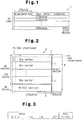
- Data to be recorded on a DVD-ROM is formatted as illustrated in Figure 1.
- a sector 1 includes an ID and reserve area of 12 bytes, user data of 2 Kbytes and an EDC (Error Detecting Code) of 4 bytes.
- Each sector 1 includes twelve rows of data which extend in the PI direction (row direction). The first row of data in each sector 1 consists of 172 bytes. Recorded in the first row are the 12-byte ID and reserve area and 160-byte user data. In the last row are recorded 168-byte user data and 4-byte EDC. Each of the intermediate rows has 172-bytes of user data.
- a data block 2 includes sixteen sectors 1, a PO-ECC section 3 and a PI-ECC section 4.
- the PO-ECC section 3 is an error correcting code for data in the PO direction (column direction) which exist over the individual sectors 1, and the PI-ECC section 4 is an error correcting code for data in each sector 1.
- the PI-ECC section 4 is affixed to generate a syndrome for error correction for each row in the PI direction in the data block 2 or for each PI interleave.
- the PO-ECC section 3 is affixed to generate a syndrome for error correction for each column in the PO direction in the data block 2 or for each PO interleave.
- the data block 2 is stored on the DVD-ROM in the encoding format as shown in Figure 5.
- the PO-ECC section 3 is segmented for the individual interleaves, with one interleave inserted between sectors 1.
- "One interleave" is a row or a column of data which includes user data and an error correcting code.
- the format can ensure high error detecting and correcting performance in an error correcting operation at the time of data reproduction.
- Figure 7 shows a syndrome operation unit which generates a syndrome in an error correcting operation.
- An EOR gate 5 receives data, read from a recording medium, byte by byte, and sends an output signal to a latch circuit 6.
- the latch circuit 6 receives the signal from the EOR gate 5 (Exclusive-OR) and sends a signal to a Galois constant multiplier 7.
- the Galois constant multiplier 7 performs an arithmetic operation on the signal received from the latch circuit 6.
- the Galois constant multiplier 7 sends an acquired Galois constant to the EOR gate 5.
- the syndrome operation unit every time data is sequentially input to the EOR gate 5, the latch circuit 6 outputs an error correcting syndrome Sy.
- step 1 When data in the PI direction from each sector 1 in the data block 2 is sequentially input byte by byte (step 1), PI syndromes are sequentially generated (step 2). At the same time, the input data in the PI direction is sequentially stored in a buffer memory for each interleave as shown in Figure 3 (step 3).
- step 4 When an error correcting syndrome Sy for one interleave in the PI direction is generated, the position and correction value for error data are computed interleave by interleave (step 4), and rewriting of the error data is carried out on the buffer memory (step 5). Such an operation is repeated for every PI interleave.
- the reason for rearranging the PO-ECC data in this manner is because the PO-ECC data is generated based on the data in each sector 1 which has continuously been read in the PO direction as shown in Figure 2. In other words, it is because arithmetic operations of syndromes have weights in the order of data input. Even when data, which has been weighed in the state shown in Figure 2, is input to the syndrome operation unit in the input order shown in Figure 6, the operation unit cannot generate accurate syndromes.
- step 8 When an error correcting syndrome for one interleave in the PO direction is generated, the position and correction value for error data are computed interleave by interleave (step 8), and rewriting of the error data is carried out on the buffer memory (step 9). The operation is repeated for every PO interleave. Through the operation, data read from the data block 2a is subjected to a high-precision error correcting operation both in the PI and PO directions.
- a recording medium like the aforementioned DVD-ROM is used as a data storage means which belongs to the peripheral devices of a computer, and an improvement on the operational speeds of computers demands faster error correction of data read from a recording medium.
- the above-described conventional error correction takes a relatively long time for data reading and writing with respect to a buffer memory and demands that time to be shortened.
- the operational speeds of computers increase, the time required for arithmetic operations for error correction is shortened while the time for data reading and writing with respect to a buffer memory is not shortened as much as desired.
- Reading and writing data to and from a buffer memory are executed in steps 3, 5 and 6 in the arithmetic operation on syndromes.
- step 5 data reading and writing with respect to the buffer memory are carried out for error correction of data, stored in the buffer memory, in the PI direction.
- step 6 data reading and writing with respect to the buffer memory are performed for rearranging data in the PO direction. To shorten the time required for rearranging the data in a different order, it is possible to previously store data in the buffer memory in a rearranged form (see Figure 2). However, even this case requires an operation for reading data from the buffer memory for error correction in the PO direction.
- the reason error correction takes so long is because error correction in the PI direction and error correction in the PO direction are not carried out in parallel.
- rearranging data in the PO direction is carried out, and then the error correction in the PO direction is performed.
- Even in the case where data is stored in the buffer memory in the state of the data block 2 shown in Figure 2 before error correction in the PI direction it is necessary to perform error correction in the PI direction after which data id read in the PO direction and is then subjected to error correction.
- the present invention provides a method of correcting an error in two-dimensional block data having row error correcting codes for individual rows of data and column error correcting codes for individual column of data, one column error correcting code being assigned to one column data group, individual column data groups and the individual column error correcting codes being alternately arranged, the method comprising the steps of: correcting errors in block data row by row using the row error correcting codes and row data; and correcting errors column by column in parallel to the row error correcting step, by using the column error correcting codes and column data.
- the present invention further provides a method of correcting an error in two-dimensional block data having row error correcting codes for individual rows of data and column error correcting codes for individual columns of data, one column error correcting code being assigned to a predetermined number of the column data, the column data and the individual column error correcting codes being alternately arranged, the row data and the column error correcting codes having a first weight according to a first order such that the individual column error correcting codes are arranged after all of the column data groups, the method comprising the steps of: correcting errors column by column using the row data and the row error correcting codes; receiving the column data; compensating the first weight for generating a second weight according to the received column data when the received column data is in a second order different from the first order; and correcting errors row by row based on the generated second weight, using the column data and the column error correcting codes.
- the present invention provides an error correcting apparatus for correcting an error in two-dimensional block data having row error correcting codes for individual rows of data and column error correcting codes for individual columns of data, one column error correcting code being assigned to one column data group, individual column data groups and the individual column error correcting codes being alternately arranged, the apparatus comprising: a control unit which corrects errors in block data row by row using the row error correcting codes and row data, and corrects errors column by column in parallel to the row error correcting, using the column error correcting codes and the column data.
- the present invention further provides an error correcting apparatus comprising: a control unit for correcting an error in two-dimensional block data having row error correcting codes for individual rows of data and column error correcting codes for individual column of data, one column error correcting code being assigned to one column data group, the column data group and the individual column error correcting codes being alternately arranged, the column data and the column error correcting codes having a first weight according to a first order such that the individual column error correcting codes are arranged after all column data groups; and a compensating device for compensating the first weight for generating a second weight according to the received column data when the received column data is in a second order different from the first order, wherein the control unit corrects errors column by column using the row data and the row error correcting codes, and corrects errors row by row based on the generated second weight using the column data and the column error correcting codes.
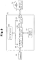
- an optical disk controller 21 is connected to a computer 22 via an interface, preferably ATAPI (AT Attachment Packet Interface).
- the optical disk controller 21 is also connected to an optical disk drive 23 via another interface.
- the optical disk drive 23 rotates a recording medium, i.e., a digital video disk (DVD) 24 at a predetermined velocity, and reads data recorded on the DVD 24 by means of an optical pickup (not shown). Then, the optical disk drive 23 sends the read data to the optical disk controller 21.
- a recording medium i.e., a digital video disk (DVD) 24 at a predetermined velocity
- DVD digital video disk
- the optical disk controller 21 comprises an optical disk control unit (hereinafter simply called control unit) 25, a microprocessor 26, a storage device, such as an external buffer memory 27, an interface circuit 28 and an input/output (I/O) driver 29.
- control unit optical disk control unit
- microprocessor a microprocessor
- storage device such as an external buffer memory 27, an interface circuit 28 and an input/output (I/O) driver 29.
- I/O input/output
- the control unit 25 carries out various processes, such as transfer of commands to the optical disk drive 23 and reception of status information therefrom, decoding of the read format from an optical disk and correction of errors in data therefrom, data transfer between the optical disk drive 23 and the buffer memory 27, and data transfer between the interface circuit 28 and the buffer memory 27.
- the control unit 25 receives data, read by the optical disk drive 23, via the I/O driver 29.
- the control unit 25 performs a process like error correction on the input data and stores the processed data in the buffer memory 27.
- the control unit 25 transfers data, stored in the buffer memory 27, to the computer 22 via the interface circuit 28.
- the control unit 25 is capable of generating error correcting syndromes in the PO direction without rearranging data even when PO interleaves are input in the order including PO-ECC data every 12 bytes, as shown in Figure 6, from a data block 2.
- the control unit 25 has a compensation input data generator 30 which comprises a data adjuster 31 and a Galois multiplier 32.
- the data adjuster 31 receives a data position signal from the optical disk drive 23.
- the data adjuster 31 computes a compensation Galois constant for compensating the input order of data based on data position signal, and sends the computed compensation Galois constant to the Galois multiplier 32.
- the Galois multiplier 32 receives the compensation Galois constant from the data adjuster 31 and data from the drive 23, and generates and outputs compensation input data a the compensated input order based on the computed compensation Galois constant.
- the data adjuster 31 computes the order affixed with a difference between the position of the input data and the original position of the data.
- the original position is the position of the data at the time of the conventional syndrome generation (see Figures 3 and 4), i.e., the position of the data which has been rearranged for the generation of syndromes.
- syndrome operation unit 50 (Fig. 11) computes correct syndromes even when receiving non-rearranged compensation input data, for the compensation input data already has an order weight which is included in the data corresponding to the input order for syndrome calculation.
- Sy(x) S n ⁇ X n + S n-1 ⁇ X n-1 + ... + S k ⁇ X k + ... +S k-1 ⁇ X k-1 + ... + S 0 ⁇ X 0
- Syi i-th coefficient of the syndrome Sy and ai denote the Galois constant
- Y ⁇ y 0 , y 1 , y 2 , ..., y k+1 , y k , ..., y n ⁇ and the input polynomial is expressed by the following equation (6).
- Y(X) y 0 ⁇ X n + y 1 ⁇ X n-1 + ... + y k+1 ⁇ X n-k + y k ⁇ X n-k-1 + ... + y n ⁇ X 0
- the compensation Galois constant compensates the input data for the Galois constant computation which is performed in the conventional syndrome calculation, based on the difference between the number of operations on the data position of the input data and those on the original data position (the difference in order).
- the number of operations of ai as an operational difference for the k-th data is decreased by one while the number of operations of ai as an operational difference for the (k+1)-th data is increased by one.
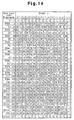
- the number of compensation computations for the input order of PO interleaves is determined according to a table as shown in Figure 13.
- the Galois constant ai is computed 195 times from the viewpoint of the input order, but the necessary number of operations is actually 15 times because the original input order is the 192nd. Based on the difference in the number of computations, therefore, the number of compensations is -180.
- the data adjuster 31 may be designed as shown in Figure 12 or Figures 16 to 18.
- the data adjuster 31 shown in Figure 12 has a correlation table 33 of the data positions of the input data and the original data positions of the input data.
- the data adjuster 31 extracts the original data position signal from the correlation table 33 based on the input data position signal.
- a difference calculator 34 receives the data position signal of the input data and the original data position signal, and computes a compensation Galois constant based on both signals.
- the second embodiment of the data adjuster 51 shown in Figure 16 has a calculator 35 for computing the original data position and a difference calculator 34 for computing a Galois constant.
- the calculator 35 computes the original data position signal based on the data position signal to be input.
- the difference calculator 34 receives both signals and computes a compensation Galois constant.
- the third embodiment of the data adjuster 52 shown in Figure 17 has a correlation table 36 of the data positions of the input data and compensation Galois constants corresponding to the data positions, and extracts an associated compensation Galois constant based on the input data position signal.
- the fourth embodiment of the data adjuster 53 shown in Figure 18 has a calculator 37 for computing the data position of input data and a compensation Galois constants corresponding to that data position, and calculates an associated compensation Galois constant based on the input data position signal.
- the correlation tables 33 and 36 and the calculators 35 and 57 may be properly combined as required.
- the correlation table or the calculator is properly selected based on the data position signal to compute a compensation Galois constant.
- Figure 14 shows a data table which holds compensation Galois constants with respect to the input order of PO interleaves.
- the individual constants are expressed by hexadecimal numbers.
- the syndrome operation unit 50 including a PI syndrome operation unit and a PO syndrome operation unit is equipped in the control unit 25 to generate syndromes in the PI direction and PO direction.
- the syndrome operation unit 50 comprises an EOR gate 38, a RAM 39, a Galois constant multiplier 40 and an initializer 41.
- the EOR gate 38 receives compensation input data from the Galois multiplier 32 and generates a syndrome Sy.
- the RAM 39 stores the generated syndrome Sy.
- the Galois constant multiplier 40 reads the syndrome Sy from the RAM 39 and sends a signal, obtained by computing the syndrome Sy, to the EOR gate 38 via the initializer 41.
- the initializer 41 receives the signal from the Galois constant multiplier 40 and an initialization signal "I", and initializes the syndrome from the Galois constant multiplier 40 based on the initialization signal I which is input, for example, when computation of the PO syndrome starts. When no initialization signal I is input, the initializer 41 sends the output signal of the Galois constant multiplier 40 directly to the EOR gate 38.
- the syndrome operation unit 50 can compute the syndrome of a PO interleave based on the data input sequentially in the PI direction.
- the syndrome acquired by the EOR gate 38 is temporarily stored in the RAM 39.
- the Galois constant multiplier 40 reads out the syndrome of the PO interleave from the RAM 39 and performs an operation thereon.
- the EOR gate 38 receives the computation result from the Galois constant multiplier 40 and generates a syndrome.
- the RAM 39 stores that syndrome. By repeating such an operation, the syndromes of the individual PO interleaves are generated based on the input compensation input data in the PI direction.
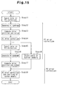
- the control unit 25 receives data in the PI direction from each sector 1 of the data block 2a, byte by byte (step 11), and sequentially generates PI syndromes for each single PI interleave (step 12).
- the control unit 25 When generating an error correcting syndrome of one interleave in the PI direction by means of the PI syndrome operation unit, the control unit 25 computes the position of error data in the interleave and a correction value for the error data (step 13), and performs an operation to rewrite the error data for one interleave stored in the control unit 25 (step 14).
- the control unit 25 repeats the above-described operation for every PI interleave and sequentially stores the corrected PI interleaves in the buffer memory 27 (step 18).
- the error correction in the PI direction consists of steps 1 to 14 and 18.
- the control unit 25 generates compensation input data from each corrected PI interleave through the operations of the data adjuster 31 and the Galois multiplier 32.
- the control unit 25 sends the compensation input data to the PO syndrome operation unit (step 15), and generates a PO syndrome in the PO syndrome operation unit (step 16).
- the control unit 25 sequentially generates syndromes of the individual PO interleaves based on the byte-by-byte inputs of the PO interleaves.
- a PI syndrome for the PI interleave to which that input data belongs is generated.
- one PO syndrome for the PO interleave to which the input data belongs is generated.
- One PI syndrome and one PO syndrome are generated in order in the mentioned manner for the input of one data in the PI direction.
- the control unit 25 computes the position of error data and a correction value for the data for each interleave (step 17), and performs an operation of rewriting the error data on the buffer memory 27 (step 18).
- the control unit 25 repeats such an operation for every PO interleave.
- the error correction in the PO direction steps 15 to 19.
- PI syndromes are generated without temporarily storing input data, read in the PI direction, in the buffer memory 27. After errors in data of PI interleaves are corrected, the individual PI interleaves are stored in the buffer memory 27. It is thus unnecessary to read data from the buffer memory 27 to correct an error in a PI interleave. This results in a reduced number of accesses to the buffer memory 27 and a shortened time for the generation of syndromes.
- a second embodiment of the present invention will now be described referring to Figure 19.
- the compensation input data generator and syndrome operation unit according to the second embodiment separately performs two operations on the 1-byte input data, one for the upper eight bytes and the other for the lower eight bytes according to the order.
- the data generator extracts a compensation Galois constant for the upper eight bytes from the compensation Galois constant correlation table 36 based on the data position signal of input data and the upper/lower identification (ID) signal, and computes corrected input data in the Galois multiplier 32.
- the upper syndrome operation unit computes a syndrome for the upper eight bytes based on data from the Galois multiplier 32 and the syndromes stored the RAM 39.
- the data generator likewise extracts a compensation Galois constant for the lower eight bytes from the table 36 and computes corrected input data in the Galois multiplier 32.
- the lower syndrome operation unit computes a syndrome for the lower eight bytes based on data from the Galois multiplier 32 and the syndromes stored in the RAM 39.
- the operational division by the operational order may be carried out every four bytes, every two bytes or every one byte, instead of the aforementioned units of eight bytes.
- Data error correcting apparatus like that of the second embodiment, performs a syndrome operation separately for upper and lower eight bytes, but by using a single syndrome operation unit, as shown in Figure 20.
- an identifying circuit 42 based on an upper/lower ID signal switches the generation of syndromes between the upper eight bytes and the lower eight bytes. This allows Galois constant multipliers 40c and 40d to operate in the same manner as the Galois constant multiplier in the second embodiment.
- the structure eliminates one EOR gate and further reduces the circuit scale.
Landscapes
- Physics & Mathematics (AREA)
- Mathematical Physics (AREA)
- Probability & Statistics with Applications (AREA)
- Engineering & Computer Science (AREA)
- Theoretical Computer Science (AREA)
- Algebra (AREA)
- General Physics & Mathematics (AREA)
- Pure & Applied Mathematics (AREA)
- Error Detection And Correction (AREA)
- Detection And Correction Of Errors (AREA)
Applications Claiming Priority (3)
| Application Number | Priority Date | Filing Date | Title |
|---|---|---|---|
| JP266582/97 | 1997-09-30 | ||
| JP26658297 | 1997-09-30 | ||
| JP9266582A JPH11112358A (ja) | 1997-09-30 | 1997-09-30 | データの誤り訂正方法及び誤り訂正装置 |
Publications (3)
| Publication Number | Publication Date |
|---|---|
| EP0905911A2 true EP0905911A2 (de) | 1999-03-31 |
| EP0905911A3 EP0905911A3 (de) | 2000-08-23 |
| EP0905911B1 EP0905911B1 (de) | 2014-03-05 |
Family
ID=17432817
Family Applications (1)
| Application Number | Title | Priority Date | Filing Date |
|---|---|---|---|
| EP98104856.4A Expired - Lifetime EP0905911B1 (de) | 1997-09-30 | 1998-03-18 | Verfahren und Vorrichtung zur Datenfehlerkorrektur |
Country Status (5)
| Country | Link |
|---|---|
| US (1) | US6167548A (de) |
| EP (1) | EP0905911B1 (de) |
| JP (1) | JPH11112358A (de) |
| KR (1) | KR100305973B1 (de) |
| TW (1) | TW418572B (de) |
Cited By (3)
| Publication number | Priority date | Publication date | Assignee | Title |
|---|---|---|---|---|
| EP1104114A3 (de) * | 1999-11-24 | 2004-02-11 | Sanyo Electric Co., Ltd. | Fehlerkorrektureinrichtung |
| US6772385B2 (en) | 2000-01-31 | 2004-08-03 | Sanyo Electric Co., Ltd. | Error-correcting device and decoder enabling fast error correction with reduced circuit scale |
| EP1801983A1 (de) * | 2005-12-20 | 2007-06-27 | Quantum Corporation | Fehlerkorrekturalgorithmus mit verschachtelter Paritätskontrolle und Reed-Solomon-Code |
Families Citing this family (11)
| Publication number | Priority date | Publication date | Assignee | Title |
|---|---|---|---|---|
| JP3530388B2 (ja) * | 1998-07-22 | 2004-05-24 | 三洋電機株式会社 | 符号誤り訂正装置 |
| JP2002074862A (ja) * | 2000-08-25 | 2002-03-15 | Toshiba Corp | データ処理方法及び装置及び記録媒体及び再生方法及び装置 |
| TW476932B (en) * | 2000-10-23 | 2002-02-21 | Acer Labs Inc | Decoding system for disk and the method thereof |
| TW479226B (en) * | 2000-12-15 | 2002-03-11 | Acer Labs Inc | Disc decoding system and method |
| TW522393B (en) * | 2001-02-02 | 2003-03-01 | Acer Labs Inc | Decoding system and method for disks |
| US6910174B2 (en) | 2001-06-01 | 2005-06-21 | Dphi Acquisitions, Inc. | Error correction code block format |
| US20030079161A1 (en) * | 2001-10-22 | 2003-04-24 | Verboom Johannes J. | Optimized data storage system and method for optical storage system |
| JP2005267719A (ja) * | 2004-03-17 | 2005-09-29 | Sanyo Electric Co Ltd | 符号化装置 |
| JP4247262B2 (ja) * | 2006-09-29 | 2009-04-02 | 株式会社東芝 | 集積回路装置 |
| US9189329B1 (en) | 2011-10-13 | 2015-11-17 | Marvell International Ltd. | Generating error correcting code (ECC) data using an ECC corresponding to an identified ECC protection level |
| US8959417B2 (en) * | 2011-11-23 | 2015-02-17 | Marvell World Trade Ltd. | Providing low-latency error correcting code capability for memory |
Citations (1)
| Publication number | Priority date | Publication date | Assignee | Title |
|---|---|---|---|---|
| US5631914A (en) | 1988-07-18 | 1997-05-20 | Canon Kabushiki Kaisha | Error correcting apparatus |
Family Cites Families (10)
| Publication number | Priority date | Publication date | Assignee | Title |
|---|---|---|---|---|
| JPS5961332A (ja) * | 1982-09-30 | 1984-04-07 | Nec Corp | 誤り訂正回路 |
| EP0156440B1 (de) * | 1984-03-24 | 1990-01-24 | Koninklijke Philips Electronics N.V. | Verfahren zur Informationsübertragung mit Fehlerkorrektur für Datenworte, ein Fehlerkorrektur-Dekodierverfahren für solche Datenworte, eine Anordnung zur Informationsübertragung zur Verwendung mit dem Verfahren, ein Gerät für Informationsdekodierung zur Verwendung mit dem Verfahren und eine Anordnung zur Verwendung mit solchem Gerät |
| JPS61154227A (ja) * | 1984-12-26 | 1986-07-12 | Mitsubishi Electric Corp | 2段符号化方法 |
| CA1264091A (en) * | 1986-01-10 | 1989-12-27 | Yoichiro Sako | Generator for error correcting code and decoder for the code |
| US4928280A (en) * | 1988-04-29 | 1990-05-22 | International Business Machines Corporation | Fast processor for multi-bit error correction codes |
| JPH0799503B2 (ja) * | 1990-09-12 | 1995-10-25 | パイオニア株式会社 | 符号化されたデータの誤り訂正方法 |
| US5392299A (en) * | 1992-01-15 | 1995-02-21 | E-Systems, Inc. | Triple orthogonally interleaed error correction system |
| JP3154607B2 (ja) * | 1993-12-28 | 2001-04-09 | 三菱電機株式会社 | 誤り訂正復号装置及び誤り訂正復号方法 |
| JP2970994B2 (ja) * | 1994-05-25 | 1999-11-02 | 三洋電機株式会社 | 誤り訂正復号回路 |
| US5627935A (en) * | 1994-11-11 | 1997-05-06 | Samsung Electronics Co., Ltd. | Error-correction-code coding & decoding procedures for the recording & reproduction of digital video data |
-
1997
- 1997-09-30 JP JP9266582A patent/JPH11112358A/ja active Pending
-
1998
- 1998-03-18 EP EP98104856.4A patent/EP0905911B1/de not_active Expired - Lifetime
- 1998-03-19 US US09/040,999 patent/US6167548A/en not_active Expired - Lifetime
- 1998-04-01 TW TW087104911A patent/TW418572B/zh not_active IP Right Cessation
- 1998-04-17 KR KR1019980013750A patent/KR100305973B1/ko not_active Expired - Fee Related
Patent Citations (1)
| Publication number | Priority date | Publication date | Assignee | Title |
|---|---|---|---|---|
| US5631914A (en) | 1988-07-18 | 1997-05-20 | Canon Kabushiki Kaisha | Error correcting apparatus |
Cited By (6)
| Publication number | Priority date | Publication date | Assignee | Title |
|---|---|---|---|---|
| EP1104114A3 (de) * | 1999-11-24 | 2004-02-11 | Sanyo Electric Co., Ltd. | Fehlerkorrektureinrichtung |
| US6802040B1 (en) | 1999-11-24 | 2004-10-05 | Sanyo Electric Co., Ltd. | Error correction device |
| US6772385B2 (en) | 2000-01-31 | 2004-08-03 | Sanyo Electric Co., Ltd. | Error-correcting device and decoder enabling fast error correction with reduced circuit scale |
| US7181483B2 (en) | 2000-01-31 | 2007-02-20 | Sanyo Electric Co., Ltd. | Error-correcting device and decoder enabling fast error correction with reduced circuit scale |
| EP1801983A1 (de) * | 2005-12-20 | 2007-06-27 | Quantum Corporation | Fehlerkorrekturalgorithmus mit verschachtelter Paritätskontrolle und Reed-Solomon-Code |
| US7694208B2 (en) | 2005-12-20 | 2010-04-06 | Quantum Corporation | Error correction algorithm using interleaved parity check and Reed-Solomon code |
Also Published As
| Publication number | Publication date |
|---|---|
| KR100305973B1 (ko) | 2001-10-19 |
| TW418572B (en) | 2001-01-11 |
| EP0905911A3 (de) | 2000-08-23 |
| JPH11112358A (ja) | 1999-04-23 |
| EP0905911B1 (de) | 2014-03-05 |
| US6167548A (en) | 2000-12-26 |
| KR19990029163A (ko) | 1999-04-26 |
Similar Documents
| Publication | Publication Date | Title |
|---|---|---|
| US4881232A (en) | Method and apparatus for error correction | |
| KR100517482B1 (ko) | 곱셈 코드에 대한 동시 행/열 신드롬 발생기 | |
| US6158038A (en) | Method and apparatus for correcting data errors | |
| US5027357A (en) | ECC/CRC error detection and correction system | |
| US6357030B1 (en) | ECC block format for storage device | |
| US6167548A (en) | Data error correcting method and apparatus | |
| US7600177B2 (en) | Delta syndrome based iterative Reed-Solomon product code decoder | |
| US6041431A (en) | Method and apparatus for performing error correction code operations | |
| US6018626A (en) | Error correction method and apparatus for disk drive emulator | |
| US7962833B2 (en) | Unified memory architecture for recording applications | |
| US6725416B2 (en) | Forward error correction apparatus and methods | |
| US6772385B2 (en) | Error-correcting device and decoder enabling fast error correction with reduced circuit scale | |
| US8201061B2 (en) | Decoding error correction codes using a modular single recursion implementation | |
| US4593394A (en) | Method capable of simultaneously decoding two reproduced sequences | |
| US5956757A (en) | Method and apparatus for generating addresses | |
| JP3281387B2 (ja) | Crc/edcチェッカシステム | |
| KR100738170B1 (ko) | 오류 정정 장치 | |
| US6128760A (en) | Method and apparatus for calculating a CRC remainder | |
| JP3306413B2 (ja) | 誤り訂正装置および誤り訂正方法 | |
| KR20000023004A (ko) | 디스크 재생 장치에 적용되는 에러 검출 회로 | |
| JPS638648B2 (de) | ||
| JPH04365139A (ja) | 誤り訂正処理用シンドローム演算回路 | |
| JP3773740B2 (ja) | 復号装置 | |
| KR100215807B1 (ko) | 디지탈 신호의 에러 정정 장치 및 방법 | |
| JP3135552B2 (ja) | リードソロモン符号の誤り検出及び訂正装置 |
Legal Events
| Date | Code | Title | Description |
|---|---|---|---|
| PUAI | Public reference made under article 153(3) epc to a published international application that has entered the european phase |
Free format text: ORIGINAL CODE: 0009012 |
|
| AK | Designated contracting states |
Kind code of ref document: A2 Designated state(s): DE FR |
|
| AX | Request for extension of the european patent |
Free format text: AL;LT;LV;MK;RO;SI |
|
| PUAL | Search report despatched |
Free format text: ORIGINAL CODE: 0009013 |
|
| AK | Designated contracting states |
Kind code of ref document: A3 Designated state(s): AT BE CH DE DK ES FI FR GB GR IE IT LI LU MC NL PT SE |
|
| AX | Request for extension of the european patent |
Free format text: AL;LT;LV;MK;RO;SI |
|
| RIC1 | Information provided on ipc code assigned before grant |
Free format text: 7H 03M 13/00 A, 7G 11B 20/18 B, 7H 03M 13/27 B |
|
| AKX | Designation fees paid |
Free format text: DE FR |
|
| 17P | Request for examination filed |
Effective date: 20010213 |
|
| R17P | Request for examination filed (corrected) |
Effective date: 20010213 |
|
| 17Q | First examination report despatched |
Effective date: 20050804 |
|
| 17Q | First examination report despatched |
Effective date: 20050804 |
|
| RAP1 | Party data changed (applicant data changed or rights of an application transferred) |
Owner name: FUJITSU MICROELECTRONICS LIMITED |
|
| RAP1 | Party data changed (applicant data changed or rights of an application transferred) |
Owner name: FUJITSU SEMICONDUCTOR LIMITED |
|
| REG | Reference to a national code |
Ref country code: DE Ref legal event code: R079 Ref document number: 69843211 Country of ref document: DE Free format text: PREVIOUS MAIN CLASS: H03M0013000000 Ipc: H03M0013150000 |
|
| RIC1 | Information provided on ipc code assigned before grant |
Ipc: H03M 13/15 20060101AFI20130711BHEP Ipc: G11B 20/18 20060101ALI20130711BHEP |
|
| GRAP | Despatch of communication of intention to grant a patent |
Free format text: ORIGINAL CODE: EPIDOSNIGR1 |
|
| INTG | Intention to grant announced |
Effective date: 20130918 |
|
| GRAS | Grant fee paid |
Free format text: ORIGINAL CODE: EPIDOSNIGR3 |
|
| GRAA | (expected) grant |
Free format text: ORIGINAL CODE: 0009210 |
|
| AK | Designated contracting states |
Kind code of ref document: B1 Designated state(s): DE FR |
|
| REG | Reference to a national code |
Ref country code: DE Ref legal event code: R096 Ref document number: 69843211 Country of ref document: DE Effective date: 20140410 |
|
| REG | Reference to a national code |
Ref country code: DE Ref legal event code: R097 Ref document number: 69843211 Country of ref document: DE |
|
| PLBE | No opposition filed within time limit |
Free format text: ORIGINAL CODE: 0009261 |
|
| STAA | Information on the status of an ep patent application or granted ep patent |
Free format text: STATUS: NO OPPOSITION FILED WITHIN TIME LIMIT |
|
| 26N | No opposition filed |
Effective date: 20141208 |
|
| REG | Reference to a national code |
Ref country code: DE Ref legal event code: R097 Ref document number: 69843211 Country of ref document: DE Effective date: 20141208 |
|
| REG | Reference to a national code |
Ref country code: FR Ref legal event code: ST Effective date: 20150213 |
|
| REG | Reference to a national code |
Ref country code: DE Ref legal event code: R082 Ref document number: 69843211 Country of ref document: DE Representative=s name: REICHERT & LINDNER PARTNERSCHAFT PATENTANWAELT, DE |
|
| REG | Reference to a national code |
Ref country code: DE Ref legal event code: R082 Ref document number: 69843211 Country of ref document: DE Representative=s name: REICHERT & LINDNER PARTNERSCHAFT PATENTANWAELT, DE Effective date: 20150331 Ref country code: DE Ref legal event code: R081 Ref document number: 69843211 Country of ref document: DE Owner name: SOCIONEXT INC., YOKOHAMA-SHI, JP Free format text: FORMER OWNER: FUJITSU LIMITED, KAWASAKI-SHI, KANAGAWA, JP Effective date: 20140305 Ref country code: DE Ref legal event code: R081 Ref document number: 69843211 Country of ref document: DE Owner name: SOCIONEXT INC., YOKOHAMA-SHI, JP Free format text: FORMER OWNER: FUJITSU SEMICONDUCTOR LTD., YOKOHAMA-SHI, KANAGAWA, JP Effective date: 20150331 Ref country code: DE Ref legal event code: R081 Ref document number: 69843211 Country of ref document: DE Owner name: SOCIONEXT INC., YOKOHAMA-SHI, JP Free format text: FORMER OWNER: FUJITSU LTD., KAWASAKI-SHI, KANAGAWA-KEN, JP Effective date: 20140305 |
|
| PG25 | Lapsed in a contracting state [announced via postgrant information from national office to epo] |
Ref country code: FR Free format text: LAPSE BECAUSE OF NON-PAYMENT OF DUE FEES Effective date: 20140505 |
|
| PGFP | Annual fee paid to national office [announced via postgrant information from national office to epo] |
Ref country code: DE Payment date: 20160330 Year of fee payment: 19 |
|
| REG | Reference to a national code |
Ref country code: DE Ref legal event code: R119 Ref document number: 69843211 Country of ref document: DE |
|
| PG25 | Lapsed in a contracting state [announced via postgrant information from national office to epo] |
Ref country code: DE Free format text: LAPSE BECAUSE OF NON-PAYMENT OF DUE FEES Effective date: 20171003 |