EP0907206A1 - Substratdurchkontakt und Herstellungsverfahren dafür - Google Patents
Substratdurchkontakt und Herstellungsverfahren dafür Download PDFInfo
- Publication number
- EP0907206A1 EP0907206A1 EP98118519A EP98118519A EP0907206A1 EP 0907206 A1 EP0907206 A1 EP 0907206A1 EP 98118519 A EP98118519 A EP 98118519A EP 98118519 A EP98118519 A EP 98118519A EP 0907206 A1 EP0907206 A1 EP 0907206A1
- Authority
- EP
- European Patent Office
- Prior art keywords
- substrate
- via hole
- layer
- forming
- over
- Prior art date
- Legal status (The legal status is an assumption and is not a legal conclusion. Google has not performed a legal analysis and makes no representation as to the accuracy of the status listed.)
- Granted
Links
Images





Classifications
-
- H—ELECTRICITY
- H10—SEMICONDUCTOR DEVICES; ELECTRIC SOLID-STATE DEVICES NOT OTHERWISE PROVIDED FOR
- H10D—INORGANIC ELECTRIC SEMICONDUCTOR DEVICES
- H10D84/00—Integrated devices formed in or on semiconductor substrates that comprise only semiconducting layers, e.g. on Si wafers or on GaAs-on-Si wafers
- H10D84/01—Manufacture or treatment
- H10D84/02—Manufacture or treatment characterised by using material-based technologies
- H10D84/05—Manufacture or treatment characterised by using material-based technologies using Group III-V technology
-
- H—ELECTRICITY
- H10—SEMICONDUCTOR DEVICES; ELECTRIC SOLID-STATE DEVICES NOT OTHERWISE PROVIDED FOR
- H10W—GENERIC PACKAGES, INTERCONNECTIONS, CONNECTORS OR OTHER CONSTRUCTIONAL DETAILS OF DEVICES COVERED BY CLASS H10
- H10W20/00—Interconnections in chips, wafers or substrates
- H10W20/01—Manufacture or treatment
- H10W20/021—Manufacture or treatment of interconnections within wafers or substrates
- H10W20/023—Manufacture or treatment of interconnections within wafers or substrates the interconnections being through-semiconductor vias
-
- H—ELECTRICITY
- H10—SEMICONDUCTOR DEVICES; ELECTRIC SOLID-STATE DEVICES NOT OTHERWISE PROVIDED FOR
- H10W—GENERIC PACKAGES, INTERCONNECTIONS, CONNECTORS OR OTHER CONSTRUCTIONAL DETAILS OF DEVICES COVERED BY CLASS H10
- H10W20/00—Interconnections in chips, wafers or substrates
- H10W20/01—Manufacture or treatment
- H10W20/021—Manufacture or treatment of interconnections within wafers or substrates
- H10W20/023—Manufacture or treatment of interconnections within wafers or substrates the interconnections being through-semiconductor vias
- H10W20/0238—Manufacture or treatment of interconnections within wafers or substrates the interconnections being through-semiconductor vias comprising etching via holes through pads or through electrodes
-
- H—ELECTRICITY
- H10—SEMICONDUCTOR DEVICES; ELECTRIC SOLID-STATE DEVICES NOT OTHERWISE PROVIDED FOR
- H10W—GENERIC PACKAGES, INTERCONNECTIONS, CONNECTORS OR OTHER CONSTRUCTIONAL DETAILS OF DEVICES COVERED BY CLASS H10
- H10W20/00—Interconnections in chips, wafers or substrates
- H10W20/01—Manufacture or treatment
- H10W20/021—Manufacture or treatment of interconnections within wafers or substrates
- H10W20/023—Manufacture or treatment of interconnections within wafers or substrates the interconnections being through-semiconductor vias
- H10W20/0245—Manufacture or treatment of interconnections within wafers or substrates the interconnections being through-semiconductor vias comprising use of blind vias during the manufacture
-
- H—ELECTRICITY
- H10—SEMICONDUCTOR DEVICES; ELECTRIC SOLID-STATE DEVICES NOT OTHERWISE PROVIDED FOR
- H10W—GENERIC PACKAGES, INTERCONNECTIONS, CONNECTORS OR OTHER CONSTRUCTIONAL DETAILS OF DEVICES COVERED BY CLASS H10
- H10W20/00—Interconnections in chips, wafers or substrates
- H10W20/20—Interconnections within wafers or substrates, e.g. through-silicon vias [TSV]
-
- H—ELECTRICITY
- H10—SEMICONDUCTOR DEVICES; ELECTRIC SOLID-STATE DEVICES NOT OTHERWISE PROVIDED FOR
- H10W—GENERIC PACKAGES, INTERCONNECTIONS, CONNECTORS OR OTHER CONSTRUCTIONAL DETAILS OF DEVICES COVERED BY CLASS H10
- H10W20/00—Interconnections in chips, wafers or substrates
- H10W20/20—Interconnections within wafers or substrates, e.g. through-silicon vias [TSV]
- H10W20/211—Through-semiconductor vias, e.g. TSVs
- H10W20/212—Top-view shapes or dispositions, e.g. top-view layouts of the vias
- H10W20/2125—Top-view shapes
Definitions
- the present invention relates to an electronic device used for a mobile communication unit or the like in the field of information/telecommunication technology and a method for fabricating the same.
- GaAs gallium arsenide
- a large number of GaAs FETs are formed on a semi-insulating substrate made of GaAs. Then, during mounting, the substrate is divided by dicing into respective chips. Each of the divided chips is mounted on a lead frame. Thereafter, the electrodes of each GaAs FET are electrically connected to the lead frame via an Au wire.
- a method for electrically connecting the electrodes of an FET formed on a GaAs substrate to a lead frame through a conductor layer filled in a via hole formed in the GaAs substrate is suggested in Japanese Laid-Open Publication No. 6-5880, for example.
- the distance between the electrodes of the FET and the lead frame to be connected thereto can be shortened compared with connecting the electrodes to the lead frame via an Au wire.
- the parasitic inductance can be considerably reduced and the decrease in gain of the FET can be prevented.
- an FET including an active layer 12 , a source electrode 13 , a drain electrode 14 and a gate electrode 15 , is formed on the principal surface of a substrate 11 made of GaAs and having a thickness of 600 ⁇ m. Then, as shown in Figure 12(b) , the back surface of the substrate 11 is polished to have the thickness thereof reduced to several tens to one hundred and several tens ⁇ m.
- an etching mask 16 having an opening 16a at a site corresponding to the source electrode 13 is formed on the back surface of the substrate 11 , and the substrate 11 is etched using this mask 16 , thereby forming a via hole 17 in the substrate 11 so as to reach the back surface of the source electrode 13 .
- the etching mask 16 is removed, and a plating undercoat layer 18 is formed over the entire back surface of the substrate 11 as well as the wall and bottom surfaces of the via hole 17 .
- a metal electrode 19 is formed over the plating undercoat layer 18 by electroplating technique such that the via hole 17 is filled in with the metal electrode 19 .
- an electronic device which includes the substrate 11 with a reduced thickness and in which the source electrode 13 is electrically connected to the metal electrode 19 , can be obtained. It is noted that the plating undercoat layer 18 improves the adhesion of the metal electrode 19 to the substrate 11 .
- the substrate 11 is likely to crack.
- the thinned substrate 11 In order to form the via hole 17 , the thinned substrate 11 must be transported to an apparatus for forming the etching mask 16 and then to an apparatus for etching the substrate 11 . That is to say, since the substrate 11 , which has the mechanical strength thereof decreased because of the reduction in thickness thereof, should be transported to these apparatuses, the substrate 11 is more likely to crack during the transportation. Thus, in accordance with the conventional method for fabricating an electronic device, the production yield adversely decreases.
- the etching mask 16 having the opening 16a at the site corresponding to the source electrode 13 should be formed over the back surface of the substrate 11 . Accordingly, during this process step, the position of the source electrode 13 formed on the principal surface of the substrate 11 should be aligned with the position of the opening 16a of the etching mask 16 formed on the back surface of the substrate 11 .
- a special aligner in order to align the position of the source electrode 13 on the principal surface of the substrate 11 with the position of the opening 16a of the etching mask 16 on the back surface thereof, a special aligner must be used. In addition, the process step required is adversely complicated and difficult.
- the objects of the present invention are to prevent a decrease in production yield because of cracking of a substrate during the transportation step for forming a via hole in the substrate, and to eliminate a complicated alignment step conventionally required for forming a via hole in the substrate.
- a first method for fabricating an electronic device includes the steps of: a) forming a via hole in the principal surface of a substrate, the via hole having a bottom; b) forming a conductor layer at least over a sidewall of the via hole; and c) thinning the substrate by removing a portion of the substrate such that the conductor layer is exposed, the portion of the substrate being opposite to another portion of the substrate in which the via hole is formed.
- a via hole having a bottom is formed in the principal surface of a substrate, a conductor layer is formed at least over a sidewall of the via hole, and then the substrate is thinned by removing a portion of the substrate opposite to another portion of the substrate in which the via hole is formed such that the conductor layer is exposed.
- the steps of forming the via hole in the substrate and forming the conductor layer in the via hole can be performed on a substrate that has not been thinned yet and thus still retains a sufficient mechanical strength. Accordingly, the step of transporting a thinned substrate to an apparatus for forming a via hole or to an apparatus for forming a conductor layer need not be performed. As a result, it is possible to prevent the substrate from cracking during the transportation of the substrate to these apparatuses and the production yield of the electronic device can be increased as compared with a conventional method.
- the method preferably further includes, prior to the step a), the step of d) forming an electrode layer on the principal surface of the substrate, the electrode layer having a through hole over a region where the via hole is to be formed.
- the step a) preferably includes the steps of: forming an etching mask over the principal surface of the substrate as well as over the electrode layer, the etching mask having an opening over the region where the via hole is to be formed; and etching the substrate using the etching mask to form the via hole.
- an electrode layer having a via hole is formed over a region where the via hole is to be formed, the via hole is formed by etching the substrate using an etching mask having an opening over the region where the via hole is to be formed, and then a conductor layer is formed at least over a sidewall of the via hole.
- an interconnection layer connecting the electrode layer to the conductor layer is no longer necessary. As a result, the number of required process steps can be reduced.
- the step b) preferably includes the step of filling in the via hole with the conductor layer.
- the electrode layer formed on the principal surface of the substrate can be connected to the conductor layer with more certainty.
- the step b) preferably includes the step of forming the conductor layer by electron beam evaporation technique such that the conductor layer includes a sidewall portion and a bottom portion and has a recess at the center thereof.
- the conductor layer can be formed in a short period of time.
- the step c) preferably includes the step of removing the portion of the substrate opposite to the portion of the substrate in which the via hole is formed such that the bottom portion of the conductor layer is left.
- the step b) preferably includes the steps of forming a plating undercoat layer over the sidewall of the via hole and filling in the inside of the plating undercoat layer with the conductor layer.
- a metal which is usually hard to be directly plated over the substrate, can be used as a material for the conductor layer. Accordingly, it is possible to broaden the range from which a material for forming the conductor layer is selected.
- the substrate is preferably a semi-insulating substrate made of a Group III-V compound such as gallium arsenide and indium phosphide.
- a semi-insulating substrate made of a Group III-V compound easily cracks by nature.
- the substrate can be thinned without making the substrate crack.
- a second method for fabricating an electronic device includes the steps of: a) forming an electrode layer on the principal surface of a substrate; b) forming a first plating undercoat layer over the entire principal surface of the substrate; c) depositing an insulator film over the first plating undercoat layer, the insulator film having an opening over a region where a via hole is to be formed, a surrounding region thereof and at least part of the electrode layer; d) forming an etching mask over the first plating undercoat layer and the insulator film, the etching mask having an opening over the region where the via hole is to be formed; e) forming the via hole having a bottom through the first plating undercoat layer and in the substrate by etching the substrate using the etching mask; f) forming a second plating undercoat layer over the etching mask as well as over the inside of the via hole; g) leaving the second plating undercoat layer inside the via hole by lifting off the second plating undercoat layer and the etching
- the steps of forming the via hole in the substrate and forming the conductor layer in the via hole can be performed on a substrate that has not been thinned yet and thus still retains a sufficient mechanical strength, as in the first method for fabricating an electronic device. Accordingly, the step of transporting a thinned substrate to an apparatus for forming a via hole or to an apparatus for forming a conductor layer need not be performed. As a result, it is possible to prevent the substrate from cracking during the transportation of the substrate to these apparatuses and the production yield of the electronic device can be increased as compared with a conventional method.
- metal plating is performed by using, as a mask, an insulator film having an opening over a region where a via hole is formed, a surrounding region thereof and at least part of the electrode layer, thereby forming a metal layer to cover the opening of the insulator film as well as the inside of the via hole.
- the metal film connected to the electrode layer formed on the principal surface of the substrate reaches the region surrounding the region where the via hole is formed, the electrical characteristics of the electronic device can be tested by connecting a tester electrode to the metal film reaching the surrounding region. Accordingly, the electrical characteristics of the electronic device already including the via hole can be performed while the substrate has not been thinned yet and thus still retains a sufficient mechanical strength.
- the substrate of an electronic device having defective electrical characteristics is not thinned in vain.
- the step h) preferably includes the step of forming the metal layer in such a shape as including a sidewall portion and a bottom portion and has a recess at the center thereof.
- the step i) preferably includes the step of removing the portion of the substrate opposite to the portion of the substrate in which the via hole is formed such that the bottom portion of the metal layer is left.
- the contact area between an electrode layer formed on the back surface opposite to the principal surface of the substrate and the conductor layer becomes large.
- contact resistance between the electrode layer on the back surface and the conductor layer can be reduced.
- a first electronic device includes: an electrode layer formed on a substrate; a via hole formed in the vicinity of the electrode layer in the substrate; and a conductor layer formed at least over a sidewall of the via hole and electrically connected to the electrode layer.
- the via hole has a cross-sectional shape, at least part of which has an interior angle equal to or larger than 180 degrees.
- At least part of the cross section of the via hole has an interior angle equal to or larger than 180 degrees.
- the contact area between the conductor layer formed at least over the sidewall of the via hole and the substrate is larger.
- the adhesion between the conductor layer and the substrate increases and the conductor layer is less likely to peel off the substrate.
- a second electronic device includes: an electrode layer formed on a substrate; a via hole formed in the vicinity of the electrode layer in the substrate; and a conductor layer formed at least over a sidewall of the via hole and electrically connected to the electrode layer.
- the conductor layer has an area with which a probe needle is able to make electrical contact.
- the conductor layer has an area with which a probe needle is able to make electrical contact.
- the electrical characteristics of the electronic device can be tested by connecting a probe needle to an exposed part of the conductor layer on the back surface of the substrate. Since the electrical characteristics of the electronic device can be tested before a metal electrode is formed on the back surface of the substrate, the metal electrode is not formed in vain for an electronic device having defective electrical characteristics.
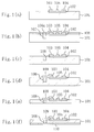
- arsenic ions are selectively implanted into the principal surface portion of a substrate 101 made of GaAs and having a thickness of 150 ⁇ m by using a resist mask. Then, heat treatment is conducted to activate the impurity, thereby forming an active layer 102 having a thickness of 0.2 ⁇ m. Thereafter, a first resist mask, having openings over respective regions where source/drain electrodes are to be formed, is formed over the active layer 102 .
- an alloy film of gold and germanium and a gold film are sequentially deposited over the first resist mask and the first resist mask is lifted off, thereby forming source/drain electrodes 103 and 104 to be in ohmic contact with the active layer 102 .
- a second resist mask having an opening over a region where a gate electrode is to be formed, is formed over the active layer 102 .
- a titanium film having a thickness of 0.05 ⁇ m and an aluminum film having a thickness of 0.5 ⁇ m are sequentially deposited over the second resist mask and the second resist mask is lifted off, thereby forming a gate electrode 105 to be in Schottky contact with the active layer 102 .
- an FET including the active layer 102 , the source electrode 103 , the drain electrode 104 and the gate electrode 105 is obtained. It is noted that the gap between the source electrode 103 and the gate electrode 105 and the gap between the drain electrode 104 and the gate electrode 105 are both 1 ⁇ m.
- an etching mask 106 having an opening 106a over a region where a via hole is to be formed and having a thickness of 20 ⁇ m is formed over the principal surface of the substrate 101 .
- the substrate 101 is etched using the etching mask 106 , thereby forming a via hole 107 having a depth of 200 ⁇ m and a bottom in the substrate 101 .
- One side of the via hole 107 is 20 ⁇ m long.
- a conductor layer 108 made of platinum, for example, is filled in the via hole 107 in accordance with electroless plating technique or the like and then the etching mask 106 is removed.
- the source electrode 103 is connected to the conductor layer 108 in accordance with known lithography technique and an interconnection layer 109 made of gold and having a thickness of 0.5 ⁇ m is formed.
- a metal electrode 110 made of gold, is deposited over the entire back surface of the substrate 101 .
- the interconnection layer 109 connected to the source electrode 103 is electrically connected to the metal electrode 110 by way of the conductor layer 108 filled in the via hole 107 .
- the steps of forming the via hole 107 in the substrate 101 and filling in the via hole 107 with the conductor layer 108 can be performed on the substrate 101 that has not been thinned yet and thus still retains a sufficient mechanical strength. Accordingly, it is possible to prevent the substrate from cracking while the sub-strate 101 thinned is transported to perform the steps of forming the via hole and the conductor layer. As a result, the production yield of the electronic device can be increased as compared with a conventional method.
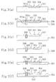
- arsenic ions are selectively implanted into the principal surface portion of a substrate 201 made of GaAs and having a thickness of 150 ⁇ m. Then, heat treatment is conducted to activate the impurity, thereby forming an active layer 202 having a thickness of 0.2 ⁇ m. Thereafter, source/drain electrodes 203 and 204 in ohmic contact with the active layer 202 and a gate electrode 205 in Schottky contact with the active layer 202 are formed in the same way as in the first embodiment. In this manner, an FET including the active layer 202 , the source electrode 203 , the drain electrode 204 and the gate electrode 205 is obtained.
- the source electrode 203 is formed to extend in the direction away from the gate electrode 205 and has an opening 203a over a region where a via hole is to be formed, unlike the source electrode 103 of the first embodiment.
- One side of the opening 203a is 20 ⁇ m long.
- an etching mask 206 having an opening 206a , which communicates with the opening 203a of the source electrode 203 , and having a thickness of 20 ⁇ m is formed over the principal surface of the substrate 201 .
- the substrate 201 is etched using the etching mask 206 , thereby forming a via hole 207 having a depth of 200 ⁇ m and a bottom and communicating with the opening 203a of the source electrode 203 in the substrate 201 .
- One side of the via hole 207 is 20 ⁇ m long.
- a conductor layer 208 made of platinum, for example, is filled in the via hole 207 by electroless plating technique, and the etching mask 206 is removed.
- the back surface portion of the substrate 201 (opposite to the portion where the via hole 207 is formed) is removed such that the conductor layer 208 is exposed, thereby thinning the substrate 201 .
- a metal electrode 209 made of gold, is deposited over the entire back surface of the substrate 201 .
- the source electrode 203 is electrically connected to the metal electrode 209 by way of the conductor layer 208 filled in the via hole 207 .
- the steps of forming the via hole 207 in the substrate 201 and filling in the via hole 207 with the conductor layer 208 can be performed on the substrate 201 that has not been thinned yet and thus still retains a sufficient mechanical strength. Accordingly, it is possible to prevent the substrate from cracking while the substrate 201 thinned is transported to perform the steps of forming the via hole and the conductor layer. As a result, the production yield of the electronic device can be increased as compared with a conventional method.
- the source electrode 203 can be connected to the metal electrode 209 by filling in the opening 203a of the source electrode 203 and the via hole 207 with the conductor layer 208 .
- the interconnection layer 109 which is required in the first embodiment for connecting the source electrode 103 to the conductor layer 108 , is not necessary. Accordingly, the process can be simplified as compared with the first embodiment.
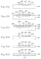
- arsenic ions are selectively implanted into the principal surface portion of a substrate 301 made of GaAs and having a thickness of 150 ⁇ m. Then, heat treatment is conducted to activate the impurity, thereby forming an active layer 302 having a thickness of 0.2 ⁇ m. Thereafter, source/drain electrodes 303 and 304 in ohmic contact with the active layer 302 and a gate electrode 305 in Schottky contact with the active layer 302 are formed in the same way as in the first embodiment. In this manner, an FET including the active layer 302 , the source electrode 303 , the drain electrode 304 and the gate electrode 305 is obtained.
- the source electrode 303 is formed to extend in the direction away from the gate electrode 305 and has an opening 303a over a region where a via hole is to be formed, as in the second embodiment.
- an etching mask 306 having an opening 306a , which communicates with the opening 303a of the source electrode 303 , and having a thickness of 20 ⁇ m is formed over the principal surface of the substrate 301 .
- the substrate 301 is etched using the etching mask 306 , thereby forming a via hole 307 having a depth of 200 ⁇ m and a bottom and communicating with the opening 303a of the source electrode 303 in the substrate 301 .
- One side of the via hole 307 is 20 ⁇ m long.
- a conductor layer 309 made of platinum, for example, is filled in the plating undercoat layer 308 by electroless plating technique.
- the back surface portion of the substrate 301 (opposite to the portion where the via hole 307 is formed) is removed such that the conductor layer 309 is exposed, thereby thinning the substrate 301 .
- a metal electrode 310 made of gold, is deposited over the entire back surface of the substrate 301 .
- the source electrode 303 is electrically connected to the metal electrode 310 by way of the plating undercoat layer 308 and the conductor layer 309 formed in the via hole 307 .
- the steps of forming the via hole 307 in the substrate 301 and filling in the via hole 307 with the conductor layer 309 can be performed on the substrate 301 that has not been thinned yet and thus still retains a sufficient mechanical strength. Accordingly, it is possible to prevent the substrate from cracking while the substrate 301 thinned is transported to perform the steps of forming the via hole and the conductor layer. As a result, the production yield of the electronic device can be increased as compared with a conventional method.
- the source electrode 303 can be connected to the metal electrode 310 by filling in the opening 303a of the source electrode 303 and the via hole 307 with the conductor layer 309 .
- the interconnection layer 109 which is required in the first embodiment for connecting the source electrode 103 to the conductor layer 108 , is not necessary. Accordingly, the process can be simplified as compared with the first embodiment.
- the plating undercoat metal layer 308 is formed over the sidewalls and bottom of the via hole 307 and then the plating undercoat layer 308 is filled in with the conductor layer 309 by electroless plating technique.
- the conductor layer may be made of a metal (e.g., gold) that is usually hard to be directly plated over the substrate 301 .
- the conductor layer 309 is formed by electroless plating technique.
- the conductor layer 309 may be formed by any other plating technique or evaporation technique.
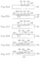
- arsenic ions are selectively implanted into the principal surface portion of a substrate 401 made of GaAs and having a thickness of 150 ⁇ m. Then, heat treatment is conducted to activate the impurity, thereby forming an active layer 402 having a thickness of 0.2 ⁇ m. Thereafter, source/drain electrodes 403 and 404 in ohmic contact with the active layer 402 and a gate electrode 405 in Schottky contact with the active layer 402 are formed in the same way as in the first embodiment. In this manner, an FET including the active layer 402 , the source electrode 403 , the drain electrode 404 and the gate electrode 405 is obtained.
- the source electrode 403 is formed to extend in the direction away from the gate electrode 405 and has an opening 403a over a region where a via hole is to be formed, unlike the source electrode 103 of the first embodiment.
- an etching mask 406 having an opening 406a , which communicates with the opening 403a of the source electrode 403 , and having a thickness of 20 ⁇ m is formed over the principal surface of the substrate 401 .
- the substrate 401 is etched using the etching mask 406 , thereby forming a via hole 407 having a depth of 200 ⁇ m and a bottom and communicating with the opening 403a of the source electrode 403 in the substrate 401 .
- One side of the via hole 407 is 20 ⁇ m long.
- a suspension in which metal particles of platinum are turned into sol in the presence of an organic solvent, is applied over the entire surface of the substrate 401 as well as the inside of the via hole 407 . Thereafter, the suspension is dried and the organ-ic solvent is evaporated, thereby forming a metal particle layer 408 inside the via hole 407 and over the etching mask 406 .
- the etching mask 406 and a part of the metal particle layer 408 existing over the etching mask 406 are lifted off and removed. And the remaining part of the metal particle layer 408 is sintered by heating the substrate 401 , thereby forming a conductor layer 409 out of the metal particle layer 408 inside the via hole 407 .
- the back surface portion of the substrate 401 (opposite to the portion where the via hole 407 is formed) is removed such that the conductor layer 409 is exposed, thereby thinning the substrate 401 .
- a metal electrode 410 made of gold, is deposited over the entire back surface of the substrate 401 .
- the source electrode 403 is electrically connected to the metal electrode 410 by way of the conductor layer 409 filled in the via hole 407 .
- the steps of forming the via hole 407 in the substrate 401 and filling in the via hole 407 with the conductor layer 409 can be performed on the substrate 401 that has not been thinned yet and thus still retains a sufficient mechanical strength. Accordingly, it is possible to prevent the substrate from cracking while the substrate 401 thinned is transported to perform the steps of forming the via hole and the conductor layer. As a result, the production yield of the electronic device can be increased as compared with a conventional method.
- the source electrode 403 can be connected to the metal electrode 410 by filling in the opening 403a of the source electrode 403 and the via hole 407 with the conductor layer 409 .
- the interconnection layer 109 which is required in the first embodiment for connecting the source electrode 103 to the conductor layer 108 , is not necessary. Accordingly, the process can be simplified as compared with the first embodiment.
- the metal particle layer 408 is formed by applying and then drying a suspension in which metal particles are turned into sol, and the conductor layer 409 is formed by sintering the metal particle layer 408 .
- the conductor layer 409 can be formed in a shorter period of time and much more easily.
- arsenic ions are selectively implanted into the principal surface portion of a substrate 501 made of GaAs and having a thickness of 150 ⁇ m. Then, heat treatment is conducted to activate the impurity, thereby forming an active layer 502 having a thickness of 0.2 ⁇ m. Thereafter, source/drain electrodes 503 and 504 in ohmic contact with the active layer 502 and a gate electrode 505 in Schottky contact with the active layer 502 are formed in the same way as in the first embodiment. In this manner, an FET including the active layer 502 , the source electrode 503 , the drain electrode 504 and the gate electrode 505 is obtained.
- an etching mask 506 having a cross-shaped opening 506a such as that shown in Figure 6(a) over a region where a via hole is to be formed and having a thickness of 20 ⁇ m, is formed over the principal surface of the substrate 501 .
- One side of the cross-shaped opening 506a is 5 ⁇ m long.
- the substrate 501 is etched using the etching mask 506 , thereby forming a via hole 507 having a cross section in the shape of a cross, a depth of 200 ⁇ m and a bottom in the substrate 501 .
- One side of the cross of the via hole 507 is 5 ⁇ m long.
- a conductor layer 508 made of platinum, for example, is filled in the via hole 507 by electroless plating technique and then the etching mask 506 is removed.
- the source electrode 503 is connected to the conductor layer 508 in accordance with a known lithography technique and an interconnection layer 509 made of gold and having a thickness of 0.5 ⁇ m is formed.
- the back surface portion of the substrate 501 (opposite to the portion where the via hole 507 is formed) is removed such that the conductor layer 508 is exposed, thereby thinning the substrate 501 .
- a metal electrode 510 made of gold, is deposited over the entire back surface of the substrate 501 .
- the interconnection layer 509 connected to the source electrode 503 is electrically connected to the metal electrode 510 by way of the conductor layer 508 filled in the via hole 507 .
- the steps of forming the via hole 507 in the substrate 501 and filling in the via hole 507 with the conductor layer 508 can be performed on the substrate 501 that has not been thinned yet and thus still retains a sufficient mechanical strength. Accordingly, it is possible to prevent the substrate from cracking while the substrate 501 thinned is transported to perform the steps of forming the via hole and the conductor layer. As a result, the production yield of the electronic device can be increased as compared with a conventional method.
- the cross section of the via hole 507 is in the shape of a cross
- the surrounding area of the via hole 507 and the side area of the conductor layer 508 are larger as compared with the cases where the cross-sectional shape of the via hole 507 is square or circular.
- the contact area between the conductor layer 508 and the substrate 501 is larger. Accordingly, though the adhesion between the substrate 501 made of GaAs and the conductor layer 508 made of a metal is usually less satisfactory, the larger contact area between the conductor layer 508 and the substrate 501 increases the adhesion between the conductor layer 508 and the substrate 501 , thereby making the conductor layer 508 less likely to peel off the substrate 501 .
- the electrical characteristics of the FET can be tested by connecting a tester electrode (e.g., a probe needle) to an exposed part of the conductor layer 508 on the back surface of the substrate 501 . Accordingly, since the electrical characteristics of the electronic device, in which the conductor layer 508 has already been formed, can be tested before the metal electrode 510 is formed, the metal electrode 510 is not formed in vain for an electronic device having defective electrical characteristics.
- a tester electrode e.g., a probe needle
- the cross sectional shape of the opening 506a of the etching mask 506 for forming the via hole 507 does not have to be that of a cross.
- the opening 506a may be a star shape such as the opening 506b shown in Figure 6(b) or an L shape such as the opening 506c shown in Figure 6(c) . That is to say, the via hole 507 may have any cross-sectional shape so long as at least one interior angle thereof is equal to or larger than 180 degrees.
- a cross-shaped opening may be formed in the source electrode 503 and then the conductor layer 508 may be filled in the opening of the source electrode 503 and the via hole 507 as in the second to fourth embodiments.
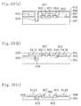
- arsenic ions are selectively implanted into the principal surface portion of a substrate 601 made of GaAs and having a thickness of 150 ⁇ m. Then, heat treatment is conducted to activate the impurity, thereby forming an active layer 602 having a thickness of 0.2 ⁇ m. Thereafter, source/drain electrodes 603 and 604 in ohmic contact with the active layer 602 and a gate electrode 605 in Schottky contact with the active layer 602 are formed in the same way as in the first embodiment. In this manner, an FET including the active layer 602 , the source electrode 603 , the drain electrode 604 and the gate electrode 605 is obtained.
- an etching mask 606 having an opening 606a over a region where a via hole is to be formed and having a thickness of 20 ⁇ m is formed over the principal surface of the substrate 601 .
- the substrate 601 is etched using the etching mask 606 , thereby forming a via hole 607 having a depth of 200 ⁇ m and a bottom in the substrate 601 .
- a cylindrical conductor layer 608 (having a bottom), made of platinum, for example, and having a thickness of 0.5 ⁇ m, is formed over the sidewall and bottom portions of the via hole 607 by electron beam evaporation technique. And the etching mask 606 is removed.
- the source electrode 603 is connected to the sidewall portion of the conductor layer 608 by a known lithography technique and an interconnection layer 609 , made of gold and having a thickness of 0.5 ⁇ m, is formed.
- the back surface portion of the substrate 601 (opposite to the portion where the via hole 607 is formed) is removed such that the bottom portion of the conductor layer 608 is exposed, thereby thinning the substrate 601 .
- a metal electrode 610 made of gold, is deposited over the entire back surface of the substrate 601 .
- the interconnection layer 609 connected to the source electrode 603 is electrically connected to the metal electrode 610 by way of the conductor layer 608 formed in the via hole 607 .
- the steps of forming the via hole 607 in the substrate 601 and forming the conductor layer 608 in the via hole 607 can be performed on the substrate 601 that has not been thinned yet and thus still retains a sufficient mechanical strength. Accordingly, it is possible to prevent the substrate from cracking while the substrate 601 thinned is transported to perform the steps of forming the via hole and the conductor layer. As a result, the production yield of the electronic device can be increased as compared with a conventional method.
- the conductor layer 608 is formed on the sidewall and bottom portions of the via hole 607 by electron beam evaporation technique.
- the conductor layer 608 can be formed in a shorter period of time and much more easily.
- the conductor layer 608 has a bottom and the conductor layer 608 and the metal electrode 610 are connected to each other via the bottom of the conductor layer 608 . Accordingly, the contact resistance between the conductor layer 608 and the metal electrode 610 is reduced.
- the conductor layer 608 formed inside the via hole 607 may be formed in the shape of a shallow column with a recessed portion near the surface thereof, not a cylinder having a bottom.
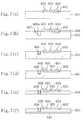
- arsenic ions are selectively implanted into the principal surface portion of a substrate 701 made of GaAs and having a thickness of 150 ⁇ m. Then, heat treatment is conducted to activate the impurity, thereby forming an active layer 702 having a thickness of 0.2 ⁇ m. Thereafter, source/drain electrodes 703 and 704 in ohmic contact with the active layer 702 and a gate electrode 705 in Schottky contact with the active layer 702 are formed in the same way as in the first embodiment. In this manner, an FET including the active layer 702 , the source electrode 703 , the drain electrode 704 and the gate electrode 705 is obtained.
- the source electrode 703 is formed to extend in the direction away from the gate electrode 705 and has an opening 703a over a region where a via hole is to be formed, as in the second embodiment.
- an etching mask 706 having an opening 706a , which communicates with the opening 703a of the source electrode 703 , and having a thickness of 20 ⁇ m is formed over the principal surface of the substrate 701 .
- the substrate 701 is etched using the etching mask 706 , thereby forming a via hole 707 having a depth of 200 ⁇ m and a bottom and communicating with the opening 703a of the source electrode 703 in the substrate 701 .
- One side of the via hole 707 is 20 ⁇ m long.
- a conductor layer 708 having a thickness of 0.5 ⁇ m is formed over the sidewall and bottom portions of the via hole 707 by electron beam evaporation technique or plating technique. And the etching mask 706 is removed.
- the back surface portion of the substrate 701 (opposite to the portion where the via hole 707 is formed) is removed such that the bottom portion of the conductor layer 708 is removed and the sidewall portion thereof is exposed, thereby thinning the substrate 701 .
- a metal electrode 709 made of gold, is deposited over the entire back surface of the substrate 701 .
- the source electrode 703 is electrically connected to the metal electrode 709 by way of the cylindrical conductor layer 708 formed in the via hole 707 .
- the steps of forming the via hole 707 in the substrate 701 and forming the conductor layer 708 in the via hole 707 can be performed on the substrate 701 that has not been thinned yet and thus still retains a sufficient mechanical strength. Accordingly, it is possible to prevent the substrate from cracking while the substrate 701 thinned is transported to perform the steps of forming the via hole and the conductor layer. As a result, the production yield of the electronic device can be increased as compared with a conventional method.
- the source electrode 703 can be connected to the metal electrode 709 by forming the conductor layer 708 in the opening 703a of the source electrode 703 and in the via hole 707 .
- the interconnection layer 109 which is required in the first embodiment for connecting the source electrode 103 to the conductor layer 108 , is not necessary. Accordingly, the process can be simplified as compared with the first embodiment.
- the conductor layer 708 is cylindrical and does not fill in the via hole 707 .
- the time required to form the conductor layer 708 can be shortened.
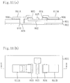
- arsenic ions are selectively implanted into the principal surface portion of a substrate 801 made of GaAs and having a thickness of 150 ⁇ m. Then, heat treatment is conducted to activate the impurity, thereby forming an active layer 802 having a thickness of 0.2 ⁇ m. Thereafter, source/drain electrodes 803 and 804 in ohmic contact with the active layer 802 and a gate electrode 805 in Schottky contact with the active layer 802 are formed in the same way as in the first embodiment. In this manner, an FET including the active layer 802 , the source electrode 803 , the drain electrode 804 and the gate electrode 805 is obtained. Then, a first plating undercoat layer 806 is formed over the entire surface of the substrate 801 by evaporation or sputtering technique.
- an insulator film 807 made of silicon dioxide (SiO 2 ) is deposited over the entire surface of the first plating undercoat layer 806 .
- first and second openings 807a and 807b are formed in respective regions of the insulator film 807 where source-side and drain-side extended interconnections are to be formed. That is to say, these openings 807a and 807b are formed on the left hand side of the source electrode 803 opposite to the gate electrode 805 and on the right hand side of the drain electrode 804 opposite to the gate electrode 805 , respectively.
- an etching mask 808 having an opening 808a over a region where a via hole is to be formed, is formed over the principal surface of the substrate 801 as well as over the insulator film 807 . Then, the first plating undercoat layer 806 and the substrate 801 are etched using the etching mask 808 , thereby forming a via hole 809 having a depth of 200 ⁇ m and a bottom in the substrate 801 . One side of the via hole 809 is 20 ⁇ m long.
- a second plating undercoat layer 810 is formed by evaporation or sputtering technique over the entire surface of the etching mask 808 as well as the inside of the via hole 809 .
- the etching mask 808 is lifted off, thereby leaving the second plating undercoat layer 810 only on the wall and bottom portions of the via hole 809 .
- a metal plating layer is formed over the first and second plating undercoat layers 806 and 810 as well as the inside of the via hole 809 , thereby forming source-side and drain-side extended interconnections 811A and 811B out of the metal plating layer.
- the source-side extended interconnection 811A is formed over the sidewall and bottom portions of the via hole 809 and an upper surface region of the substrate 801
- the drain-side extended interconnection 811B is formed over another upper surface region of the substrate 801 .
- the back surface portion of the substrate 801 (opposite to the portion where the via hole 809 is formed) is removed such that the bottoms of the source-side extended interconnection 811A and the second plating undercoat layer 810 are removed and the sidewall portions of the interconnection 811A and the undercoat layer 810 are exposed, thereby thinning the substrate 801 .
- a metal electrode 812 made of gold, is deposited over the entire back surface of the substrate 801 .
- the source electrode 803 is electrically connected to the metal electrode 812 by way of the source-side extended interconnection 811A formed over the upper surface region of the substrate 801 and the inside of the via hole 809 .
- the steps of forming the via hole 809 in the substrate 801 and forming the source-side and drain-side extended interconnections 811A and 811B can be performed on the substrate 801 that has not been thinned yet and thus still retains a sufficient mechanical strength. Accordingly, it is possible to prevent the substrate 801 from cracking while the substrate 801 thinned is transported to perform the steps of forming the via hole and the interconnections. As a result, the production yield of the electronic device can be increased as compared with a conventional method.
- the source-side and drain-side extended inter-connections 811A and 811B are formed out of the metal plating layer by plating technique using the insulator film 807 as a masking member.
- the source-side extended interconnection 811A connecting the source electrode 803 to the metal electrode 812 and the drain-side extended interconnection 811B connected to the drain electrode 804 can be formed during a single plating process step. As a result, the number of required process steps can be considerably reduced.
- the electrical characteristics of the FET can be tested by connecting a tester electrode to the respective parts of the source-side and drain-side extended interconnections 811A and 811B formed on the principal surface of the substrate 801 . Accordingly, the electrical characteristics of the electronic device, in which the via hole 809 has already been formed, can be performed on the substrate 801 that has not been thinned yet and thus still retains a sufficient mechanical strength. Moreover, the substrate of an electronic device having defective electrical characteristics is not thinned in vain.
- the source-side extended interconnection 811A is cylindrical inside the via hole 809 .
- the interconnection 811A may fill in the via hole 809 .
- any appropriate material that is not eroded owing to etching e.g., photoresist, may be used as a material for the etching mask.
- the conductor layer connecting the source electrode formed on the principal surface of the substrate to the metal electrode formed on the back surface thereof may be made of a conductive metal oxide such as iridium oxide or a conductive metal nitride such as titanium nitride.
- the conductor layer may have a multilayer structure in which a plurality of layers made of these oxides and nitrides are stacked.
- the substrate is made of GaAs.
- the substrate may be a substrate made of any other Group III-V compound semiconductor such as indium phosphide (InP), a silicon substrate, an insulating substrate made of sapphire or the like, or an amorphous substrate such as a glass substrate.
- a substrate including any other device such as a semiconductor laser device, not the FET, may be used.
- the substrate may be thinned by polishing, etching or the like.
Landscapes
- Internal Circuitry In Semiconductor Integrated Circuit Devices (AREA)
- Junction Field-Effect Transistors (AREA)
- Testing Or Measuring Of Semiconductors Or The Like (AREA)
- Electrodes Of Semiconductors (AREA)
Applications Claiming Priority (4)
| Application Number | Priority Date | Filing Date | Title |
|---|---|---|---|
| JP26848697 | 1997-10-01 | ||
| JP268486/97 | 1997-10-01 | ||
| JP183765/98 | 1998-06-30 | ||
| JP18376598A JP3184493B2 (ja) | 1997-10-01 | 1998-06-30 | 電子装置の製造方法 |
Publications (2)
| Publication Number | Publication Date |
|---|---|
| EP0907206A1 true EP0907206A1 (de) | 1999-04-07 |
| EP0907206B1 EP0907206B1 (de) | 2009-03-04 |
Family
ID=26502062
Family Applications (1)
| Application Number | Title | Priority Date | Filing Date |
|---|---|---|---|
| EP98118519A Expired - Lifetime EP0907206B1 (de) | 1997-10-01 | 1998-09-30 | Herstellungsverfahren für ein Substratdurchkontakt |
Country Status (9)
| Country | Link |
|---|---|
| US (1) | US6365513B1 (de) |
| EP (1) | EP0907206B1 (de) |
| JP (1) | JP3184493B2 (de) |
| KR (1) | KR100403481B1 (de) |
| CN (1) | CN1151542C (de) |
| AU (1) | AU741204B2 (de) |
| CA (1) | CA2249062C (de) |
| DE (1) | DE69840620D1 (de) |
| TW (1) | TW396387B (de) |
Cited By (12)
| Publication number | Priority date | Publication date | Assignee | Title |
|---|---|---|---|---|
| WO2001024256A1 (de) * | 1999-09-29 | 2001-04-05 | Infineon Technologies Ag | Verfahren zur dreidimensionalen integration mikroelektronischer systeme |
| EP1259983A1 (de) * | 2000-02-28 | 2002-11-27 | Commissariat A L'energie Atomique | Elektrische verbindung zwischen zwei substratoberflächen und verfahren zu deren realisierung |
| WO2003003423A1 (en) | 2001-06-29 | 2003-01-09 | Xanoptix, Inc. | Topside active optical device apparatus and method |
| EP1077494A3 (de) * | 1999-08-19 | 2003-05-21 | Sharp Kabushiki Kaisha | Heteroübergang-Bipolartransistor und Verfahren zur Herstellung |
| WO2003050850A3 (de) * | 2001-12-12 | 2004-03-11 | Infineon Technologies Ag | Kontaktierung eines halbleiterchips auf einem substrat in flip-chip-ähnlicher technologie |
| WO2005031811A3 (en) * | 2003-09-23 | 2005-06-02 | Micron Technology Inc | Process and integration scheme for fabricating conductive components through-vias and semiconductor components including conductive through-wafer vias |
| EP1391923A4 (de) * | 2002-03-19 | 2005-06-15 | Seiko Epson Corp | Halbleiterbauelement und verfahren zu seiner herstellung, leiterplatte und elektronische vorrichtung |
| US7101792B2 (en) | 2003-10-09 | 2006-09-05 | Micron Technology, Inc. | Methods of plating via interconnects |
| EP1739747A3 (de) * | 2005-06-30 | 2007-08-01 | Shinko Electric Industries Co., Ltd. | Halbleiterchip und Verfahren zur Herstellung |
| US7316063B2 (en) | 2004-01-12 | 2008-01-08 | Micron Technology, Inc. | Methods of fabricating substrates including at least one conductive via |
| EP1677346A3 (de) * | 2001-10-01 | 2008-07-09 | Xsil Technology Limited | Bearbeiten von Substraten, insbesondere von Halbleitersubstraten |
| EP2009688A3 (de) * | 2007-06-29 | 2011-11-09 | Fujitsu Ltd. | Halbleiterbauelement und Verfahren für seine Herstellung |
Families Citing this family (34)
| Publication number | Priority date | Publication date | Assignee | Title |
|---|---|---|---|---|
| JP3736607B2 (ja) * | 2000-01-21 | 2006-01-18 | セイコーエプソン株式会社 | 半導体装置及びその製造方法、回路基板並びに電子機器 |
| US6900534B2 (en) * | 2000-03-16 | 2005-05-31 | Texas Instruments Incorporated | Direct attach chip scale package |
| JP4329235B2 (ja) * | 2000-06-27 | 2009-09-09 | セイコーエプソン株式会社 | 半導体装置及びその製造方法 |
| US20020163072A1 (en) * | 2001-05-01 | 2002-11-07 | Subhash Gupta | Method for bonding wafers to produce stacked integrated circuits |
| JP3834589B2 (ja) * | 2001-06-27 | 2006-10-18 | 株式会社ルネサステクノロジ | 半導体装置の製造方法 |
| US7831151B2 (en) | 2001-06-29 | 2010-11-09 | John Trezza | Redundant optical device array |
| JP4770079B2 (ja) * | 2001-07-12 | 2011-09-07 | 株式会社デンソー | 半導体装置の製造方法 |
| AU2002365151A1 (en) * | 2001-11-07 | 2003-07-09 | The Board Of Trustees Of The University Of Arkansas | Structure and process for packaging rf mems and other devices |
| JP2004031933A (ja) * | 2002-05-09 | 2004-01-29 | Konica Minolta Holdings Inc | 有機薄膜トランジスタの製造方法及び、それにより製造された有機薄膜トランジスタと有機薄膜トランジスタシート |
| US6927073B2 (en) * | 2002-05-16 | 2005-08-09 | Nova Research, Inc. | Methods of fabricating magnetoresistive memory devices |
| US20060097388A1 (en) * | 2002-07-02 | 2006-05-11 | Klaus Breitschwerdt | Electrical system, especially a microelectronic or microelectromechanical high frequency system |
| US6835589B2 (en) * | 2002-11-14 | 2004-12-28 | International Business Machines Corporation | Three-dimensional integrated CMOS-MEMS device and process for making the same |
| JP2004186422A (ja) * | 2002-12-03 | 2004-07-02 | Shinko Electric Ind Co Ltd | 電子部品実装構造及びその製造方法 |
| JP4213478B2 (ja) * | 2003-01-14 | 2009-01-21 | 株式会社ルネサステクノロジ | 半導体装置の製造方法 |
| JP3690407B2 (ja) | 2003-07-31 | 2005-08-31 | セイコーエプソン株式会社 | 半導体装置の製造方法 |
| WO2005053005A2 (en) * | 2003-11-19 | 2005-06-09 | University Of Florida Research Foundation Inc. | A method to contact patterned electrodes on porous substrates and devices thereby |
| JP2005303258A (ja) * | 2004-03-16 | 2005-10-27 | Fujikura Ltd | デバイス及びその製造方法 |
| CN101373747B (zh) * | 2004-03-16 | 2011-06-29 | 株式会社藤仓 | 具有通孔互连的装置及其制造方法 |
| JP2006066412A (ja) * | 2004-08-24 | 2006-03-09 | Mitsubishi Electric Corp | 半導体装置および半導体装置製造方法 |
| JP4311376B2 (ja) | 2005-06-08 | 2009-08-12 | セイコーエプソン株式会社 | 半導体装置、半導体装置の製造方法、電子部品、回路基板及び電子機器 |
| US7307348B2 (en) * | 2005-12-07 | 2007-12-11 | Micron Technology, Inc. | Semiconductor components having through wire interconnects (TWI) |
| US7271047B1 (en) * | 2006-01-06 | 2007-09-18 | Advanced Micro Devices, Inc. | Test structure and method for measuring the resistance of line-end vias |
| EP2002477B1 (de) * | 2006-03-27 | 2011-12-21 | Philips Intellectual Property & Standards GmbH | Herstellungsmethode für eine niederohmige Substratdurchgangsverbindung für Halbleiterträger |
| US7474005B2 (en) * | 2006-05-31 | 2009-01-06 | Alcatel-Lucent Usa Inc. | Microelectronic element chips |
| JP5168933B2 (ja) * | 2007-02-16 | 2013-03-27 | 富士通株式会社 | 化合物半導体装置の製造方法 |
| KR100885924B1 (ko) * | 2007-08-10 | 2009-02-26 | 삼성전자주식회사 | 묻혀진 도전성 포스트를 포함하는 반도체 패키지 및 그제조방법 |
| JP5431777B2 (ja) * | 2009-04-20 | 2014-03-05 | ルネサスエレクトロニクス株式会社 | 半導体装置の製造方法 |
| US8791016B2 (en) * | 2012-09-25 | 2014-07-29 | International Business Machines Corporation | Through silicon via wafer, contacts and design structures |
| JP5983889B2 (ja) * | 2013-09-27 | 2016-09-06 | 富士電機株式会社 | 半導体装置の製造方法 |
| WO2017069460A2 (ko) * | 2015-10-23 | 2017-04-27 | (주)기가레인 | 고전자이동도 트랜지스터 및 그의 제조방법 |
| WO2017069463A1 (ko) * | 2015-10-23 | 2017-04-27 | (주)기가레인 | 고전자이동도 트랜지스터 및 그의 제조방법 |
| CN105470131A (zh) * | 2015-12-30 | 2016-04-06 | 东莞市青麦田数码科技有限公司 | 一种制作砷化镓基hemt器件背孔的方法 |
| CN107368215B (zh) * | 2017-06-01 | 2020-12-01 | 昆山龙腾光电股份有限公司 | 触控面板及其制备方法、显示装置 |
| CN111266934B (zh) * | 2020-02-29 | 2021-06-25 | 湖南大学 | 一种离子束抛光单片集成Fabry-Pérot腔全彩滤光片大批量制造方法 |
Citations (4)
| Publication number | Priority date | Publication date | Assignee | Title |
|---|---|---|---|---|
| US5243498A (en) * | 1992-05-26 | 1993-09-07 | Motorola, Inc. | Multi-chip semiconductor module and method for making and testing |
| EP0693778A2 (de) * | 1994-07-20 | 1996-01-24 | Mitsubishi Denki Kabushiki Kaisha | Halbleiterteil mit integriertem Kühlkörper |
| US5488253A (en) * | 1993-11-10 | 1996-01-30 | Mitsubishi Denki Kabushiki Kaisha | Semiconductor device |
| US5646067A (en) * | 1995-06-05 | 1997-07-08 | Harris Corporation | Method of bonding wafers having vias including conductive material |
Family Cites Families (3)
| Publication number | Priority date | Publication date | Assignee | Title |
|---|---|---|---|---|
| JPH0215652A (ja) * | 1988-07-01 | 1990-01-19 | Mitsubishi Electric Corp | 半導体装置及びその製造方法 |
| JPH065880A (ja) | 1992-06-18 | 1994-01-14 | Matsushita Electric Ind Co Ltd | 半導体装置の製造方法 |
| JPH0846042A (ja) | 1994-08-03 | 1996-02-16 | Sanyo Electric Co Ltd | バイアホールの形成方法 |
-
1998
- 1998-06-30 JP JP18376598A patent/JP3184493B2/ja not_active Expired - Lifetime
- 1998-09-29 US US09/162,232 patent/US6365513B1/en not_active Expired - Lifetime
- 1998-09-29 CN CNB981201075A patent/CN1151542C/zh not_active Expired - Fee Related
- 1998-09-29 CA CA002249062A patent/CA2249062C/en not_active Expired - Fee Related
- 1998-09-30 TW TW087116222A patent/TW396387B/zh not_active IP Right Cessation
- 1998-09-30 EP EP98118519A patent/EP0907206B1/de not_active Expired - Lifetime
- 1998-09-30 DE DE69840620T patent/DE69840620D1/de not_active Expired - Lifetime
- 1998-10-01 AU AU87874/98A patent/AU741204B2/en not_active Ceased
- 1998-10-01 KR KR10-1998-0041434A patent/KR100403481B1/ko not_active Expired - Lifetime
Patent Citations (4)
| Publication number | Priority date | Publication date | Assignee | Title |
|---|---|---|---|---|
| US5243498A (en) * | 1992-05-26 | 1993-09-07 | Motorola, Inc. | Multi-chip semiconductor module and method for making and testing |
| US5488253A (en) * | 1993-11-10 | 1996-01-30 | Mitsubishi Denki Kabushiki Kaisha | Semiconductor device |
| EP0693778A2 (de) * | 1994-07-20 | 1996-01-24 | Mitsubishi Denki Kabushiki Kaisha | Halbleiterteil mit integriertem Kühlkörper |
| US5646067A (en) * | 1995-06-05 | 1997-07-08 | Harris Corporation | Method of bonding wafers having vias including conductive material |
Non-Patent Citations (1)
| Title |
|---|
| GULDAN A ET AL: "METHOD FOR PRODUCING VIA-CONNECTIONS IN SEMICONDUCTOR WAFERS USING A COMBINATION OF PLASMA AND CHEMICAL ETCHING", IEEE TRANSACTIONS ON ELECTRON DEVICES, vol. ED-30, no. 10, October 1983 (1983-10-01), pages 1402/1403, XP002048887 * |
Cited By (27)
| Publication number | Priority date | Publication date | Assignee | Title |
|---|---|---|---|---|
| US6844575B2 (en) | 1999-08-19 | 2005-01-18 | Sharp Kabushiki Kaisha | Heterojunction bipolar transistor and method for fabricating the same |
| EP1077494A3 (de) * | 1999-08-19 | 2003-05-21 | Sharp Kabushiki Kaisha | Heteroübergang-Bipolartransistor und Verfahren zur Herstellung |
| US6633075B1 (en) | 1999-08-19 | 2003-10-14 | Sharp Kabushiki Kaisha | Heterojunction bipolar transistor and method for fabricating the same |
| WO2001024256A1 (de) * | 1999-09-29 | 2001-04-05 | Infineon Technologies Ag | Verfahren zur dreidimensionalen integration mikroelektronischer systeme |
| EP1259983A1 (de) * | 2000-02-28 | 2002-11-27 | Commissariat A L'energie Atomique | Elektrische verbindung zwischen zwei substratoberflächen und verfahren zu deren realisierung |
| EP1410425A4 (de) * | 2001-06-29 | 2009-12-09 | Cufer Asset Ltd Llc | Vorrichtung mit oberseitenaktiven optischem bauelement und verfahren |
| WO2003003423A1 (en) | 2001-06-29 | 2003-01-09 | Xanoptix, Inc. | Topside active optical device apparatus and method |
| EP1677346A3 (de) * | 2001-10-01 | 2008-07-09 | Xsil Technology Limited | Bearbeiten von Substraten, insbesondere von Halbleitersubstraten |
| WO2003050850A3 (de) * | 2001-12-12 | 2004-03-11 | Infineon Technologies Ag | Kontaktierung eines halbleiterchips auf einem substrat in flip-chip-ähnlicher technologie |
| DE10161043B4 (de) * | 2001-12-12 | 2005-12-15 | Infineon Technologies Ag | Chipanordnung |
| EP1391923A4 (de) * | 2002-03-19 | 2005-06-15 | Seiko Epson Corp | Halbleiterbauelement und verfahren zu seiner herstellung, leiterplatte und elektronische vorrichtung |
| US7608904B2 (en) | 2003-09-23 | 2009-10-27 | Micron Technology, Inc. | Semiconductor device components with conductive vias and systems including the components |
| US7345350B2 (en) | 2003-09-23 | 2008-03-18 | Micron Technology, Inc. | Process and integration scheme for fabricating conductive components, through-vias and semiconductor components including conductive through-wafer vias |
| US8148263B2 (en) | 2003-09-23 | 2012-04-03 | Micron Technology, Inc. | Methods for forming conductive vias in semiconductor device components |
| WO2005031811A3 (en) * | 2003-09-23 | 2005-06-02 | Micron Technology Inc | Process and integration scheme for fabricating conductive components through-vias and semiconductor components including conductive through-wafer vias |
| US7666788B2 (en) | 2003-09-23 | 2010-02-23 | Micron Technology, Inc. | Methods for forming conductive vias in semiconductor device components |
| US9287207B2 (en) | 2003-09-23 | 2016-03-15 | Micron Technology, Inc. | Methods for forming conductive vias in semiconductor device components |
| US7101792B2 (en) | 2003-10-09 | 2006-09-05 | Micron Technology, Inc. | Methods of plating via interconnects |
| US7701039B2 (en) | 2003-10-09 | 2010-04-20 | Micron Technology, Inc. | Semiconductor devices and in-process semiconductor devices having conductor filled vias |
| US7316063B2 (en) | 2004-01-12 | 2008-01-08 | Micron Technology, Inc. | Methods of fabricating substrates including at least one conductive via |
| US7594322B2 (en) | 2004-01-12 | 2009-09-29 | Micron Technology, Inc. | Methods of fabricating substrates including at least one conductive via |
| US7603772B2 (en) | 2004-01-12 | 2009-10-20 | Micron Technology, Inc. | Methods of fabricating substrates including one or more conductive vias |
| EP1739747A3 (de) * | 2005-06-30 | 2007-08-01 | Shinko Electric Industries Co., Ltd. | Halbleiterchip und Verfahren zur Herstellung |
| US8338289B2 (en) | 2005-06-30 | 2012-12-25 | Shinko Electric Industries Co., Ltd. | Method of manufacturing a semiconductor chip including a semiconductor substrate and a through via provided in a through hole |
| US7843068B2 (en) | 2005-06-30 | 2010-11-30 | Shinko Electric Industries Co., Ltd. | Semiconductor chip and method of manufacturing the same |
| EP2009688A3 (de) * | 2007-06-29 | 2011-11-09 | Fujitsu Ltd. | Halbleiterbauelement und Verfahren für seine Herstellung |
| US8273655B2 (en) | 2007-06-29 | 2012-09-25 | Fujitsu Limited | Semiconductor device and method of manufacturing the same |
Also Published As
| Publication number | Publication date |
|---|---|
| TW396387B (en) | 2000-07-01 |
| DE69840620D1 (de) | 2009-04-16 |
| JPH11168104A (ja) | 1999-06-22 |
| US6365513B1 (en) | 2002-04-02 |
| CN1213844A (zh) | 1999-04-14 |
| KR19990036781A (ko) | 1999-05-25 |
| EP0907206B1 (de) | 2009-03-04 |
| AU741204B2 (en) | 2001-11-22 |
| KR100403481B1 (ko) | 2004-01-28 |
| JP3184493B2 (ja) | 2001-07-09 |
| AU8787498A (en) | 1999-04-22 |
| CA2249062C (en) | 2005-01-11 |
| CA2249062A1 (en) | 1999-04-01 |
| CN1151542C (zh) | 2004-05-26 |
Similar Documents
| Publication | Publication Date | Title |
|---|---|---|
| EP0907206B1 (de) | Herstellungsverfahren für ein Substratdurchkontakt | |
| US6440822B1 (en) | Method of manufacturing semiconductor device with sidewall metal layers | |
| US6627967B2 (en) | Schottky barrier diode | |
| US5812364A (en) | Capacitor | |
| JPH0897375A (ja) | マイクロ波集積回路装置及びその製造方法 | |
| US6790694B2 (en) | High frequency semiconductor module, high frequency semiconductor device and manufacturing method for the same | |
| JP2790033B2 (ja) | 半導体装置 | |
| US6169320B1 (en) | Spiral-shaped inductor structure for monolithic microwave integrated circuits having air gaps in underlying pedestal | |
| JP2803408B2 (ja) | 半導体装置 | |
| US6462419B1 (en) | Semiconductor device and method for manufacturing the same | |
| US20230029763A1 (en) | Interconnect metal openings through dielectric films | |
| US20250357376A1 (en) | Semiconductor Structures With Improved Reliability | |
| JPH09205178A (ja) | 半導体装置及びその製造方法 | |
| US6787871B2 (en) | Integrated schottky barrier diode and manufacturing method thereof | |
| JPS62211962A (ja) | 高周波半導体装置の製造方法 | |
| US20250210409A1 (en) | Device with electrical component formed over a cavity and method therefor | |
| CN100470845C (zh) | 肖特基势垒二极管及其制造方法 | |
| JP2003069048A (ja) | ショットキーバリアダイオードおよびその製造方法 | |
| KR100616049B1 (ko) | 쇼트키 배리어 다이오드 및 그 제조 방법 | |
| US20030141571A1 (en) | Semiconductor device and manufacturing method thereof | |
| JPH07321343A (ja) | 半導体装置およびその製造方法 | |
| JPS61268060A (ja) | 半導体装置の製造方法 | |
| JPH11150113A (ja) | 半導体装置の製造方法 | |
| CN119545863A (zh) | 一种短沟道场效应晶体管、其制备方法及电子器件 | |
| JP2000100935A (ja) | 半導体装置の製造方法 |
Legal Events
| Date | Code | Title | Description |
|---|---|---|---|
| PUAI | Public reference made under article 153(3) epc to a published international application that has entered the european phase |
Free format text: ORIGINAL CODE: 0009012 |
|
| AK | Designated contracting states |
Kind code of ref document: A1 Designated state(s): DE FI FR GB IT NL SE |
|
| AX | Request for extension of the european patent |
Free format text: AL;LT;LV;MK;RO;SI |
|
| 17P | Request for examination filed |
Effective date: 19990826 |
|
| AKX | Designation fees paid |
Free format text: DE FI FR GB IT NL SE |
|
| RAP1 | Party data changed (applicant data changed or rights of an application transferred) |
Owner name: MATSUSHITA ELECTRIC INDUSTRIAL CO., LTD. |
|
| 17Q | First examination report despatched |
Effective date: 20020425 |
|
| RTI1 | Title (correction) |
Free format text: FABRICATION METHOD FOR A SUBSTRATE THROUGH-CONTACT |
|
| GRAP | Despatch of communication of intention to grant a patent |
Free format text: ORIGINAL CODE: EPIDOSNIGR1 |
|
| RAP1 | Party data changed (applicant data changed or rights of an application transferred) |
Owner name: PANASONIC CORPORATION |
|
| GRAS | Grant fee paid |
Free format text: ORIGINAL CODE: EPIDOSNIGR3 |
|
| GRAA | (expected) grant |
Free format text: ORIGINAL CODE: 0009210 |
|
| AK | Designated contracting states |
Kind code of ref document: B1 Designated state(s): DE FI FR GB IT NL SE |
|
| REG | Reference to a national code |
Ref country code: GB Ref legal event code: FG4D |
|
| REF | Corresponds to: |
Ref document number: 69840620 Country of ref document: DE Date of ref document: 20090416 Kind code of ref document: P |
|
| PG25 | Lapsed in a contracting state [announced via postgrant information from national office to epo] |
Ref country code: NL Free format text: LAPSE BECAUSE OF FAILURE TO SUBMIT A TRANSLATION OF THE DESCRIPTION OR TO PAY THE FEE WITHIN THE PRESCRIBED TIME-LIMIT Effective date: 20090304 Ref country code: FI Free format text: LAPSE BECAUSE OF FAILURE TO SUBMIT A TRANSLATION OF THE DESCRIPTION OR TO PAY THE FEE WITHIN THE PRESCRIBED TIME-LIMIT Effective date: 20090304 |
|
| NLV1 | Nl: lapsed or annulled due to failure to fulfill the requirements of art. 29p and 29m of the patents act | ||
| PG25 | Lapsed in a contracting state [announced via postgrant information from national office to epo] |
Ref country code: SE Free format text: LAPSE BECAUSE OF FAILURE TO SUBMIT A TRANSLATION OF THE DESCRIPTION OR TO PAY THE FEE WITHIN THE PRESCRIBED TIME-LIMIT Effective date: 20090604 |
|
| PLBE | No opposition filed within time limit |
Free format text: ORIGINAL CODE: 0009261 |
|
| STAA | Information on the status of an ep patent application or granted ep patent |
Free format text: STATUS: NO OPPOSITION FILED WITHIN TIME LIMIT |
|
| 26N | No opposition filed |
Effective date: 20091207 |
|
| PGFP | Annual fee paid to national office [announced via postgrant information from national office to epo] |
Ref country code: DE Payment date: 20100922 Year of fee payment: 13 |
|
| PG25 | Lapsed in a contracting state [announced via postgrant information from national office to epo] |
Ref country code: IT Free format text: LAPSE BECAUSE OF FAILURE TO SUBMIT A TRANSLATION OF THE DESCRIPTION OR TO PAY THE FEE WITHIN THE PRESCRIBED TIME-LIMIT Effective date: 20090304 |
|
| PGFP | Annual fee paid to national office [announced via postgrant information from national office to epo] |
Ref country code: GB Payment date: 20110928 Year of fee payment: 14 Ref country code: FR Payment date: 20110922 Year of fee payment: 14 |
|
| GBPC | Gb: european patent ceased through non-payment of renewal fee |
Effective date: 20120930 |
|
| REG | Reference to a national code |
Ref country code: FR Ref legal event code: ST Effective date: 20130531 |
|
| PG25 | Lapsed in a contracting state [announced via postgrant information from national office to epo] |
Ref country code: GB Free format text: LAPSE BECAUSE OF NON-PAYMENT OF DUE FEES Effective date: 20120930 Ref country code: DE Free format text: LAPSE BECAUSE OF NON-PAYMENT OF DUE FEES Effective date: 20130403 |
|
| PG25 | Lapsed in a contracting state [announced via postgrant information from national office to epo] |
Ref country code: FR Free format text: LAPSE BECAUSE OF NON-PAYMENT OF DUE FEES Effective date: 20121001 |
|
| REG | Reference to a national code |
Ref country code: DE Ref legal event code: R119 Ref document number: 69840620 Country of ref document: DE Effective date: 20130403 |