EP0907251B1 - Circuit de retard synchrone - Google Patents
Circuit de retard synchrone Download PDFInfo
- Publication number
- EP0907251B1 EP0907251B1 EP98118741A EP98118741A EP0907251B1 EP 0907251 B1 EP0907251 B1 EP 0907251B1 EP 98118741 A EP98118741 A EP 98118741A EP 98118741 A EP98118741 A EP 98118741A EP 0907251 B1 EP0907251 B1 EP 0907251B1
- Authority
- EP
- European Patent Office
- Prior art keywords
- delay circuit
- clock
- circuit array
- delay
- array
- Prior art date
- Legal status (The legal status is an assumption and is not a legal conclusion. Google has not performed a legal analysis and makes no representation as to the accuracy of the status listed.)
- Expired - Lifetime
Links
- 230000001360 synchronised effect Effects 0.000 title claims description 86
- 239000000872 buffer Substances 0.000 claims description 98
- 230000002250 progressing effect Effects 0.000 claims description 50
- 238000003491 array Methods 0.000 claims description 29
- 230000003111 delayed effect Effects 0.000 claims description 2
- 238000010276 construction Methods 0.000 description 22
- 238000010586 diagram Methods 0.000 description 21
- 238000012546 transfer Methods 0.000 description 19
- 238000013461 design Methods 0.000 description 12
- 238000005259 measurement Methods 0.000 description 11
- 238000000034 method Methods 0.000 description 10
- 238000012986 modification Methods 0.000 description 3
- 230000004048 modification Effects 0.000 description 3
- 101150110971 CIN7 gene Proteins 0.000 description 1
- 101100286980 Daucus carota INV2 gene Proteins 0.000 description 1
- 101150110298 INV1 gene Proteins 0.000 description 1
- 101100397044 Xenopus laevis invs-a gene Proteins 0.000 description 1
- 101100397045 Xenopus laevis invs-b gene Proteins 0.000 description 1
- 239000004065 semiconductor Substances 0.000 description 1
Images








Classifications
-
- H—ELECTRICITY
- H03—ELECTRONIC CIRCUITRY
- H03K—PULSE TECHNIQUE
- H03K5/00—Manipulating of pulses not covered by one of the other main groups of this subclass
- H03K5/13—Arrangements having a single output and transforming input signals into pulses delivered at desired time intervals
- H03K5/133—Arrangements having a single output and transforming input signals into pulses delivered at desired time intervals using a chain of active delay devices
-
- H—ELECTRICITY
- H03—ELECTRONIC CIRCUITRY
- H03K—PULSE TECHNIQUE
- H03K5/00—Manipulating of pulses not covered by one of the other main groups of this subclass
- H03K5/13—Arrangements having a single output and transforming input signals into pulses delivered at desired time intervals
- H03K5/135—Arrangements having a single output and transforming input signals into pulses delivered at desired time intervals by the use of time reference signals, e.g. clock signals
Definitions
- the present invention relates to a semiconductor integrated circuit, and more specifically to a control circuit for a clock signal.
- a synchronous delay circuit capable of removing a clock skew in a synchronizing time of a short time length is used in a high speed synchronous circuit, from the viewpoint of a simple circuit construction and a small current consumption.
- the following documents can be referred to:
- the document US-A-5 245 231 also disclose an example of a synchronous delay circuit.
- the prior art synchronous delay circuit includes two delay circuit arrays composed of a delay circuit array 901 used for measuring a predetermined time difference and a delay circuit array 902 for reproducing the measured delay time, and also includes a dummy delay circuit 905 having a delay time td1+td2 corresponding to the sum of respective delay times td1 and td2 of an input buffer 903 and a clock driver 904.
- a dummy delay circuit 905 having a delay time td1+td2 corresponding to the sum of respective delay times td1 and td2 of an input buffer 903 and a clock driver 904.
- the dummy delay circuit 905 includes an input buffer dummy 905A which is completely the same as that input buffer, and a clock driver dummy 905B, in order to equalize the delay time equal to the delay times td1 and td2 of the input buffer 903 and the clock driver 904.
- the delay circuit array 901 and the delay circuit array 902 are formed of delay circuit arrays having the same delay time.
- the purpose of the delay circuit array 901 and the delay circuit array 902 is to measure a predetermined period of time by means of the delay circuit array 901 and to reproduce the predetermined of time of by means of the delay circuit array 902. Namely, during a period of time to be measured, a signal is progressed in the delay circuit array 901, and a period of time equal to the measuring period is reproduced by causing a signal to pass through delay elements of the same number as that of the delay elements through which the first named signal has progressed.
- a system in which a signal is caused to pass in the delay circuit array 902 the delay elements of the same number as that of the delay elements through which a signal has progressed in the delay circuit array 901, can be classified to two, on the basis of the signal progressing directions of the delay circuit array 901 and the delay circuit array 902.
- this system can also divided into two, on the basis of which of an end of the path and the whole of the path is selected for determining the length of the delay circuit array 902. Therefore, it can be classified into four types.
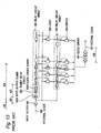
- the system is classified on the basis of the signal progressing directions of the delay circuit array 901 and the delay circuit array 902, it is classified into one in which as shown in Fig. 12 and Fig .13 , the respective signal progressing directions of the delay circuit array 901 and the delay circuit array 902 are the same, and the number of delay elements in the delay circuit arrays 902 is determined by an output terminal side of the delay circuit array 902, and another in which as shown in Fig. 10 and Fig .11 , the respective signal progressing directions of the delay circuit array 901 and the delay circuit array 902 are opposite to each other, and the number of delay elements in the delay circuit arrays 902 is determined by an input terminal side of the delay circuit array 902,
- Fig. 10 corresponds to the system shown in JP-A-08-237091 ( EP-0 720 291-A2 ), and Fig. 11 corresponds to the system shown in the above referred document (5) IEICE TRANS. ELECTRON., VOL.E79-C, NO.6, JUNE 1996 pp.798-807 .
- Fig. 12 corresponds to the above referred document (3) 1996 Symp. on VLSI Circ. pp.192-193
- Fig. 13 corresponds to the above referred document (2) 1996 Symp. on VLSI Circ. pp.112-113 and the above referred document (4) Proc. of IEEE 1992 CICC (Custom Integrated Circuits Conference) 25.2 .
- an external clock 906 passes through an input buffer 903 and a clock driver 904, and is outputted as an internal clock 907.
- a time difference between the external clock and the internal clock is a sum of a delay time td1 of the input buffer 903 and a delay time td2 of the clock driver 904. Namely, td1+td2 becomes the clock skew.
- the synchronous delay circuit shown in Fig. 15A is the same circuit construction as that shown in Fig. 9
- Fig. 15B shows a timing chart for illustrating an operation of the synchronous delay circuit.
- "A", "B” and “C” show signal waveforms on an output of the input buffer 903, an output of the dummy delay circuit 905 and an output node of the second delay circuit 902, respectively.
- the operation of the synchronous delay circuit requires two periods. A first period is used to measure the delay time tcK-(td1+td2) depending upon the clock period, and to determine the delay length of the delay circuit for reproducing the delay amount of tcK-(td1+td2). A second period is used for use the obtained delay amount of tcK-(td1+td2).
- the dummy delay circuit 905 of the clock driver 904 and the delay circuit array 901 are used.
- tcK from the moment a first pulse of two continuous pulses of the external pulse 906 is outputted from the input buffer 903 to the moment a second pulse of the two continuous pulses synchronous delay circuit is outputted from the input buffer 903, a clock is caused to progress in the dummy delay circuit 905 and the delay circuit array 901.
- the delay time of the dummy delay circuit 905 is td1+td2, the time by which the pulse progresses in the delay circuit array 901 becomes tcK-(td1+td2).
- the delay time of the delay circuit array 902 is set to become equal to tcK-(td1+td2) by the pulse progresses in the delay circuit array 901.
- the method for setting this delay time of the delay circuit array 902 is generally divided into four as mentioned above, but a desired object can be achieved by each of the four method.
- the clock outputted from the input buffer 903 passes through the delay circuit 903 having the delay time of tcK-(td1+td2), and outputted from the clock driver 903 so that an internal clock having the delay time tcK is generated.
- the internal clock 907 having no clock skew is generated with two clock periods.
- the pattern previously designed as the macro becomes only the delay circuit array 901 and the delay circuit array 902, and therefore, it is necessary to ensure a region for the dummy clock driver 905B in a layout. This is very uneconomical.
- the delay amount of the clock driver dummy and the delay amount of the clock driver have a difference in a temperature dependency of the delay time and in a temperature dependency of a power supply voltage, as shown in Figs. 16A and 16B , and it is very difficult to make these characteristics completely coincident with each other. Accordingly, the difference between the delay amount of the clock driver dummy and the delay amount of the original clock driver becomes an error in the skew removal.
- Another object of the present invention is to provide a synchronous delay circuit capable of eliminating a clock skew caused by a difference in delay amount between the clock driver dummy and the original clock driver, even if the delay amount of the clock driver varies upon a temperature change, whereby a high precision and an elevated reliability can be realized.
- a synchronous delay circuit comprising a first delay circuit array allowing a pulse or a pulse edge to progress during a constant time, a second delay circuit array capable of allowing the pulse or the pulse edge to pass by a length in proportion to a length by which the pulse or the pulse edge has progressed in the first delay circuit array, and a circuit means for storing and reproducing the period in which a clock pulse progresses in a clock driver.
- the synchronous delay circuit in accordance with the present invention includes a first delay circuit array (1 in Fig. 1 ) allowing a pulse or a pulse edge to progress during a constant time, a second delay circuit array (2 in Fig. 1 ) capable of allowing the pulse or the pulse edge to pass by a length in proportion to a length by which the pulse or the pulse edge has progressed in the first delay circuit array, and a latch delay circuit (9 in Fig. 1 ) for storing and reproducing the period in which a clock pulse progresses in a clock driver (4 in Fig. 1 ).
- An external clock (5 in Fig. 1 ) is inputted through an input buffer (3 in Fig. 1 ) to the clock driver (4 in Fig.
- the external clock passes through the first and second delay circuit arrays (1 and 2 in Fig. 1 ) and outputted from the second delay circuit array (2 in Fig. 1 ) by the time (tcK-(td1+td2) obtained by subtracting from a clock period tcK the sum of a delay time (td2) of the clock driver (4 in Fig. 1 ) and a delay time (td1) of an input buffer dummy (6 in Fig. 1 ), so as to supply the delayed clock pulse to the first delay circuit array, and further, is supplied through a selector circuit (10 in Fig. 1 ) to the clock driver (4 in Fig. 1 ).
- the internal clock signal can be synchronized with the external clock even if the input clock driver (4 in Fig. 1 ) has any delay time.
- the synchronous delay circuit in accordance with the present invention includes, in addition to a clock driver (20 in Fig. 5 ) and an input buffer (19 in Fig. 5 ), first and second delay circuit arrays (11 and 12 in Fig. 5 ) having signal progressing directions opposite to each other, and an output terminal of the delay circuit array (12 in Fig. 5 ) of the reversed signal progressing direction is determined at a time point where the clock pulse has progressed in the one delay circuit array (11 in Fig. 5 ) by a sum (td2+td1) of a delay time of the clock driver (20 in Fig. 5 ) and a delay time of the input buffer (19 in Fig. 5 ), and an input terminal of the delay circuit array (12 in Fig. 5 ) is determined at a time point where the clock pulse has progressed by one clock period.
- the synchronous delay circuit includes a means (an array of latch circuits 16 and an array of switches 17 in Fig. 5 ) for determining an output terminal of the second delay circuit array (12 in Fig. 5 ) at a time point where the clock pulse outputted from the input buffer (22 in Fig. 5 ) has progressed in the first delay circuit array (11 in Fig. 5 ) by a sum (td2+td1) of a delay time of the clock driver (20 in Fig. 5 ) and a delay time of the input buffer (22 in Fig. 5 ), and a means (an array of transfer gates in Fig. 5 ) for determining an input terminal of the second delay circuit array (11 in Fig.
- the synchronous delay circuit in accordance with the present invention includes, in addition to a clock driver (20 in Fig. 6 ) and an input buffer (19 and 22 in Fig. 6 ), first and second delay circuit arrays (14 and 11 in Fig. 6 ) having the same forward signal progressing direction, and a third delay circuit array (12 in Fig. 6 ) having a reversed signal progressing direction, and an output terminal of the third delay circuit array (12 in Fig. 6 ) is determined at a time point where the clock pulse has progressed in the first delay circuit array (14 in Fig. 6 ) by a sum (td2+td1) of a delay time of the clock driver (20 in Fig.
- the synchronous delay circuit includes a means (16 and 17 in Fig. 6 ) for determining an output terminal of the third delay circuit array (12 in Fig. 6 ) at a time point where the clock pulse outputted from the input buffer (19 in Fig. 6 ) has progressed in the first delay circuit array (14 in Fig. 6 ) by a sum (td2+td1) of a delay time of the clock driver (20 in Fig.
- a means for determining an input terminal of the third delay circuit array (12 in Fig. 6 ) receiving the clock pulse transferred from the second delay circuit array (11 in Fig. 6 ) , at a time point where the clock pulse outputted from the input buffer (19 in Fig. 6 ) has progressed in the second delay circuit array (11 in Fig. 6 ) by one clock period tcK.
- the synchronous delay circuit in accordance with the present invention includes, in addition to a clock driver (20 in Fig. 8 ) and an input buffer (19 and 22 in Fig. 8 ) first and second delay circuit arrays (11 and 12 in Fig. 8 ) having signal progressing directions same to each other, an input terminal of the second delay circuit array (12 in Fig. 8 ) is determined at a time point where the clock pulse has progressed in the first delay circuit array (11 in Fig. 8 ) by a sum (td2+td1) of a delay time of the clock driver (20 in Fig. 8 ) and a delay time of the input buffer (22 in Fig. 8 ), and an output terminal of the second delay circuit array (12 in Fig.
- the synchronous delay circuit includes a means (16 and 17 in Fig. 8 ) for determining an input terminal of the second delay circuit array (12 in Fig. 8 ) for receiving the clock pulsed from the input buffer (19 in Fig. 8 ) at a time point where the clock pulse outputted from the input buffer (19 in Fig. 8 ) has progressed in the first delay circuit array (11 in Fig. 8 ) by a sum (td2+td1) of a delay time of the clock driver (20 in Fig. 8 ) and a delay time of the input buffer (22 in Fig.
- the synchronous delay circuit in accordance with the present invention includes, in addition to a clock driver (20 in Fig. 7 ) and an input buffer (19 and 22 in Fig. 7 ), three delay circuit arrays (14, 11 and 12 in Fig. 7 ) having the same signal progressing directions, and an input terminal of the third delay circuit array (12 in Fig. 7 ) is determined at a time point where the clock pulse has progressed in the first delay circuit array (14 in Fig. 7 ) by a sum (td2+td1) of a delay time of the clock driver (20 in Fig. 7 ) and a delay time of the input buffer (22 in Fig. 7 ), and an output terminal of the third delay circuit array (12 in Fig.
- the synchronous delay circuit includes a means (16 and 17 in Fig. 7 ) for determining an input terminal of the third delay circuit array at a time point where the clock pulse outputted from the input buffer (19 in Fig. 7 ) has progressed in the first delay circuit array (14 in Fig. 7 ) by a sum (td2+td1) of a delay time of the clock driver (20 in Fig. 7 ) and a delay time of the input buffer (22 in Fig. 7 ), and a means (25 and 26 in Fig.
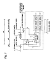
- Fig. 1 is a circuit diagram illustrating a fundamental principle of the synchronous delay circuit in accordance with the present invention
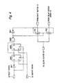
- Fig. 2 is a timing chart illustrating an operation of the synchronous delay circuit in accordance with the present invention.
- the embodiment of the synchronous delay circuit in accordance with the present invention includes a delay circuit array 1 for measuring a constant length of time, a delay circuit array 2 for reproducing the measured delay time, an input buffer 3, a clock driver 4, a latch delay circuit 9 for storing and reproducing the constant time, a selector 10 and an input buffer dummy 6, which are connected as shown.
- the latch delay circuit 9 measures the delay time td2 of the clock driver 4, and measures the clock period tcK by causing a signal to pass through the input buffer dummy 6, the latch delay circuit 9 and the delay circuit array 1.
- a period tV in which the signal progresses in the delay circuit array 1 becomes a time tcK-(td1+td2) obtained by subtracting from the clock period tcK the time obtained by reproducing the delay time td1 of the input buffer dummy 6 and the delay time td2 of the clock driver 45 by the latch delay circuit 9. Accordingly, the delay time tV reproduced in the delay circuit array 2 becomes tcK-(td1+td2).
- the delay circuit arrays 1 and 2, the latch delay circuit 9 and the selector 10 are realized as a synchronous delay circuit macro 8.
- the delay time of the clock driver is stored and reproduced in the latch delay circuit 9. Therefore, a clock driver dummy becomes unnecessary, and the synchronous delay circuit macro 8 can be applied to a clock driver having any delay time.
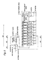
- Fig. 3 is a circuit diagram illustrating the construction of a first embodiment of the synchronous delay circuit in accordance with the present invention.
- the shown embodiment includes input buffers 19 and 22, a clock driver 20, a selector 23, a pair of delay circuit arrays in a forward signal progressing direction and in a reversed signal progressing direction, respectively, and a latch delay circuit 13.
- the forward signal progressing direction delay circuit array and the reversed signal progressing direction delay circuit array are constituted of a delay circuit array 11 for measurement and a delay circuit array 12 for reproducing the measured period.
- the latch circuit 13 includes a delay circuit array 14 for measurement, a delay circuit array 15 for reproducing the measured period, and an array of latch circuits 16 and an array of switches 17 for determining a time point (td2) by which the clock pulse progresses in the delay circuit array 14 by a time in which the clock pulse progresses in the clock driver (clock buffer) 20 and an input terminal of the delay circuit array 15.
- the clock pulse is inputted to the delay circuit array 14 having a number of cascaded delay elements.
- a latch circuit (hatched in the drawing) positioned at a position where the clock pulse progresses in the delay circuit array 14 by a delay time (td2) of the clock driver 20, is enabled.
- the clock pulse outputted from the input buffer 22 progresses in a number of cascaded delay elements of the delay circuit array 11, and when a next clock pulse is outputted from the input buffer 19, the clock pulse progressing in the delay circuit array 11 is transferred to the delay circuit array 12 (composed of a number of cascaded delay elements) through a selected one of an array of transfer gates, since the array of transfer gates are connected between the cascaded delay elements of the delay circuit array 11 and the corresponding cascaded delay elements of the delay circuit array 12, respectively, and are controlled in common by the output of the input buffer 19.
- JP-A-08-237091 EP-0 720 291-A2
- Fig. 11 The detail of the delay circuit arrays 11 and 12 and the array of transfer gates will be referred to the disclosure of JP-A-08-237091 ( EP-0 720 291-A2 ).
- the length of time in which the external clock 18 propagates through the input buffer 19, the latch delay circuit 13, the two delay circuit arrays and the clock driver 20 so that it is outputted as the internal clock 21, requires just two clocks, and therefore, no substantial slew exists between the external clock and the internal clock.
- the circuit having no clock skew is switched from the ordinary clock by the selector 23.
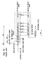
- FIG. 4 A circuit diagram of one example of the construction of the selector 23 shown in Fig. 3 is shown in Fig. 4 .
- the shown selector includes a D-type flipflop D/FF1 with a reset function, having an data input terminal D receiving from an inverter INV1 an inverted signal of a reset signal 24, and another D-type flipflop D/FF2 with a reset function, having an data input terminal D connected to a Q output of the D-type flipflop D/FF1.
- the output clock 21 is supplied in common to a clock terminal C of D/FF1 and D/FF2.
- the selector also includes an NAND gate NAND receiving the Q output of the D-type flipflop D/FF1 and a Q output of the D-type flipflop D/FF2, CMOS transfer gates TG1 and TG2 receiving the output of the input buffer 19 and the output of the delay circuit array 12, respectively.
- a gate of an NMOS transistor of the transfer gate TG1 and a gate of a PMOS transistor of the transfer gate TG2 are connected in common to an output of the NAND gate NAND, and a gate of a PMOS transistor of the transfer gate TG1 and a gate of an NMOS transistor of the transfer gate TG2 are connected in common to receive from an inverter INV2 an inverted signal of the output of the NAND gate NAND.
- the transfer gates TG1 and TG2 are controlled to switch from the output of the input buffer 19 to the output of the delay circuit array 12 with two clocks (two output clocks 21) after the reset signal 24.
- the reset signal 24 is activated to a high level for example at a power-on time, so that D/FF1 and D/FF2 are reset, with the result that the transfer gate TG2 is turned off and the transfer gate TG1 is turned on so as to select the output of the input buffer 19 so that the clock signal is supplied to the clock buffer (driver) 20.
- both the inputs of the NAND gates NAND are brought to the high level, so that the output of the NAND gate NAND is brought to the low level, with the result that the transfer gate TG1 is turned off and the transfer gate TG2 is turned on so as to select the output of the delay circuit 12 so that the output of the delay circuit 12 is supplied to the clock buffer 20.
- Fig. 5 is a circuit diagram illustrating the construction of a second embodiment of the synchronous delay circuit in accordance with the present invention.
- the second embodiment includes, in addition to the clock driver (clock buffer) 2, the input buffers 19 and 22 and the selector 23, a forward signal progressing direction delay circuit array 11 for measurement, a reversed signal progressing direction delay circuit array 12 for reproducing the measured period, and a latch delay circuit 13.
- the latch delay circuit is not clearly indicated, but the delay circuit array 14 for the measurement and the delay circuit array 15 for reproducing the measured period in the latch delay circuit 13 shown in Fig. 3 are in common to the delay circuit array 11 for the measurement and the delay circuit array 12 for reproducing the measured period
- An array of stitches 17 and an array of latch circuits 16 determine an output terminal of the reversed signal progressing direction delay circuit array 12 at a time point (td2+td1) where the clock pulse has progressed in the measuring delay circuit array 11 by the delay times of the clock driver 20 and the input buffer 22.
- This system is the system in which the delay circuit array 11 and the delay circuit array 12 for reproducing the measured period are located in opposite signal progressing directions to each other, and the clock pulse progresses in the delay circuit array 11 and is transferred to the delay circuit array 12 through a transfer circuit (transfer gate hatched in Fig. 5 ) when a next clock pulse is outputted from the input buffer 19 is outputted.
- This system corresponds to the system disclosed by JP-A-08-237091 ( EP-0 720 291-A2 ), and therefore, the detail should be referred to the disclosure of JP-A-08-237091 ( EP-0 720 291-A2 ).
- the length of time in which the external clock 18 propagates through the input buffer 19, the latch delay circuit 13, the two delay circuit arrays 11 and 12 and the clock driver 20 so that it is outputted as the internal clock 21, requires just two clocks, and therefore, no substantial slew exists between the external clock and the internal clock.
- Fig. 6 is a circuit diagram illustrating the construction of a third embodiment of the synchronous delay circuit in accordance with the present invention.
- the third embodiment includes, in addition to the clock driver (clock buffer) 2, the input buffers 19 and 22 and the selector 23, a forward signal progressing direction delay circuit array 11 for measurement, a reversed signal progressing direction delay circuit array 12 for reproducing the measured period, and a latch delay circuit 13.
- the latch delay circuit is not clearly indicated, but the delay circuit array 15 for reproducing the measured period in the latch delay circuit 13 shown in Fig. 3 is in common to the delay circuit array 12 for reproducing the measured period
- the latch delay circuit 13 in this embodiment includes a delay circuit array 14 for measurement.
- An array of switches 17 and an array of latch circuits 16 determine an output terminal of the reversed signal progressing direction delay circuit array 12 at a time point (td2+td1) where the clock pulse has progressed in the measuring delay circuit array 14 by the delay times of the clock driver 20 and the input buffer 22.
- This system is the system in which the delay circuit array 11 and the delay circuit array 12 for reproducing the measured period are located in opposite signal progressing directions to each other, and the clock pulse progresses in the delay circuit array 11 and is transferred to the delay circuit array 12 through a transfer circuit (transfer gate hatched in Fig. 6 ) when a next clock pulse is outputted from the input buffer 19 is outputted.
- This system corresponds to the system disclosed by JP-A-08-237091 ( EP-0 720 291-A2 ), and therefore, the detail should be referred to the disclosure of JP-A-08-237091 ( EP-0 720 291-A2 ).
- the length of time in which the external clock 18 propagates through the input buffer 19, the two delay circuit arrays 11 and 12 and the clock driver 20 so that it is outputted as the internal clock 21, requires just two clocks, and therefore, no substantial slew exists between the external clock and the internal clock.
- Fig. 7 is a circuit diagram illustrating the construction of a fourth embodiment of the synchronous delay circuit in accordance with the present invention.
- the fourth embodiment adopts the system in which the delay circuit array 11 for measuring the clock period tcK and the delay circuit array 12 for reproducing the measured period are located in the same signal progressing direction.
- the clock pulse progresses in the delay circuit array 11, and when a next clock pulse is outputted from the input buffer 19, one is selected from outputs of the delay circuit array 12.
- This system corresponds to the system disclosed by the above referred document (2) 1996 Symp. on VLSI Circ. pp.112-113 and described with reference to Fig. 13 , and therefore, the detail should be referred to the disclosure of the above referred document (2) 1996 Symp. on VLSI Circ. pp.112-113 .
- the latch delay circuit is not clearly indicated, but the delay circuit array 15 for reproducing the measured period in the latch delay circuit 13 shown in Fig. 3 in connection with the first embodiment is in common to the delay circuit array 12 for reproducing the measured period
- this embodiment includes a delay circuit array 14 for measurement, a delay circuit array 11, a delay circuit array 12, an array of switches 17 and an array of latch circuits 16 which determine an input terminal of the forward signal progressing direction delay circuit array 12 at a time point where the clock pulse has progressed in the measuring delay circuit array 14 by the delay times of the clock driver 20 and the input buffer 22, and an array of switches 15 and an array of latch circuits 26 which determine an output terminal of the forward signal progressing direction delay circuit array 12 at a time point where the clock pulse has progressed in the forward signal progressing direction delay circuit array 11 for measuring the clock period tcK.
- Fig. 8 is a circuit diagram illustrating the construction of a fifth embodiment of the synchronous delay circuit in accordance with the present invention.
- the fifth embodiment adopts the system in which the delay circuit array 11 for measuring the clock period tcK and the delay circuit array 12 for reproducing the measured period are located in the same signal progressing direction.
- the clock pulse progresses in the delay circuit array 11, and when a next clock pulse is outputted from the input buffer 19, one is selected from outputs of the delay circuit array 12.
- This system corresponds to the system disclosed by the above referred document (2) 1996 Symp. on VLSI Circ. pp.112-113 and described with reference to Fig. 13 , and therefore, the detail should be referred to the disclosure of the above referred document (2) 1996 Symp. on VLSI Circ. pp.112-113 .
- the latch delay circuit is not clearly indicated, but the delay circuit array 14 for measurement and the delay circuit array 15 for reproducing the measured period in the latch delay circuit 13 shown in Fig. 3 in connection with the first embodiment are in common to the delay circuit array 11 for measurement and the delay circuit array 12 for reproducing the measured period
- an array of switches 17 and an array of latch circuits 16 determine an input terminal of the forward signal progressing direction delay circuit array 12 at a time point (td1+td2) where the clock pulse has progressed in the measuring delay circuit array 11 by the delay times of the clock driver 20 and the input buffer 22, and an array of switches 15 and an array of latch circuits 26 determine an output terminal of the forward signal progressing direction delay circuit array 12 at a time point where the clock pulse has progressed in the forward signal progressing direction delay circuit array 11 for measuring the clock period tcK.
- the synchronous delay circuit in accordance with the present invention is characterized in that the period of the clock is measured by the progressing time of the clock pulse or the clock pulse edge, and the delay amount of the clock driver is stored in the latch circuit. At the time of measuring the clock period, the clock period including the delay amount of the clock driver is measured, but the measured period is reproduced by subtracting the delay amount of the clock driver from the clock period. Thus, the dummy delay circuit of the clock driver is no longer necessary.
- the synchronous delay circuit can be applied to the device such as ASIC having the clock delay amount different from one chip to another, and it is no longer necessary to design the clock driver dummy for each interconnection design modification. Therefore, a working efficiency is elevated, and the chip area can be effectively utilized.
- the delay amount of the actual clock driver is directly measured, even if the delay amount of the actual clock driver varies upon the temperature change of the device, there is not clock skew caused by the difference in delay amount between the clock driver dummy and the original clock driver. Accordingly, precision and reliability can be elevated.
Landscapes
- Physics & Mathematics (AREA)
- Nonlinear Science (AREA)
- Pulse Circuits (AREA)
- Dram (AREA)
- Networks Using Active Elements (AREA)
- Stabilization Of Oscillater, Synchronisation, Frequency Synthesizers (AREA)
- Manipulation Of Pulses (AREA)
Claims (11)
- Circuit à retard synchrone comprenant un premier réseau de circuits à retard (1) permettant à une impulsion d'horloge de progresser pendant un temps constant, un deuxième réseau de circuits à retard (2) capable de permettre à l'impulsion d'horloge de se propager d'une longueur proportionnelle à une longueur de laquelle l'impulsion d'horloge a progressé dans ledit premier réseau de circuits à retard, et des moyens formant circuit (9) pour mémoriser et reproduire la période dans laquelle l'impulsion d'horloge progresse dans un dispositif de commande d'horloge (4),
dans lequel l'impulsion d'horloge est appliquée audit premier réseau de circuits à retard, se propage à travers les premier et deuxième réseaux de circuits à retard et est délivrée par le deuxième réseau de circuits à retard à l'instant obtenu en soustrayant d' une période d' horloge le temps de retard du dispositif de commande d'horloge. - Circuit à retard synchrone selon la revendication 1, comprenant en outre ledit dispositif de commande d'horloge, un circuit tampon d'entrée (3), dans lequel lesdits deux réseaux de circuits à retard (11, 12) ont des directions de progression de signal opposées l'une à l'autre et sont agencés de sorte que l'impulsion d' horloge progresse dans l'un (11) desdits deux réseaux de circuits à retard, et lorsque l'impulsion d'horloge a progressé des temps de retard dudit dispositif de commande d'horloge et dudit circuit tampon d'entrée, une borne de sortie de l'autre (12) desdits deux réseaux de circuits à retard dans une direction de progression de signal inverse est déterminée, et lorsque ladite impulsion d'horloge a progressé dans ledit un (11) desdits deux réseaux de circuits à retard d'une période d'horloge, une borne d'entrée de l'autre (12) desdits deux réseaux de circuits à retard dans une direction de progression de signal inverse est déterminée.
- Circuit à retard synchrone selon la revendication 1, comprenant en outre ledit dispositif de commande d'horloge, un circuit tampon d'entrée (3), dans lequel lesdits premier et deuxième réseaux de circuits à retard comprennent des premier (14) et deuxième (11) réseaux de circuits à retard de direction de progression de signal avant, et un réseau de circuits à retard de direction de progression de signal inverse (12), ces réseaux de circuits à retard étant agencés de sorte que, lorsque l'impulsion d'horloge a progressé dans ledit premier réseau de circuits à retard de direction de progression de signal avant (14) des temps de retard dudit dispositif de commande d'horloge et dudit circuit tampon d'entrée, une borne de sortie dudit réseau de circuits à retard de direction de progression de signal inverse (12) est déterminée, et lorsque ladite impulsion d'horloge a progressé dans ledit deuxième réseau de circuits à retard de direction de progression de signal avant (11) d'une période d'horloge, une borne d'entrée dudit réseau de circuits à retard de direction de progression de signal inverse (12) est déterminée.
- Circuit à retard synchrone selon la revendication 1, comprenant en outre ledit dispositif de commande d'horloge, un circuit tampon d'entrée (3), et dans lequel lesdits premier (11) et deuxième (12) réseaux de circuits à retard ont la même direction de progression de signal, et sont agencés de sorte que, lorsque l'impulsion d'horloge a progressé dans ledit premier réseau de circuits à retard (11) des temps de retard dudit dispositif de commande d'horloge et dudit circuit tampon d'entrée, une borne d'entrée dudit deuxième réseau de circuits à retard (12) est déterminée, et lorsque ladite impulsion d'horloge a progressé dans ledit premier réseau de circuits à retard (11) d'une période d'horloge, une borne de sortie dudit deuxième réseau de circuits à retard (12) est déterminée.
- Circuit à retard synchrone selon la revendication 1, comprenant en outre ledit dispositif de commande d'horloge, un circuit tampon d'entrée (3), et dans lequel lesdits réseaux de circuits à retard comprennent des premier (14), deuxième (11) et troisième (12) réseaux de circuits à retard ayant la même direction de progression de signal avant, et sont agencés de sorte que, lorsque l'impulsion d'horloge a progressé dans ledit premier réseau de circuits à retard (14) des temps de retard dudit dispositif de commande d'horloge et dudit circuit tampon d'entrée, une borne d'entrée dudit troisième réseau de circuits à retard (12) est déterminée, et lorsque ladite impulsion d'horloge a progressé dans ledit deuxième réseau de circuits à retard (11) d'une période d'horloge, une borne de sortie dudit troisième réseau de circuits à retard (12) est déterminée.
- Circuit à retard synchrone selon la revendication 1, configuré pour recevoir une horloge externe (5) dans un circuit tampon d'entrée (3) et pour synchroniser un signal d'horloge interne (7) délivré par ledit dispositif de commande d'horloge (4) avec ladite horloge externe,
dans lequel lesdits moyens formant circuit (9) reçoivent ladite impulsion d'horloge dudit circuit tampon d'entrée et une sortie dudit dispositif de commande d'horloge, pour mémoriser la période dans laquelle ladite impulsion d'horloge progresse dans ledit dispositif de commande d'horloge, lesdits moyens formant circuit retardent ladite impulsion d'horloge provenant dudit circuit tampon d'entrée d'un temps de retard obtenu en additionnant un temps de retard (td2) dudit dispositif de commande d'horloge et un temps de retard (td1) dudit circuit tampon d'entrée, de manière à délivrer l'impulsion d'horloge retardée audit premier réseau de circuits à retard ; et le circuit à retard synchrone comprend en outre :un circuit de sélection (10) pour sélectionner l'un dudit signal d'horloge dudit circuit tampon d'entrée et d'un signal de sortie dudit deuxième réseau de circuits à retard, pour délivrer le signal sélectionné audit dispositif de commande d'horloge en tant que signal d'horloge,dans lequel, à un instant auquel ladite impulsion d'horloge délivrée par lesdits moyens formant circuit a progressé dans ledit premier réseau de circuits à retard d'un temps (tcK-(td1+td2)) obtenu en soustrayant (td1+td2) d'une période d'horloge tcK, ladite impulsion d'horloge est transférée audit deuxième réseau de circuits à retard, de sorte qu'après la progression de ladite impulsion d'horloge dans ledit deuxième réseau de circuits à retard du temps (tcK-(td1+td2)), ladite impulsion d'horloge est sortie dudit deuxième réseau de circuits à retard et est délivrée par l'intermédiaire dudit circuit de sélection audit dispositif de commande d'horloge, moyennant quoi ledit signal d'horloge interne délivré par ledit dispositif de commande d'horloge est synchronisé avec ladite horloge externe appliquée audit circuit tampon d'entrée. - Circuit à retard synchrone selon la revendication 6, dans lequel lesdits moyens formant circuit comprennent un troisième réseau de circuits à retard pour amener ladite impulsion d'horloge à progresser pendant un temps constant, et un quatrième réseau de circuits à retard capable de permettre à ladite impulsion d'horloge de se propager d'une longueur proportionnelle à une longueur de laquelle ladite impulsion d'horloge a progressé dans ledit troisième réseau de circuits à retard ; et
dans lequel le circuit à retard synchrone comprend en outre des moyens pour mémoriser une position à laquelle un signal à délivrer audit dispositif de commande d'horloge est appliqué audit troisième réseau de circuits à retard pour progresser dans ledit troisième réseau de circuits à retard et a progressé du temps de retard (td2) du dispositif de commande d'horloge, et pour sélectionner une borne d'entrée dudit quatrième réseau de circuits à retard correspondant à ladite position,
de sorte que ladite impulsion d'horloge dudit circuit tampon d'entrée est délivrée à ladite borne d'entrée sélectionnée dudit quatrième réseau de circuits à retard, et le signal délivré par ledit quatrième réseau de circuits à retard en progressant dans ledit quatrième réseau de circuits à retard est délivré audit premier réseau de circuits à retard par l'intermédiaire d' un faux circuit tampon d' entrée équivalent audit circuit tampon d'entrée pour avoir un temps de retard td1. - Circuit à retard synchrone selon la revendication 1, configuré pour recevoir une horloge externe (5) dans un circuit tampon d'entrée (3) et pour synchroniser un signal d'horloge interne (7) délivré par ledit dispositif de commande d'horloge (4) avec ladite horloge externe,
dans lequel lesdits premier (1 ou 11) et deuxième (2 ou 12) réseaux de circuits à retard ont des directions de progression de signal opposées l'une à l'autre ; et le circuit à retard synchrone comprend en outre :
des moyens pour déterminer une borne de sortie dudit deuxième réseau de circuits à retard (12) à un instant auquel ladite impulsion d'horloge délivrée par ledit circuit tampon d'entrée a progressé dans ledit premier réseau de circuits à retard (11) d'une somme (td2+td1) d'un temps de retard dudit dispositif de commande d'horloge et d' un temps de retard dudit circuit tampon d'entrée (22) ; et
des moyens pour déterminer une borne d'entrée dudit deuxième réseau de circuits à retard (12) recevant ladite impulsion d'horloge transférée à partir dudit premier réseau de circuits à retard (11), à un instant auquel ladite impulsion d'horloge délivrée par ledit circuit tampon d'entrée (19) a progressé dans ledit premier réseau de circuits à retard (11) d'une période d'horloge tcK. - Circuit à retard synchrone selon la revendication 8, le circuit à retard synchrone comprenant en outre :un troisième réseau de circuits à retard (14) ayant la même direction de progression de signal que ledit premier réseau de circuits à retard ;dans lequel lesdits moyens pour déterminer une borne de sortie dudit deuxième réseau de circuits à retard (12) ont été adaptés pour déterminer une borne de sortie dudit deuxième réseau de circuits à retard (12), à un instant auquel ladite impulsion d'horloge délivrée par ledit circuit tampon d'entrée (22) a progressé dans ledit troisième réseau de circuits à retard (14) d'une somme (td2+td1) d'un temps de retard dudit dispositif de commande d'horloge et d'un temps de retard dudit circuit tampon d'entrée.
- Circuit à retard synchrone selon la revendication 1,
dans lequel lesdits premier (11) et deuxième (12) réseaux de circuits à retard ont la même direction de traitement de signal,
ledit circuit à retard synchrone comprenant en outre :
des moyens pour déterminer une borne d'entrée dudit deuxième réseau de circuits à retard (12) à un instant auquel ladite impulsion d'horloge délivrée par ledit circuit tampon d'entrée a progressé dans ledit premier réseau de circuits à retard (11) d'une somme (td2+td1) d'un temps de retard dudit dispositif de commande d'horloge et d' un temps de retard dudit circuit tampon d'entrée ; et
des moyens pour déterminer une borne de sortie dudit deuxième réseau de circuits à retard (12), à un instant auquel ladite impulsion d'horloge délivrée par ledit circuit tampon d'entrée a progressé dans ledit premier réseau de circuits à retard (11) d'une période d' horloge tcK. - Circuit à retard synchrone selon la revendication 10, configuré pour recevoir une horloge externe dans un circuit tampon d'entrée et pour synchroniser un signal d'horloge interne délivré par un dispositif de commande d'horloge avec ladite horloge externe, le circuit à retard synchrone comprenant en outre :un troisième réseau de circuits à retard (14) ayant les mêmes directions de progression de signal que ledit premier réseau de circuits à retard ;lesdits moyens pour déterminer une borne d'entrée ont été adaptés pour déterminer une borne d'entrée dudit deuxième réseau de circuits à retard (12) à un instant auquel ladite impulsion d'horloge délivrée par ledit circuit tampon d'entrée a progressé dans ledit troisième réseau de circuits à retard (14) d'une somme (td2+td1) d'un temps de retard dudit dispositif de commande d'horloge et d'un temps de retard dudit circuit tampon d'entrée.
Applications Claiming Priority (3)
| Application Number | Priority Date | Filing Date | Title |
|---|---|---|---|
| JP28774397A JP3434682B2 (ja) | 1997-10-03 | 1997-10-03 | 同期遅延回路 |
| JP28774397 | 1997-10-03 | ||
| JP287743/97 | 1997-10-03 |
Publications (3)
| Publication Number | Publication Date |
|---|---|
| EP0907251A2 EP0907251A2 (fr) | 1999-04-07 |
| EP0907251A3 EP0907251A3 (fr) | 2001-01-17 |
| EP0907251B1 true EP0907251B1 (fr) | 2009-07-22 |
Family
ID=17721190
Family Applications (1)
| Application Number | Title | Priority Date | Filing Date |
|---|---|---|---|
| EP98118741A Expired - Lifetime EP0907251B1 (fr) | 1997-10-03 | 1998-10-05 | Circuit de retard synchrone |
Country Status (7)
| Country | Link |
|---|---|
| US (1) | US6222408B1 (fr) |
| EP (1) | EP0907251B1 (fr) |
| JP (1) | JP3434682B2 (fr) |
| KR (1) | KR100279389B1 (fr) |
| CN (1) | CN1144367C (fr) |
| DE (1) | DE69840993D1 (fr) |
| TW (1) | TW429682B (fr) |
Families Citing this family (11)
| Publication number | Priority date | Publication date | Assignee | Title |
|---|---|---|---|---|
| JP3415444B2 (ja) | 1998-06-12 | 2003-06-09 | Necエレクトロニクス株式会社 | クロック制御方法および回路 |
| JP3386031B2 (ja) * | 2000-03-06 | 2003-03-10 | 日本電気株式会社 | 同期遅延回路及び半導体集積回路装置 |
| US6930525B2 (en) * | 2002-06-12 | 2005-08-16 | Micron Technology, Inc. | Methods and apparatus for delay circuit |
| US6903592B2 (en) * | 2003-01-22 | 2005-06-07 | Promos Technologies Inc. | Limited variable width internal clock generation |
| JP4480341B2 (ja) * | 2003-04-10 | 2010-06-16 | 日立プラズマディスプレイ株式会社 | プラズマディスプレイ装置 |
| US6856270B1 (en) * | 2004-01-29 | 2005-02-15 | International Business Machines Corporation | Pipeline array |
| US7084686B2 (en) * | 2004-05-25 | 2006-08-01 | Micron Technology, Inc. | System and method for open-loop synthesis of output clock signals having a selected phase relative to an input clock signal |
| JP4425722B2 (ja) | 2004-06-18 | 2010-03-03 | Necエレクトロニクス株式会社 | Smd任意逓倍回路 |
| JP2006067190A (ja) | 2004-08-26 | 2006-03-09 | Nec Electronics Corp | クロック生成回路 |
| US7078951B2 (en) * | 2004-08-27 | 2006-07-18 | Micron Technology, Inc. | System and method for reduced power open-loop synthesis of output clock signals having a selected phase relative to an input clock signal |
| JP2017220063A (ja) * | 2016-06-08 | 2017-12-14 | キヤノン株式会社 | 半導体集積回路 |
Family Cites Families (3)
| Publication number | Priority date | Publication date | Assignee | Title |
|---|---|---|---|---|
| US5245231A (en) | 1991-12-30 | 1993-09-14 | Dell Usa, L.P. | Integrated delay line |
| TW288232B (fr) * | 1994-12-20 | 1996-10-11 | Nippon Electric Co | |
| JP3672056B2 (ja) * | 1995-08-18 | 2005-07-13 | 松下電器産業株式会社 | タイミング信号発生回路 |
-
1997
- 1997-10-03 JP JP28774397A patent/JP3434682B2/ja not_active Expired - Fee Related
-
1998
- 1998-10-01 TW TW087116415A patent/TW429682B/zh not_active IP Right Cessation
- 1998-10-02 KR KR1019980041607A patent/KR100279389B1/ko not_active Expired - Fee Related
- 1998-10-05 CN CNB981201172A patent/CN1144367C/zh not_active Expired - Fee Related
- 1998-10-05 US US09/166,177 patent/US6222408B1/en not_active Expired - Lifetime
- 1998-10-05 DE DE69840993T patent/DE69840993D1/de not_active Expired - Lifetime
- 1998-10-05 EP EP98118741A patent/EP0907251B1/fr not_active Expired - Lifetime
Also Published As
| Publication number | Publication date |
|---|---|
| DE69840993D1 (de) | 2009-09-03 |
| US6222408B1 (en) | 2001-04-24 |
| TW429682B (en) | 2001-04-11 |
| KR19990036833A (ko) | 1999-05-25 |
| CN1213900A (zh) | 1999-04-14 |
| JPH11112309A (ja) | 1999-04-23 |
| EP0907251A3 (fr) | 2001-01-17 |
| KR100279389B1 (ko) | 2001-02-01 |
| JP3434682B2 (ja) | 2003-08-11 |
| EP0907251A2 (fr) | 1999-04-07 |
| CN1144367C (zh) | 2004-03-31 |
Similar Documents
| Publication | Publication Date | Title |
|---|---|---|
| US8484523B2 (en) | Sequential digital circuitry with test scan | |
| EP0909031B1 (fr) | Circuit de retard synchrone | |
| EP0907251B1 (fr) | Circuit de retard synchrone | |
| JPH0752373B2 (ja) | クロックされたロード・イネーブル信号及びアウトプット・イネーブル信号の供給回路を有する集積回路 | |
| US6640310B2 (en) | Clock system for multiple component system | |
| KR19990014312A (ko) | 반도체 기억장치 | |
| US5535343A (en) | Method and apparatus for generating write signals | |
| KR100395467B1 (ko) | 동기 지연회로 및 반도체 집적회로 장치 | |
| US5742190A (en) | Method and apparatus for clocking latches in a system having both pulse latches and two-phase latches | |
| US6792554B2 (en) | Method and system for synchronously transferring data between clock domains sourced by the same clock | |
| US7200197B2 (en) | Semiconductor integrated circuit | |
| USH1796H (en) | Method and circuit for eliminating hold time violations in synchronous circuits | |
| US6150861A (en) | Flip-flop | |
| US6590795B2 (en) | High speed data capture circuit for a digital device | |
| JP4741122B2 (ja) | 半導体装置及びデータ転送方法 | |
| JP2646561B2 (ja) | クロック分配回路 | |
| KR100303996B1 (ko) | 멀티위상 검출장치 | |
| JP2004127012A (ja) | 同期式回路およびその設計方法 | |
| JP3703655B2 (ja) | タイミング信号発生回路 | |
| JPH0818438A (ja) | ゲートアレー構成半導体装置 | |
| KR19980050372A (ko) | 데이타 전송 동기용 클럭 발생장치 | |
| Chaney et al. | A Digital Phase Adjustment Circuit for ATM and ATM-Like Data Formats," | |
| JPH05157807A (ja) | 記憶回路 | |
| Gray et al. | Design Examples | |
| JP2004207530A (ja) | 半導体集積回路及びそのレイアウト設計方法 |
Legal Events
| Date | Code | Title | Description |
|---|---|---|---|
| PUAI | Public reference made under article 153(3) epc to a published international application that has entered the european phase |
Free format text: ORIGINAL CODE: 0009012 |
|
| AK | Designated contracting states |
Kind code of ref document: A2 Designated state(s): DE FR GB |
|
| AX | Request for extension of the european patent |
Free format text: AL;LT;LV;MK;RO;SI |
|
| PUAL | Search report despatched |
Free format text: ORIGINAL CODE: 0009013 |
|
| AK | Designated contracting states |
Kind code of ref document: A3 Designated state(s): AT BE CH CY DE DK ES FI FR GB GR IE IT LI LU MC NL PT SE |
|
| AX | Request for extension of the european patent |
Free format text: AL;LT;LV;MK;RO;SI |
|
| RIC1 | Information provided on ipc code assigned before grant |
Free format text: 7H 03K 5/13 A, 7H 04L 7/033 B, 7G 06F 1/10 B |
|
| 17P | Request for examination filed |
Effective date: 20010511 |
|
| AKX | Designation fees paid |
Free format text: DE FR GB |
|
| RAP1 | Party data changed (applicant data changed or rights of an application transferred) |
Owner name: NEC ELECTRONICS CORPORATION |
|
| 17Q | First examination report despatched |
Effective date: 20070928 |
|
| GRAP | Despatch of communication of intention to grant a patent |
Free format text: ORIGINAL CODE: EPIDOSNIGR1 |
|
| GRAS | Grant fee paid |
Free format text: ORIGINAL CODE: EPIDOSNIGR3 |
|
| GRAA | (expected) grant |
Free format text: ORIGINAL CODE: 0009210 |
|
| AK | Designated contracting states |
Kind code of ref document: B1 Designated state(s): DE FR GB |
|
| REG | Reference to a national code |
Ref country code: GB Ref legal event code: FG4D |
|
| REF | Corresponds to: |
Ref document number: 69840993 Country of ref document: DE Date of ref document: 20090903 Kind code of ref document: P |
|
| PLBE | No opposition filed within time limit |
Free format text: ORIGINAL CODE: 0009261 |
|
| STAA | Information on the status of an ep patent application or granted ep patent |
Free format text: STATUS: NO OPPOSITION FILED WITHIN TIME LIMIT |
|
| 26N | No opposition filed |
Effective date: 20100423 |
|
| REG | Reference to a national code |
Ref country code: FR Ref legal event code: CD |
|
| REG | Reference to a national code |
Ref country code: DE Ref legal event code: R082 Ref document number: 69840993 Country of ref document: DE Representative=s name: BETTEN & RESCH, DE |
|
| REG | Reference to a national code |
Ref country code: DE Ref legal event code: R082 Ref document number: 69840993 Country of ref document: DE Representative=s name: PATENTANWAELTE BETTEN & RESCH, DE Effective date: 20120828 Ref country code: DE Ref legal event code: R081 Ref document number: 69840993 Country of ref document: DE Owner name: RENESAS ELECTRONICS CORPORATION, KAWASAKI-SHI, JP Free format text: FORMER OWNER: NEC ELECTRONICS CORP., KANAGAWA, JP Effective date: 20120828 Ref country code: DE Ref legal event code: R081 Ref document number: 69840993 Country of ref document: DE Owner name: RENESAS ELECTRONICS CORPORATION, JP Free format text: FORMER OWNER: NEC ELECTRONICS CORP., KANAGAWA, JP Effective date: 20120828 |
|
| PGFP | Annual fee paid to national office [announced via postgrant information from national office to epo] |
Ref country code: FR Payment date: 20121018 Year of fee payment: 15 Ref country code: DE Payment date: 20121003 Year of fee payment: 15 |
|
| PGFP | Annual fee paid to national office [announced via postgrant information from national office to epo] |
Ref country code: GB Payment date: 20121003 Year of fee payment: 15 |
|
| GBPC | Gb: european patent ceased through non-payment of renewal fee |
Effective date: 20131005 |
|
| REG | Reference to a national code |
Ref country code: DE Ref legal event code: R119 Ref document number: 69840993 Country of ref document: DE Effective date: 20140501 |
|
| PG25 | Lapsed in a contracting state [announced via postgrant information from national office to epo] |
Ref country code: GB Free format text: LAPSE BECAUSE OF NON-PAYMENT OF DUE FEES Effective date: 20131005 |
|
| REG | Reference to a national code |
Ref country code: FR Ref legal event code: ST Effective date: 20140630 |
|
| PG25 | Lapsed in a contracting state [announced via postgrant information from national office to epo] |
Ref country code: DE Free format text: LAPSE BECAUSE OF NON-PAYMENT OF DUE FEES Effective date: 20140501 Ref country code: FR Free format text: LAPSE BECAUSE OF NON-PAYMENT OF DUE FEES Effective date: 20131031 |