EP0907257A2 - Fehlerkorrektur verschachtelter Datenblöcke - Google Patents
Fehlerkorrektur verschachtelter Datenblöcke Download PDFInfo
- Publication number
- EP0907257A2 EP0907257A2 EP98118429A EP98118429A EP0907257A2 EP 0907257 A2 EP0907257 A2 EP 0907257A2 EP 98118429 A EP98118429 A EP 98118429A EP 98118429 A EP98118429 A EP 98118429A EP 0907257 A2 EP0907257 A2 EP 0907257A2
- Authority
- EP
- European Patent Office
- Prior art keywords
- data
- block
- error correction
- memory
- channels
- Prior art date
- Legal status (The legal status is an assumption and is not a legal conclusion. Google has not performed a legal analysis and makes no representation as to the accuracy of the status listed.)
- Granted
Links
- 230000015654 memory Effects 0.000 claims abstract description 87
- 238000000034 method Methods 0.000 claims abstract description 34
- 230000003287 optical effect Effects 0.000 claims description 20
- 238000001514 detection method Methods 0.000 claims description 6
- 238000012545 processing Methods 0.000 description 93
- 230000007547 defect Effects 0.000 description 7
- 230000001360 synchronised effect Effects 0.000 description 5
- 230000001174 ascending effect Effects 0.000 description 1
- 238000006243 chemical reaction Methods 0.000 description 1
- 238000003780 insertion Methods 0.000 description 1
- 230000037431 insertion Effects 0.000 description 1
- 238000004519 manufacturing process Methods 0.000 description 1
- 230000008707 rearrangement Effects 0.000 description 1
- 230000005236 sound signal Effects 0.000 description 1
Images







Classifications
-
- H—ELECTRICITY
- H03—ELECTRONIC CIRCUITRY
- H03M—CODING; DECODING; CODE CONVERSION IN GENERAL
- H03M13/00—Coding, decoding or code conversion, for error detection or error correction; Coding theory basic assumptions; Coding bounds; Error probability evaluation methods; Channel models; Simulation or testing of codes
- H03M13/65—Purpose and implementation aspects
- H03M13/6566—Implementations concerning memory access contentions
-
- H—ELECTRICITY
- H03—ELECTRONIC CIRCUITRY
- H03M—CODING; DECODING; CODE CONVERSION IN GENERAL
- H03M13/00—Coding, decoding or code conversion, for error detection or error correction; Coding theory basic assumptions; Coding bounds; Error probability evaluation methods; Channel models; Simulation or testing of codes
- H03M13/27—Coding, decoding or code conversion, for error detection or error correction; Coding theory basic assumptions; Coding bounds; Error probability evaluation methods; Channel models; Simulation or testing of codes using interleaving techniques
- H03M13/2703—Coding, decoding or code conversion, for error detection or error correction; Coding theory basic assumptions; Coding bounds; Error probability evaluation methods; Channel models; Simulation or testing of codes using interleaving techniques the interleaver involving at least two directions
-
- H—ELECTRICITY
- H03—ELECTRONIC CIRCUITRY
- H03M—CODING; DECODING; CODE CONVERSION IN GENERAL
- H03M13/00—Coding, decoding or code conversion, for error detection or error correction; Coding theory basic assumptions; Coding bounds; Error probability evaluation methods; Channel models; Simulation or testing of codes
- H03M13/27—Coding, decoding or code conversion, for error detection or error correction; Coding theory basic assumptions; Coding bounds; Error probability evaluation methods; Channel models; Simulation or testing of codes using interleaving techniques
- H03M13/2782—Interleaver implementations, which reduce the amount of required interleaving memory
Definitions
- the present invention relates to a method of generating and processing data by an interleave method capable of processing with a few memories in a digital recording and reproducing system using an optical disk or the like, a medium recording the data, and a data recording apparatus and a reproducing apparatus.
- a storage capacity for every unit area becomes high with an improvement of the high density recording technique in a digital recording and reproducing apparatus to record and reproduce to/from such as an optical disk, a magnetic disk, and a magnetic tape.
- a digital recording and reproducing apparatus to record and reproduce to/from such as an optical disk, a magnetic disk, and a magnetic tape.
- an occurring error can be corrected by adding an error correction code to the recording data against the error generation of the data by the defect of the noise and the medium.
- An "interleave” method is a method of multiplying a plurality of data in which an error correction coding is performed by rearranging the data and the data of the identical error correction code are dispersed in a wide range. Since the error occurred continuously on the recording data series is dispersed by a plurality of error correction codes when performing an interleave, the burst error correction ability becomes high.
- RS code Reed-Solomon code
- the input data is divided by predetermined data unit to arrange in two-dimensional form and constitute a data block.
- An outer code parity produced by the coding of the RS code to each column data in the data block.
- An inner code parity is produced by the coding of the RS code to each row data.
- the error correction block is constituted from data block, the outer code parity and the inner code parity.
- the four error correction blocks are arranged in the side direction according to the number of the interleave blocks.
- FIG. 1 shows a arranged data. Next, data is taken out from this block for each line and after rearranging data according to the necessity, data is output as a recording data.
- FIGS. 2A and 2B show an example of the interleave processing when using a memory.
- a memory is composed of a plurality of banks capable of storing the error correction block.
- the input data is once written into the memory. If an error correction coding to the continuing the input data is performed, the writing to the bank A is stored and data for the one data block to be coded is written until period T3 in period T0. When the writing to the bank A is completed, the error correction coding processing to the bank A data is started in period T4. At the same time, the writing of the input data to the bank B is changed.
- the error correction coding processing and the writing to the memory is sequentially performed.
- the data in which an error correction coding is performed is read from the memory according to the interleave method.
- the data To perform an interleave processing in four blocks, the data must be read from four banks in parallel. Therefore, the read processing from the memory can not be started after period T20 when an error correction coding for the four-bank data from bank A to D is completed.
- the reading ends at period T35. During the reading period, the error correction coding processing and the writing of the input data are performed by advancing the banks.
- the memory from the banks A to D which reading is completed becomes reusable after period T36. After the writing to the bank 1 is completed, the data can be written into the bank A from period T36. Therefore, the number of the minimum memory banks of necessary interleave processing becomes nine.
- the error correction block of the number according to the number of the interleaves is combined and data is replaced in the combined blocks and the interleave is employed to strengthen the burst error correction ability. Therefore, when realizing the interleave processing using the memory, there is a problem the use efficiency of the memory lowers since the period which performs no processing occurs, as the result, the storage capacity necessary to process an interleave increases.
- an object of the present invention is to improve the use efficiency of the memory when realizing the interleave processing using the memory.
- data is divided into the predetermined size of data block and a data block is assigned to a plurality of channels as the unit. Then, a coding of at least two types of the error correction codes is performed every channel.
- the error correction block is constituted by the data block and the check parity generated by the coding processing, and is recorded to the recording medium after multiplying to the data series by adding a different offset for each of the plurality of channels.
- the data read from the recording medium is divided into the plurality of channels, and by adding the offset according to the channel number of the channels, the error correction block is generated.
- the error detection and correction is performed by decoding at least two types of error correction codes to the error correction block and reproduced data is output in order from each channel in a predetermined data block unit.
- the storage capacity which is necessary for the deinterleave processing can be reduced.
- the memory for interleave in the recording device and the memory for deinterleave in the reproducing device can be used efficiently by adding the predetermined offset among the error correction blocks to be interleaved when performing the deinterleave processing among the plurality of error correction blocks. Therefore, the capacity of each memory which becomes necessary can be reduced.
- the digitized picture signal and the audio signal, the various digital data treated in the computer can be recorded to the optical disk.
- FIG. 3 shows a block structure of the optical disk drive.
- the input data to be recorded is input from the input terminal 1 as the digital data.
- the input data is treated by the predetermined size which is called a sector as a unit.
- the input data is once written into a recording memory 2 with the auxiliary information which is added every sector and so on.
- the data in the recording memory 2 is read and is performed the coding processing of an error correction code by a correction encoder 3.
- the check parity generated by the coding processing is added to the recording memory 2.
- the data in performing the error correction coding is read from the recording memory 2.
- the reading of the data from the memory is performed by the order which is different from the writing according to the predetermined interleave method.
- the read data is converted to the signal form which matches the recording characteristics of a optical disk 5 in a modulation section 4.
- a picking-up section 8 inputs the data through a recording amplifier 7.
- the data is recorded to the optical disk 5 by the laser signal output from the picking-up section 8.
- a recording track is formed in a shape of concentricity or spiral.
- a recording position to the optical disk is fixed by controlling the turn of the optical disk 5 and the position of the picking-up section 8 by a servo section 9.
- the reproduction of the data recorded to the optical disk 5 is performed by the following procedure.
- the optical disk to be reproduced may be the read-only disk in which data is recorded when manufacturing a disk and the disk including a region capable of recording and a read-only region in addition to the recordable and reproducable optical disk.
- the signal recorded to the optical disk 5 is read by the laser light by turning the optical disk 5 and controlling the picking-up section 8 by the servo section 9.
- the signal read by the picking-up section 8 is input to synchronous detection section 11 through reproducing amplifier 10.
- the reference position is obtained for demodulation processing from the synchronous pattern in the reproduced signal.
- the signal is written into a reproducing memory 13 once.
- the writing order to the reproducing memory 13 is performed according to the deinterleave method.
- the deinterleave processing corresponds to the inversion of the interleave processing performed in recording.
- a error correction decoder 14 reads the data of the reproducing memory 13, and detects and corrects errors in the reproduced data using the parity data added by the processing of the error correction coding. A right data after correction obtained by the error correction processing to the necessary data for error correction is written over the reproducing memory 13.
- the data after error correction is read from the reproducing memory 13 and is output from output terminal 15 in the sector unit.
- the interleaving processing and the deinterleave processing can be realized respectively by the address control to the recording memory 2 and the reproducing memory 13.
- a recording address control section 16 and a reproducing address control section 17 are in the same structure.
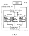
- FIG. 4 shows a structure of each memory control section.
- the address input to the memory is generated respectively in a write address generating section 18, a read address generating section 19, and a coding address generating section 20.
- the address signals output from each address generating section are in the time-division-multiplexed at an address selection section 21 and are input to the address terminal of the memory.
- Memory bank control section 22 manages the correspondence of the generated address signal and the memory bank which supplies it, and supplies the time division switching signal of the address signal to the address selection section 21 and a bank switching signal to the memory 2 or 13.
- the generation timing of each address generating section is controlled, also, by the memory bank control section 22.
- Each memory is divided into the plurality of banks capable of storing one error correction block and the interleave processing and the deinterleave processing are performed by switching this bank.
- the recording memory address control section 16 and the reproducing address control section 17 are in the same structure but the method of generating each address and the method of controlling a memory bank are different. Also, the deinterleave processing corresponds to the inversion of the interleave processing.
- FIG. 5 shows an example of the error correction code which is coded by the error correction encoder 3.
- the input data is treated in the sector of the 2048-byte unit, and the data block of 2064 bytes is constituted by adding information of 16 bytes to each sector.
- 2064-byte data is arranged in a form of 172 rows and 12 lines, to constitute a block of the 172 rows and 192 lines by arranging sixteen block of the 2064-byte data in the vertical direction.
- a Reed-Solomon product code is generated for the data block constituted in this method.
- external code is coded in the column direction.
- the coding of RS(208, 192, 17) code for each column data of 192 bytes is performed and a 16-byte parity is generated as an outer code parity.
- the internal code is coded in a row direction.
- the coding of RS(182, 172, 11) code for each row data of 172 bytes is performed and a 10-byte parity is generated as an inner code parity.
- a error correction block with the 182 rows and 208 lines is finally generated.
- sixteen sector blocks each with the 182 rows and 13 lines constitutes a data format.
- the error correction code is not limited to the code shown in FIG. 5 and may be coded with at least two error correction codes for the data arranged in similar blocks.
- the Reed-Solomon product code is one of the codes which are excellent for the error correction ability. Especially, there is a feature in which the error correction ability is high to the error continuously occurred (burst error). For example, in this format, if the data is taken out from the block shown in FIG. 6 one-by-one line, and is recorded in order, even if the data continuing sixteen rows in the maximum is lost by the error, it is possible to correct to the original data by the error correction processing.
- the burst error occurs with the influence of the defect of the optical disk which is a medium, the garbage and the dirt which adhered to the surface thereof and so on.
- the burst error which is occurred by these factors is not so large.
- it becomes necessary to improve the burst error correction ability because the defect and the garbage with the same size cause the larger burst error when the recording density becomes high.
- One method for improving the burst error correction ability of the Reed-Solomon product code is to increase the number of the outer code parities.
- the storage capacity in the whole optical disk is lowered because of lowering the rate of the input data occupied to the recorded data when increasing the outer code parity. Therefore, the interleave processing that the burst error correction ability can be improved without lowering the storage capacity.
- the interleave processing is a processing data in one error correction block are dispersed in a wide range by rearranging and multiplexing the data using a plurality of error correction blocks as a set.
- the burst error correction ability is improved proportional to the number of the error correction blocks in the set.
- FIG. 7 shows a processing procedure in case of performing an interleave in four blocks.
- the sector number of the ascending order by the sector unit is added to the input data in input order.
- the input data is assigned to four channels from A to D in the sector unit.
- the data of sixteen sectors of sector number from 100 to 115 are assigned to the channel A and assigned channels of the following data are switched in order of B, C, D, A for every sixteen sectors.
- a method of assigning to the channel is not limited to this example.
- a sector number 100 is assigned to the channel A and thereafter assigned channel may be switched for every one sector in order of C, D, A, B.
- the error correction coding is performed according to the error correction code shown in FIG. 5 by the sixteen sector unit every channel.
- the data of each channel is read sequentially after performing an error correction coding.
- the delay according to the channel is added to the read data and an offset is given to the output timing of the data.
- the offset between the channels is that the integer times of which the read time of the data for one correction block is divided, for example, by the number of the channels.
- the offset is set as the period corresponding to the four sectors which corresponds to the quarter of sixteen sectors.
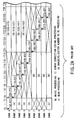
- FIG. 8 shows the timing after end of offset.
- Data multiplexing is performed among channels by setting total four sectors of one sector of each channel arranged in the horizontal direction as a unit by the data with the form shown in FIG. 8. For example, the data is read with being rearranged among total four sectors of sector numbers 112, 124, 136, 148 and is output.
- a multiplexing processing is often performed by the one-byte unit and the one row unit in the error correction block.
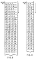
- FIG. 9 shows a data series after interleave processing when being rearranged by the one row unit.
- FIG. 10 and FIG. 11 show data series after the offset and the interleave when the interleave is performed in two blocks in the same method respectively.
- the offset between the channels becomes with the period corresponding to eight sectors. It does the multiplexing of the data during two channels arranged in the horizontal direction like the case of the four sector interleave. For example, rearrangement is performed in sector numbers 112 and 120.
- FIG. 7 for the explanation of the interleave processing, an error correction encoder and a sector delay section are provided for each channel, but these sequential processings can be realized by the memory and one error correction encoder as shown in FIG. 3.
- FIG. 12 shows an example of the interleave processing to the recording memory when the interleave is performed in four blocks.
- Each bank has a capacity which can store one error correction block and is divided into the subbanks with the capacity of the quarter thereof respectively.
- the input data is written into the memory with changing a bank in order every sixteen sectors.
- Writing to the bank A in order from the data with sector number 100 at period T0 is started.
- the writing data is written to the four subbanks every four sectors in the order.
- the error correction coding processing is started to the data sector numbers from 100 to 115 written into the bank A from period T4.
- a bank of the writing of the input data is switched to the bank B.
- the error correction coding processing of bank A is switched to the bank B from period T8 and the writing bank of the input data is switched to the bank C.
- read of the data in which an error correction coding is performed is started from the memory with performing the interleave.
- the data is read in parallel from the other three banks in addition to the bank A where coding has been completed in the past and is maintained by the memory. Since the error correction coding processing of bank B is completes in period T11, a reading from bank B is started from period T12. As a result, the offset corresponding to the four sectors occurs at the read starting timing for every banks.
- the writing of the input data to the bank A needs a periods from T0 to T3, but the reading of the output data, as a result of the interleave, requires four times of periods from period T8 to T23.
- the new data can not be written into each bank until the output of the data is completed. Therefore, new input data can be written into the bank A at period T24 or later.
- the number of the banks which is necessary for the interleave processing of four blocks becomes equal to or more than six.
- write processing is performed at one bank
- an error correction coding is performed at one bank
- read processing is performed at four banks at the same time. It finds that the bank which is not processing does not exist and that a memory is efficiently used.
- FIG. 13 shows an example when the interleave is performed in two blocks in the same method.
- the writing of the data with sector number 100 to the memory is started from period T0.
- the error correction coding processing starts from period T4 and the data is read with performing the interleave in period T8. Since the interleave is performed in two blocks, the time required for reading becomes a half in case of the four block interleave. Therefore, it is possible to use for the writing of the input data again from period T16. As a result, the number of the banks which is necessary to performing the two block interleave processing is equal to or more than four.
- the offset between the channel reading the interleaved data is equal to the four block interleave in an absolute time conversion, but becomes a half in case of the four block interleaving when converting to the time which reads data from each bank and the amount of read data.
- the deinterleave processing can be realized by the memory and one error correction decoder as shown in FIG. 1.
- FIG. 14 shows an example of the deinterleave processing when reproducing the interleaved data for four blocks.
- Each bank has a capacity capable of storing one error correction block like the recording memory and each bank is divided into the subbank with the capacity of the quarter thereof respectively.
- the reproduced data is reproduced by the order shown in FIG. 9 by the interleave processing at recording. This data is restored to the data series in the order of the original sector number by the deinterleave processing.
- the reproducing of the data including the sector number 100 is started in period T0. Since the data is interleaved in four blocks, the data to be reproduced in period T0 is multiplexed by the data of three sectors which has been previously reproduced in addition to the data with sector number 100.
- the multiplexed data according to the interleave method is separated and is written into four banks for every sector. It supposes that data with sector number 100 is written into the bank A.
- the reproducing of the data including sector number 116 is started in period T4.
- the data of sector number 116 is written into the bank B.
- the reproducing of the data including sector number 132 is started in period T8.
- the data of sector number 132 is written into the bank C.
- the four-block interleaved data becomes the same as a case that the offset for each channel is given.
- the offset between the channels is an integer times of which the read time of the data for one correction block is divided, foe example, by the number of the channels.
- the offset is set as the period corresponding to the four sectors which corresponds to the quarter of sixteen sectors.
- the sixteen sector data of sector number from 100 to 115 constituting one error correction block are made up to the bank A at period T15. Therefore, the error correction decoding processing to the data of the A bank is started from period T16. In parallel with the error correction decoding processing of the bank A, the reproduced data is sequentially written from banks B to E.
- the error correction decoding processing by bank A When the error correction decoding processing by bank A is completed, the error correction decoding processing is switched from the bank A to the bank B at period T20.
- the writing of the data to be is switched to the four banks of from the bank C to the bank F.
- the error corrected data of the bank A is read in order of the sector number and is output. Since the error correction decoding processing of the bank B is completed at period T23, the reading of the data is switched to the bank B at period T24.
- the writing of reproduced data to the bank A needs periods from period T0 to T15, but the reading can be performed a quarter period from T20 to T23 thereof since the reading can be executes at four times in speed thereof.
- the error correction decoding processing of the bank A is started at period T16 or later, since the error correction decoding processing can not be started when the writing of the data constituting one error correction block is not completed. Therefore, the new data to be reproduced can be written into the bank A becomes at period T24 or later. As a result, the number of the banks which is necessary for the four blocks deinterleave processing becomes equal to or more than six.
- the writing processing is performed at four banks, the error correction processing is performed at one bank, and the read processing is performed at one bank at the same time. It finds that the bank which is not processing does not exist and that a memory is efficiently used.
- FIG. 15 shows an example of the deinterleave processing when reproducing the interleaved data for tow blocks.
- the writing of the data with sector number 100 to the memory is started from period T0. Since two block deinterleave are performed, the writing of the data sector number from 100 to 115 constituting an error correction block becomes a half in case of the four block interleave. Therefore, the error correction decoding processing of the bank A is started from period T8. The reading of the output data is started from period T12 and is ended at period T15. Therefore, the bank A can be used for the writing of the data to be reproduced again from period T16. As a result, the number of the banks which is necessary for the deinterleave processing to the two-block interleaved data becomes equal to or more than four.
- the memory which is necessary for the interleave and the deinterleave processing can be reduced by adding an offset between the channels to be interleaved.
Landscapes
- Physics & Mathematics (AREA)
- Probability & Statistics with Applications (AREA)
- Engineering & Computer Science (AREA)
- Theoretical Computer Science (AREA)
- Error Detection And Correction (AREA)
- Signal Processing For Digital Recording And Reproducing (AREA)
Applications Claiming Priority (3)
| Application Number | Priority Date | Filing Date | Title |
|---|---|---|---|
| JP9267048A JPH11110920A (ja) | 1997-09-30 | 1997-09-30 | 誤り訂正符号化方法及び装置、誤り訂正復号化方法及び装置、並びにデータ記録・再生装置、並びに記憶媒体 |
| JP267048/97 | 1997-09-30 | ||
| JP26704897 | 1997-09-30 |
Publications (3)
| Publication Number | Publication Date |
|---|---|
| EP0907257A2 true EP0907257A2 (de) | 1999-04-07 |
| EP0907257A3 EP0907257A3 (de) | 2000-04-12 |
| EP0907257B1 EP0907257B1 (de) | 2001-12-05 |
Family
ID=17439325
Family Applications (1)
| Application Number | Title | Priority Date | Filing Date |
|---|---|---|---|
| EP98118429A Expired - Lifetime EP0907257B1 (de) | 1997-09-30 | 1998-09-29 | Fehlerkorrektur verschachtelter Datenblöcke |
Country Status (7)
| Country | Link |
|---|---|
| US (1) | US6216245B1 (de) |
| EP (1) | EP0907257B1 (de) |
| JP (1) | JPH11110920A (de) |
| KR (1) | KR100285127B1 (de) |
| CN (1) | CN1254922C (de) |
| DE (1) | DE69802770T2 (de) |
| TW (1) | TW408306B (de) |
Cited By (1)
| Publication number | Priority date | Publication date | Assignee | Title |
|---|---|---|---|---|
| US11757472B1 (en) | 2022-05-16 | 2023-09-12 | Seagate Technology Llc | Coarse interleaving |
Families Citing this family (23)
| Publication number | Priority date | Publication date | Assignee | Title |
|---|---|---|---|---|
| KR100354744B1 (ko) * | 1998-08-04 | 2002-12-11 | 삼성전자 주식회사 | 고밀도기록매체를위한인터리브방법및그회로 |
| US6581178B1 (en) * | 1999-02-15 | 2003-06-17 | Nec Corporation | Error correction coding/decoding method and apparatus |
| JP2000251419A (ja) * | 1999-02-26 | 2000-09-14 | Sony Corp | 読み出し制御装置、再生装置、記録装置およびその方法 |
| KR100312347B1 (ko) * | 1999-08-26 | 2001-11-03 | 정주호 | 자동차의 배기가스 정화용 촉매 컨버터 조절장치 |
| JP3459609B2 (ja) * | 2000-03-17 | 2003-10-20 | 三洋電機株式会社 | ライトキャッシュ回路、ライトキャッシュ回路を備えた記録装置、およびライトキャッシュ方法 |
| JP4130534B2 (ja) * | 2001-02-07 | 2008-08-06 | 株式会社東芝 | 情報記録媒体、情報記録装置、情報記録方法、情報再生装置、及び情報再生方法 |
| US20020157057A1 (en) * | 2001-04-20 | 2002-10-24 | Samsung Electronics Co., Ltd. | Optical information recording medium and data recording apparatus thereon |
| US7159165B2 (en) * | 2001-04-20 | 2007-01-02 | Samsung Electronics Co., Ltd. | Optical recording medium, data recording or reproducing apparatus and data recording or reproducing method used by the data recording or reproducing apparatus |
| US6910174B2 (en) | 2001-06-01 | 2005-06-21 | Dphi Acquisitions, Inc. | Error correction code block format |
| US7117421B1 (en) * | 2002-05-31 | 2006-10-03 | Nvidia Corporation | Transparent error correction code memory system and method |
| US20040015771A1 (en) * | 2002-07-16 | 2004-01-22 | Menahem Lasser | Error correction for non-volatile memory |
| US8386797B1 (en) * | 2002-08-07 | 2013-02-26 | Nvidia Corporation | System and method for transparent disk encryption |
| US7178088B2 (en) * | 2002-11-18 | 2007-02-13 | Matsushita Electric Industrial Co., Ltd. | Method and circuit for error correction, error correction encoding, data reproduction, or data recording |
| US7386754B2 (en) * | 2003-10-16 | 2008-06-10 | Seagate Technology Llc | Method and apparatus to improve magnetic disc drive reliability using excess un-utilized capacity |
| US7418644B2 (en) * | 2004-03-01 | 2008-08-26 | Hewlett-Packard Development Company, L.P. | System for error correction coding and decoding |
| TWI259443B (en) * | 2005-03-11 | 2006-08-01 | Lite On It Corp | Dynamic speed control method for storage device |
| US7430701B2 (en) * | 2005-06-16 | 2008-09-30 | Mediatek Incorporation | Methods and systems for generating error correction codes |
| ATE517372T1 (de) * | 2007-01-24 | 2011-08-15 | Oce Tech Bv | Bilderzeugungsvorrichtung mit funktion zum zählen der von der vorrichtung angezeigten bilder |
| CN101483443B (zh) * | 2008-12-26 | 2012-07-25 | 中国航空无线电电子研究所 | Turbo乘积码优化编译码算法的FPGA实现方法 |
| JP2009110659A (ja) * | 2009-01-23 | 2009-05-21 | Victor Co Of Japan Ltd | 情報記録媒体、情報記録媒体再生装置、情報記録媒体再生方法、情報記録媒体記録装置、情報記録媒体記録方法 |
| JP2009104785A (ja) * | 2009-02-16 | 2009-05-14 | Victor Co Of Japan Ltd | 情報記録媒体、情報記録媒体再生装置、情報記録媒体再生方法、情報記録媒体記録装置、情報記録媒体記録方法 |
| KR101607307B1 (ko) * | 2009-07-09 | 2016-03-30 | 삼성전자주식회사 | 정보 부호화 방법, 정보 복호화 방법, 기록/재생 장치 및 정보 저장 매체 |
| WO2022139849A1 (en) | 2020-12-26 | 2022-06-30 | Intel Corporation | Adaptive error correction to improve for system memory reliability, availability, and serviceability (ras) |
Family Cites Families (10)
| Publication number | Priority date | Publication date | Assignee | Title |
|---|---|---|---|---|
| JP2526875B2 (ja) * | 1986-11-05 | 1996-08-21 | ソニー株式会社 | デイジタル情報記録装置 |
| JP2786291B2 (ja) * | 1990-01-09 | 1998-08-13 | 松下電器産業株式会社 | デジタル信号記録方法およびデジタル信号記録再生装置 |
| US5483541A (en) * | 1993-09-13 | 1996-01-09 | Trw Inc. | Permuted interleaver |
| BR9505853A (pt) * | 1994-03-01 | 1996-02-21 | Sony Corp | Processo e aparelho de codificação e de decodificação de sinal digital e meio de registro de sinal digital |
| JP2882302B2 (ja) * | 1995-02-24 | 1999-04-12 | 株式会社日立製作所 | 情報の記録方法及び再生方法 |
| MY116522A (en) * | 1995-05-31 | 2004-02-28 | Sony Corp | Data recording/reproducing apparatus, method thereof, and data recording medium |
| JP4209953B2 (ja) | 1995-05-31 | 2009-01-14 | ソニー株式会社 | データ記録/再生装置および方法、並びにディスク状記録媒体 |
| US5898710A (en) * | 1995-06-06 | 1999-04-27 | Globespan Technologies, Inc. | Implied interleaving, a family of systematic interleavers and deinterleavers |
| US5724917A (en) * | 1996-06-21 | 1998-03-10 | Milliken Research Corporation | Cattle mattress |
| JP3956417B2 (ja) * | 1997-02-28 | 2007-08-08 | ソニー株式会社 | ディスク装置及びディスク再生方法 |
-
1997
- 1997-09-30 JP JP9267048A patent/JPH11110920A/ja active Pending
-
1998
- 1998-09-29 EP EP98118429A patent/EP0907257B1/de not_active Expired - Lifetime
- 1998-09-29 TW TW087116195A patent/TW408306B/zh not_active IP Right Cessation
- 1998-09-29 DE DE69802770T patent/DE69802770T2/de not_active Expired - Fee Related
- 1998-09-30 CN CNB98124520XA patent/CN1254922C/zh not_active Expired - Fee Related
- 1998-09-30 US US09/163,205 patent/US6216245B1/en not_active Expired - Fee Related
- 1998-09-30 KR KR1019980041930A patent/KR100285127B1/ko not_active Expired - Fee Related
Cited By (1)
| Publication number | Priority date | Publication date | Assignee | Title |
|---|---|---|---|---|
| US11757472B1 (en) | 2022-05-16 | 2023-09-12 | Seagate Technology Llc | Coarse interleaving |
Also Published As
| Publication number | Publication date |
|---|---|
| EP0907257B1 (de) | 2001-12-05 |
| EP0907257A3 (de) | 2000-04-12 |
| DE69802770D1 (de) | 2002-01-17 |
| JPH11110920A (ja) | 1999-04-23 |
| CN1254922C (zh) | 2006-05-03 |
| US6216245B1 (en) | 2001-04-10 |
| CN1217534A (zh) | 1999-05-26 |
| TW408306B (en) | 2000-10-11 |
| KR100285127B1 (ko) | 2001-03-15 |
| DE69802770T2 (de) | 2002-07-18 |
| KR19990030340A (ko) | 1999-04-26 |
Similar Documents
| Publication | Publication Date | Title |
|---|---|---|
| EP0907257B1 (de) | Fehlerkorrektur verschachtelter Datenblöcke | |
| KR950003638B1 (ko) | 에러 검출/정정 코드 디코딩 장치 | |
| US5151905A (en) | Data recording method | |
| US7984340B2 (en) | Method of recording/reproducing digital data and apparatus for same | |
| US4751590A (en) | Recording audio signals | |
| KR900003595B1 (ko) | Pcm 신호를 기록하기 위한 방법 및 장치 | |
| CN1975911B (zh) | 用于处理光盘数据的装置和方法 | |
| JPH11297000A (ja) | データ生成方法及びデータ生成装置 | |
| JP3592597B2 (ja) | エラー訂正装置及びプログラム記録媒体 | |
| JPS6338897B2 (de) | ||
| JPH0783275B2 (ja) | エラ−訂正符号の復号装置 | |
| JPS59198513A (ja) | デイジタル信号処理装置 | |
| KR100266165B1 (ko) | 에러정정코드 처리를 위한 디램 억세스 방법(Method of Accessing DRAM for Processing Error Correction Code) | |
| JPH08125548A (ja) | 誤り訂正符号化回路、誤り訂正復号化回路、誤り訂正符号化・復号化回路、および、それを用いたディジタル装置 | |
| KR100665442B1 (ko) | 에러정정용 메모리 제어장치 및 방법 | |
| JPS61271671A (ja) | 再生ビデオデータの処理装置 | |
| JPH0473334B2 (de) | ||
| JP2001168737A (ja) | データ記録装置およびデータ再生装置 | |
| JPH0785338B2 (ja) | 回転ヘッド形磁気記録装置及びこれに用いる信号処理回路 |
Legal Events
| Date | Code | Title | Description |
|---|---|---|---|
| PUAI | Public reference made under article 153(3) epc to a published international application that has entered the european phase |
Free format text: ORIGINAL CODE: 0009012 |
|
| 17P | Request for examination filed |
Effective date: 19981026 |
|
| AK | Designated contracting states |
Kind code of ref document: A2 Designated state(s): DE FR GB NL |
|
| AX | Request for extension of the european patent |
Free format text: AL;LT;LV;MK;RO;SI |
|
| PUAL | Search report despatched |
Free format text: ORIGINAL CODE: 0009013 |
|
| AK | Designated contracting states |
Kind code of ref document: A3 Designated state(s): AT BE CH CY DE DK ES FI FR GB GR IE IT LI LU MC NL PT SE |
|
| AX | Request for extension of the european patent |
Free format text: AL;LT;LV;MK;RO;SI |
|
| RIC1 | Information provided on ipc code assigned before grant |
Free format text: 7H 03M 13/27 A, 7H 03M 13/29 B |
|
| 17Q | First examination report despatched |
Effective date: 20001010 |
|
| AKX | Designation fees paid |
Free format text: DE FR GB NL |
|
| GRAG | Despatch of communication of intention to grant |
Free format text: ORIGINAL CODE: EPIDOS AGRA |
|
| GRAG | Despatch of communication of intention to grant |
Free format text: ORIGINAL CODE: EPIDOS AGRA |
|
| GRAH | Despatch of communication of intention to grant a patent |
Free format text: ORIGINAL CODE: EPIDOS IGRA |
|
| GRAH | Despatch of communication of intention to grant a patent |
Free format text: ORIGINAL CODE: EPIDOS IGRA |
|
| GRAA | (expected) grant |
Free format text: ORIGINAL CODE: 0009210 |
|
| AK | Designated contracting states |
Kind code of ref document: B1 Designated state(s): DE FR GB NL |
|
| PG25 | Lapsed in a contracting state [announced via postgrant information from national office to epo] |
Ref country code: NL Free format text: LAPSE BECAUSE OF FAILURE TO SUBMIT A TRANSLATION OF THE DESCRIPTION OR TO PAY THE FEE WITHIN THE PRESCRIBED TIME-LIMIT Effective date: 20011205 |
|
| REG | Reference to a national code |
Ref country code: GB Ref legal event code: IF02 |
|
| REF | Corresponds to: |
Ref document number: 69802770 Country of ref document: DE Date of ref document: 20020117 |
|
| NLV1 | Nl: lapsed or annulled due to failure to fulfill the requirements of art. 29p and 29m of the patents act | ||
| ET | Fr: translation filed | ||
| PGFP | Annual fee paid to national office [announced via postgrant information from national office to epo] |
Ref country code: FR Payment date: 20020910 Year of fee payment: 5 |
|
| PGFP | Annual fee paid to national office [announced via postgrant information from national office to epo] |
Ref country code: GB Payment date: 20020925 Year of fee payment: 5 |
|
| PGFP | Annual fee paid to national office [announced via postgrant information from national office to epo] |
Ref country code: DE Payment date: 20021002 Year of fee payment: 5 |
|
| PLBE | No opposition filed within time limit |
Free format text: ORIGINAL CODE: 0009261 |
|
| STAA | Information on the status of an ep patent application or granted ep patent |
Free format text: STATUS: NO OPPOSITION FILED WITHIN TIME LIMIT |
|
| 26N | No opposition filed | ||
| PG25 | Lapsed in a contracting state [announced via postgrant information from national office to epo] |
Ref country code: GB Free format text: LAPSE BECAUSE OF NON-PAYMENT OF DUE FEES Effective date: 20030929 |
|
| PG25 | Lapsed in a contracting state [announced via postgrant information from national office to epo] |
Ref country code: DE Free format text: LAPSE BECAUSE OF NON-PAYMENT OF DUE FEES Effective date: 20040401 |
|
| GBPC | Gb: european patent ceased through non-payment of renewal fee |
Effective date: 20030929 |
|
| PG25 | Lapsed in a contracting state [announced via postgrant information from national office to epo] |
Ref country code: FR Free format text: LAPSE BECAUSE OF NON-PAYMENT OF DUE FEES Effective date: 20040528 |
|
| REG | Reference to a national code |
Ref country code: FR Ref legal event code: ST |