EP0908828B1 - Verteiltes Speicherzugriffsteuersystem und Verfahren - Google Patents
Verteiltes Speicherzugriffsteuersystem und Verfahren Download PDFInfo
- Publication number
- EP0908828B1 EP0908828B1 EP98402449A EP98402449A EP0908828B1 EP 0908828 B1 EP0908828 B1 EP 0908828B1 EP 98402449 A EP98402449 A EP 98402449A EP 98402449 A EP98402449 A EP 98402449A EP 0908828 B1 EP0908828 B1 EP 0908828B1
- Authority
- EP
- European Patent Office
- Prior art keywords
- memory
- entities
- entity
- allocated
- signal
- Prior art date
- Legal status (The legal status is an assumption and is not a legal conclusion. Google has not performed a legal analysis and makes no representation as to the accuracy of the status listed.)
- Expired - Lifetime
Links
Images
Classifications
-
- G—PHYSICS
- G06—COMPUTING OR CALCULATING; COUNTING
- G06F—ELECTRIC DIGITAL DATA PROCESSING
- G06F13/00—Interconnection of, or transfer of information or other signals between, memories, input/output devices or central processing units
- G06F13/14—Handling requests for interconnection or transfer
- G06F13/16—Handling requests for interconnection or transfer for access to memory bus
- G06F13/18—Handling requests for interconnection or transfer for access to memory bus based on priority control
Definitions
- the invention relates to shared access control to a random access memory by several entities that can operate completely asynchronously.
- the invention applies advantageously but not exclusively to the field of television. Indeed, in such an application, the data displayed on the TV screen is delivered by a screen controller after reading a random access memory whose content is the result of a software processing performed by a microprocessor.
- clock signals respectively clocking the screen controller and the microprocessor are totally asynchronous in frequency and phase and each of these two entities may be likely to want to access the memory at one time.
- the aim of the invention is to provide a radically different solution to access control shared to the same memory.
- the invention proposes the use of a simple random access memory, the sharing of which is not physical by different accesses. (as in dual access memories) but temporal. More specifically, time sharing of memory access requests is performed, and shared memory accesses are managed by a sequencer which will segment the time into access windows specifically reserved for each of the user entities of the memory. memory. The sequencer is punctuated by a clock chosen according to the priorities of the different entities. The internal clock signal of the highest priority entity will be the one that will rhythm the sequencer. Finally, a non-priority entity, or auxiliary, will, with each access request, wait for its next access window to read or store the data being processed.
- the invention proposes a shared access control method to a random access memory, in which a plurality of peripheral entities clocked respectively by their own internal clock signal, are able to access said memory. memory.
- the random access memory is a single access memory, that is to say a single access memory, and a priority entity is defined among the set of peripheral entities, the other entities being defined as being auxiliary entities.
- a repetitive time frame is generated, paced by the internal clock signal of the priority entity, this frame being subdivided into time windows forming several groups of windows respectively allocated to the peripheral entities. And each peripheral entity is allowed to access said memory only during the windows allocated to it.
- the priority entity will advantageously be the screen controller.
- auxiliary peripheral entities may be simple data samplers.
- Other auxiliary entities may comprise a central microprocessor unit and input / output means connected to said memory and able to contain data to be written in the memory or data extracted from the memory and to be read by the user. central unit.
- the data present in the input / output means is validated during the next time slot allocated to said central unit and the internal operation of the central unit is frozen until said validation.
- the invention also relates to an access control system shared with a random access memory.
- the system according to the invention further comprises a control interface comprising a sequencer clocked by the internal clock signal of the priority entity, so as to develop a repetitive temporal frame divided into time windows forming several groups of windows respectively allocated to peripheral entities.
- the interface also comprises control means capable of responding to an access request signal emanating from a peripheral entity, to deliver to the input / output means of this entity the data validation signal only in the course of a window allocated to this entity, thus allowing the access of this entity to the memory.
- control means advantageously comprise suitable means of inhibition, in the presence of a memory access request signal transmitted by the central unit to the central unit. during a time window that is not allocated to it, to freeze the operation internal of the central unit until the reception of the data validation signal.
- This "freezing" or this inhibition of the operation of the central unit may result in a total interruption of the operation of the central unit or in a freeze or a freezing of the contents of the internal registers or latches so that it There is no further evolution of the data delivered by these flip-flops until the gel signal is deactivated.
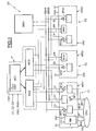
- the reference SY generally designates a system according to the invention, making it possible here to control the accesses of three peripheral entities, or more simply peripheral devices, P1, P2 and P3, to an MMV random access memory.
- peripheral P1 comprises in the example described, a microprocessor CPU central unit as well as input / output means MES1 connected to the address bus BSR1 of the memory and on the BSR2 data bus of this memory.
- these input / output means MES1 comprise an output port BF10, connected to the address bus BSR1, comprising a buffer memory, connected to the address bus BS10 of the central unit for storing an address.
- This output port BF10 is conventionally controlled by an address validation signal E1 for validating and effectively delivering the address on the address bus BSR1 of the memory.
- the input / output means MES 1 comprise a data input port BF11 comprising a buffer memory, connected between the data bus B SR2 of the memory MV and the data bus BS11 of the central unit. This input port is controlled by a signal LD1 for validating the data extracted from the memory MMV.
- the means MES 1 comprise a data output port BF12 controlled by a data validation signal D1 for actually writing the data in the memory MMV.
- MES 1 of course comprise a control port for the exchange of the different validation signals E1, LD1, D1, but also to deliver a signal C1 of access request to the memory and a signal RW1 representative of the reading direction. writing.
- the second peripheral P2 which is, for example, in a television application, the screen controller, comprises input / output means MES2 comprising a control port and an output port BF20 connected to the address bus BSR1.
- memory comprising in particular an address pointer and controllable by an address validation signal E2.
- these input / output means MES2 here comprise only a data input port BF21 comprising a buffer memory, connected to the data bus BSR2 of the memory and controllable by a data validation signal LD2.
- the system according to the invention also includes an IF interface for controlling and managing access to the MMV memory.
- this IF interface comprises processing means that can be implemented at least partially in a software manner within a microcontroller for example, or by a specific integrated circuit (ASIC), or simply by simple hardware integration (“ hardware ”) in the system (integrated circuit for example).
- ASIC application specific integrated circuit
- hardware simple hardware integration
- the IF interface has been functionally broken down.
- a main controller MC1 comprising in particular a sequencer SQ clocked by the clock signal of one of the devices so as to develop a repetitive time frame which will be discussed in more detail below on the structure, and a bus controller MC2 data delivering the data enable signals LDi and / or Di and an address bus controller MC3 delivering the address validation signals Ei.
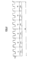
- the development of the repetitive time frame TR depends on the priority character of one of the peripherals. More precisely, one of the peripheral entities P1, P2, P3 is selected, the one whose real-time processing is the highest priority, that is to say for example the one with the most real-time constraints.
- the priority real-time processing is that managing the display screen so as not to deteriorate the quality and stability of the displayed image. It is therefore the peripheral entity P2 corresponding to the screen controller, which will be designated as the priority entity, the other entities being the auxiliary entities.
- the duration of the TR frame will be chosen here as being the time required to display a character on the screen.
- This frame duration TR corresponds to a certain number of periods of the clock signal CK2 of the screen controller. This number of clock periods is typically 18, but for simplification purposes, only 12 are shown in FIG.
- the remaining access windows namely the windows S1, S3 and S5 are reserved for the other peripheral entities.
- the CPU S1 and S5 are allocated to the CPU, while the S3 device is allocated to the peripheral entity P3.
- the sequencer of the control interface is clocked by the clock signal CK2 of the priority entity.
- requests C2 successive accesses issued by the P2 device will be synchronous with the occurrence of time windows S2, S4 and S6.
- the address validation signals E2 and LD2 will therefore be delivered by the control means MC2 and MC3 during these time slots also allowing access of the device P2 to the memory MMV.
- the control interface will deliver the address validation signal E3 and the data validation signal D3 or LD3 according to the logical value of a signal RW3, only during the next access window which is allocated to the device P3, in this case the window S3.
- the device P3 will actually have access to the memory MMV during the window S3 allocated to it.
- the same principle is applied to the device P1 in the case where an access request signal C1, associated with a write or read request signal RW1, is emitted by the device P1 during a time window of access that is not allocated to him.
- it is furthermore necessary to freeze the internal operation of the central processing unit CPU until the reception of the validation signal LD1 or D1 as a function of the reading or writing direction.
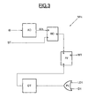
- the IF control interface comprises MH inhibiting means which is shown here for simplification purposes within the MES1 block.
- these MH inhibiting means comprise an address decoder AD receiving the address sent on the bus BS10 of the central unit and intended to verify that this address corresponds to an effective address. of memory. If this is the case, the output SEL signal of the decoder goes to logic level "1" and is stored in a flip-flop referenced BD controlled by the address validation signal ST delivered by the central unit.
- this address enable signal ST goes to 1
- the output of the flip-flop BD which is connected to the input of an FF flip flop (flip flop) passes the output of this flip-flop FF to 1.
- the signal corresponding logic WT which is delivered to the CPU CPU, then acts as a freeze signal of that unit Central. It should also be noted that the transition of the signal WT from the logical state "0" to the logic state "1" can be used as a condition for generating the access request signal C1.
- the MH inhibiting means also comprise a DT transitions detector whose output is connected to the reset input R of the FF output flip-flop, and the input of which is connected to the output of a logic gate. OR, referenced PL, and receiving as input the validation signals LD1 and D1.
- the transmission by the controller MC2 of the control interface of the data validation signal LD1 or D1 results in a rising transition of the corresponding signal.
- the detection of this transition by the detector DT has the effect of returning the output of the flip-flop FF to zero, that is to say, to redimit the WT gel signal to a low state, which has the consequence of reactivate the internal operation of the CPU.
Landscapes
- Engineering & Computer Science (AREA)
- Theoretical Computer Science (AREA)
- Physics & Mathematics (AREA)
- General Engineering & Computer Science (AREA)
- General Physics & Mathematics (AREA)
- Multi Processors (AREA)
- Memory System (AREA)
Claims (4)
- Verfahren zur Steuerung der verteilten Zugriffe auf einen Arbeitsspeicher, einem Verfahren, in welchem mehrere Peripherieeinheiten, die jeweils mit ihrem eigenen internen Taktsignal getaktet werden, auf den Speicher zugreifen können, dadurch gekennzeichnet, daß
aus der Gesamtheit der Peripherieeinheiten eine vorrangige Einheit (P2) definiert wird und die anderen Einheiten (P1,P3) als nachrangige Einheiten definiert werden, wobei der Speicher (MMV) ein Speicher mit einfachem Zugriff ist,
ein sich wiederholender Zeitrahmen (TR) ausgearbeitet wird, der von dem internen Taktsignal (CK2) der vorrangigen Einheit getaktet wird und in Zeitfenster (S1-S6) unterteilt ist, die mehrere Fenstergruppen bilden, die jeweils den Peripherieeinheiten zugewiesen sind, und
jeder Peripherieeinheit erlaubt wird, nur während der Fenster, die ihr zugewiesen sind, auf den Speicher zuzugreifen. - Verfahren nach Anspruch 1, in welchem eine (P1) der nachrangigen Einheiten eine Zentraleinheit (CPV) eines Mikroprozessors und mit dem Speicher verbundene Eingabe/Ausgabe-Einrichtungen (MES1) aufweist, die in den Speicher zu schreibende Daten oder aus dem Speicher zu holende und von der Zentraleinheit zu lesende Daten halten können, dadurch gekennzeichnet, daß
bei Anwesenheit eines Speicherzugriff-Anforderungssignals (C1), das von der Zentraleinheit während eines ihm nicht zugewiesenen Zeitfensters ausgesandt worden ist, die in den Eingabe/Ausgabe-Einrichtungen vorhandenen Daten während des nächsten, der Zentraleinheit zugewiesenen Zeitfensters freigegeben werden und der interne Betriebsablauf der Zentraleinheit bis zur dieser Freigabe eingefroren wird. - System zur Steuerung der verteilten Zugriffe auf einen Arbeitsspeicher, dadurch gekennzeichnet, daß es aufweist:einen Areitsspeicher mit einfachem Zugriff (MMV), der mit einem Datenbus und einem Adreßbus verbunden ist,mehrere Peripherieeinheiten (P1-P3), die in eine vorrangige Einheit und in nachrangige Einheiten eingeteilt sind, jeweils von ihrem eigenen internen Taktsignal getaktet werden, jeweils ein Speicherzugriff-Anforderungssignal ausgeben können und jeweils mit dem Datenbus und dem Adreßbus verbundene Eingabe/Ausgabe-Einrichtungen aufweisen, die Speichereinrichtungen aufweisen, die aus dem Speicher geholte Daten oder in den Speicher zu schreibende Daten halten können, und einen Steueranschluß aufweisen, um mindestens ein Freigabesignal zur Freigabe der in den Eingabe/Ausgabe-Einrichtungen gehaltenen Daten zu empfangen, undeine Schnittstelle (IF), die aufweist:eine Ablaufsteuerung (SQ), die von dem internen Taktsignal der vorrangigen Einheit getaktet wird, um einen sich wiederholenden Zeitrahmen auszuarbeiten, der in Zeitfenster unterteilt ist, die mehrere Fenstergruppen bilden, die jeweils den Peripherieeinheiten zugewiesen sind, undSteuereinrichtungen (MC1-MC3), die in der Lage sind, als Antwort auf ein von einer Einheit herkommendes Zugriffsanforderungssignal das Datenfreigabesignal nur während eines Fensters, das dieser Einheit zugewiesen ist, zu den Eingabe/Ausgabe-Einrichtungen dieser Einheit auszugeben, um dadurch den Zugriff dieser Einheit auf den Speicher zu erlauben.
- System nach Anspruch 3, dadurch gekennzeichnet, daß eine (P1) der nachrangigen Einheiten eine Mikroprozessor-Zentraleinheit aufweist, dadurch, daß die Steuereinrichtungen Hemmeinrichtungen (MH) aufweisen, die in der Lage sind, bei Anwesenheit eines Speicherzugriff-Anforderungssignals, das von der Zentraleinheit während eines Zeitfensters, das ihm nicht zugewiesen ist, ausgesandt worden ist, den internen Betriebsablauf der Zentraleinheit bis zum Empfang des Datenfreigabesignals einzufrieren.
Applications Claiming Priority (2)
| Application Number | Priority Date | Filing Date | Title |
|---|---|---|---|
| FR9712631 | 1997-10-09 | ||
| FR9712631A FR2769727B1 (fr) | 1997-10-09 | 1997-10-09 | Procede et systeme de controle d'acces partages a une memoire vive |
Publications (2)
| Publication Number | Publication Date |
|---|---|
| EP0908828A1 EP0908828A1 (de) | 1999-04-14 |
| EP0908828B1 true EP0908828B1 (de) | 2007-01-03 |
Family
ID=9512035
Family Applications (1)
| Application Number | Title | Priority Date | Filing Date |
|---|---|---|---|
| EP98402449A Expired - Lifetime EP0908828B1 (de) | 1997-10-09 | 1998-10-06 | Verteiltes Speicherzugriffsteuersystem und Verfahren |
Country Status (5)
| Country | Link |
|---|---|
| US (1) | US6587932B2 (de) |
| EP (1) | EP0908828B1 (de) |
| JP (1) | JPH11175392A (de) |
| DE (1) | DE69836787D1 (de) |
| FR (1) | FR2769727B1 (de) |
Families Citing this family (5)
| Publication number | Priority date | Publication date | Assignee | Title |
|---|---|---|---|---|
| US7587530B2 (en) * | 2003-08-20 | 2009-09-08 | Hewlett-Packard Development Company, L.P. | Method and apparatus for managing device reservation |
| US20060041705A1 (en) * | 2004-08-20 | 2006-02-23 | International Business Machines Corporation | System and method for arbitration between shared peripheral core devices in system on chip architectures |
| JP5037814B2 (ja) * | 2005-11-30 | 2012-10-03 | キヤノン株式会社 | メモリ制御装置及びメモリ制御方法 |
| US20090013134A1 (en) * | 2007-07-06 | 2009-01-08 | Transcend Information , Inc. | Memory apparatus and protecting method thereof |
| JP2023526659A (ja) * | 2020-05-21 | 2023-06-22 | シェルタード ウィングス インコーポレイテッド | マルチロール型観察光学機器用レティクル |
Family Cites Families (25)
| Publication number | Priority date | Publication date | Assignee | Title |
|---|---|---|---|---|
| US4181933A (en) * | 1978-04-18 | 1980-01-01 | Mohawk Data Sciences Corp. | Memory access and sharing control system |
| FR2461300A1 (fr) | 1979-07-10 | 1981-01-30 | Lucas Industries Ltd | Appareil de calcul numerique comportant deux dispositifs de calcul numerique dont chacun est commande par sa propre horloge |
| US4313161A (en) * | 1979-11-13 | 1982-01-26 | International Business Machines Corporation | Shared storage for multiple processor systems |
| JPS5734263A (en) | 1980-08-04 | 1982-02-24 | Kokusai Electric Co Ltd | Simple multiprocessor system |
| JPS5858667A (ja) | 1981-10-02 | 1983-04-07 | Hitachi Ltd | メモリ共有方式 |
| DE3313840A1 (de) * | 1983-04-16 | 1984-10-18 | Standard Elektrik Lorenz Ag, 7000 Stuttgart | Nachrichtenuebertragungssystem mit vielfachzugriff im zeitmultiplex (tdma) mit dezentral synchronisiertem zugriff |
| US4709347A (en) * | 1984-12-17 | 1987-11-24 | Honeywell Inc. | Method and apparatus for synchronizing the timing subsystems of the physical modules of a local area network |
| JPS61282954A (ja) * | 1985-06-07 | 1986-12-13 | Hitachi Electronics Eng Co Ltd | アクセス制御方式 |
| JPH02135564A (ja) | 1988-11-16 | 1990-05-24 | Sony Corp | データ処理装置 |
| US5218680A (en) * | 1990-03-15 | 1993-06-08 | International Business Machines Corporation | Data link controller with autonomous in tandem pipeline circuit elements relative to network channels for transferring multitasking data in cyclically recurrent time slots |
| DE4008729A1 (de) * | 1990-03-19 | 1991-09-26 | Rheydt Kabelwerk Ag | Verfahren zum uebertragen von zeitdiskreten informationen |
| JPH0520253A (ja) | 1991-07-12 | 1993-01-29 | Matsushita Electric Ind Co Ltd | データ処理装置 |
| US5521925A (en) * | 1993-09-09 | 1996-05-28 | Hughes Aircraft Company | Method and apparatus for providing mixed voice and data communication in a time division multiple access radio communication system |
| US5602836A (en) * | 1993-11-24 | 1997-02-11 | Lucent Technologies Inc. | Multiple access cellular communication with circular interleaving and reduced dropped-packet runlengths |
| US5583856A (en) * | 1994-06-10 | 1996-12-10 | Harris Corporation | Integrated network switch with large capacity switch architecture using selectable interfaces between peripherals and switch memories |
| US5764893A (en) * | 1994-08-03 | 1998-06-09 | Matsushita Electrical Co. Ltd. | Video-on-demand system uses adjusting positions of slots in a slot table to address additional image data distribution request from terminal devices |
| US5586264A (en) * | 1994-09-08 | 1996-12-17 | Ibm Corporation | Video optimized media streamer with cache management |
| DE69433872T2 (de) * | 1994-10-26 | 2005-07-14 | International Business Machines Corp. | Mediumzugriffssteuerungsschema für drahtlose lokale Netze mit verschachtelten Zeitmultiplexrahmen variabler Länge |
| US5721815A (en) * | 1995-06-07 | 1998-02-24 | International Business Machines Corporation | Media-on-demand communication system and method employing direct access storage device |
| US5815662A (en) * | 1995-08-15 | 1998-09-29 | Ong; Lance | Predictive memory caching for media-on-demand systems |
| US5737747A (en) * | 1995-10-27 | 1998-04-07 | Emc Corporation | Prefetching to service multiple video streams from an integrated cached disk array |
| JPH1091360A (ja) * | 1996-09-12 | 1998-04-10 | Fujitsu Ltd | ディスク制御方式 |
| DE19651707A1 (de) * | 1996-12-12 | 1998-08-20 | Altvater Air Data Systems Gmbh | Verfahren zum Übertragen von Datenpaketen |
| US6141336A (en) * | 1996-12-13 | 2000-10-31 | International Business Machines Corporation | Traffic scheduling method, system and article of manufacture for a wireless access to an asynchronous transfer mode network |
| US6298370B1 (en) * | 1997-04-04 | 2001-10-02 | Texas Instruments Incorporated | Computer operating process allocating tasks between first and second processors at run time based upon current processor load |
-
1997
- 1997-10-09 FR FR9712631A patent/FR2769727B1/fr not_active Expired - Fee Related
-
1998
- 1998-09-30 JP JP10277424A patent/JPH11175392A/ja active Pending
- 1998-10-06 EP EP98402449A patent/EP0908828B1/de not_active Expired - Lifetime
- 1998-10-06 DE DE69836787T patent/DE69836787D1/de not_active Expired - Lifetime
- 1998-10-09 US US09/169,715 patent/US6587932B2/en not_active Expired - Lifetime
Also Published As
| Publication number | Publication date |
|---|---|
| JPH11175392A (ja) | 1999-07-02 |
| EP0908828A1 (de) | 1999-04-14 |
| DE69836787D1 (de) | 2007-02-15 |
| US20010042177A1 (en) | 2001-11-15 |
| US6587932B2 (en) | 2003-07-01 |
| FR2769727B1 (fr) | 2000-01-28 |
| FR2769727A1 (fr) | 1999-04-16 |
Similar Documents
| Publication | Publication Date | Title |
|---|---|---|
| EP0032863A1 (de) | Verfahren und Vorrichtung zum Steuern von Konflikten bei Mehrfachzugriffen zum selben CACHE-Speicher eines digitalen Datenverarbeitungssystems mit zumindest zwei, je einen CACHE enthaltenden, Prozessoren | |
| FR2664719A1 (fr) | Dispositif de controle pour une memoire tampon a partitionnement reconfigurable. | |
| FR2602070A1 (fr) | Systeme et procede d'acces a une memoire d'ordinateur. | |
| FR3032814A1 (de) | ||
| FR2634919A1 (fr) | Interface de bus pour microprocesseur | |
| FR2528195A1 (fr) | Systeme de communication entre ordinateurs | |
| FR2858874A1 (fr) | Dispositif de commande de memoire, carte a puce et procede de commande d'une operation de lecture d'une memoire | |
| FR3103585A1 (fr) | Procédé de gestion de la configuration d’accès à des périphériques et à leurs ressources associées d’un système sur puce formant par exemple un microcontrôleur, et système sur puce correspondant | |
| FR3129499A1 (fr) | Gestion dynamique d’un pare-feu de mémoire | |
| EP0392932A1 (de) | Verfahren und Vorrichtung zur Speicherzugriffsbeschleunigung unter Verwendung eines modifizierten LRU-Algorithmus | |
| FR2642544A1 (fr) | Systeme de traitement de donnees a programme de securite | |
| EP0908828B1 (de) | Verteiltes Speicherzugriffsteuersystem und Verfahren | |
| FR2849228A1 (fr) | Dispositif de transfert de donnees entre deux sous-systemes asynchrones disposant d'une memoire tampon | |
| FR2632092A1 (fr) | Circuit de conditionnement d'ecriture d'antememoire retarde pour un systeme de microcalculateur a bus double comprenant une unite 80386 et une unite 82385 | |
| EP0575229A1 (de) | Verfahren und Schaltung zur Verteilung eines Speichers mit direktem Zugriff zwischen zwei asynchronen Prozessoren | |
| EP0908829B1 (de) | Verteiltes Speicherzugriffsteuersystem und Verfahren | |
| FR2801388A1 (fr) | Procede de commande de memoire dram rapide et controleur adapte | |
| EP1594065A1 (de) | System auf einem Chip mit einem Arbiter und Speicherschlüssel mit solchem System | |
| FR2717921A1 (fr) | Dispositif de gestion de conflit d'accès entre un CPU et des mémoires. | |
| EP0557197B1 (de) | Zugriffszeitteilungssystem auf einen Speicher, der einem Prozessor und anderen Anwendungen gemeinsam ist | |
| FR2629230A1 (fr) | Dispositif de controle et d'acquisition de donnees a grande vitesse | |
| EP0640910B1 (de) | Verfahren zur Steuerung einer FIFO-Schaltung und Einrichtung zu seiner Durchführung | |
| EP0187077A1 (de) | Vektorprozessor | |
| EP1033722B1 (de) | Gemeinsamer Speicher | |
| FR2798217A1 (fr) | Circuit de commande d'une memoire synchrone |
Legal Events
| Date | Code | Title | Description |
|---|---|---|---|
| PUAI | Public reference made under article 153(3) epc to a published international application that has entered the european phase |
Free format text: ORIGINAL CODE: 0009012 |
|
| AK | Designated contracting states |
Kind code of ref document: A1 Designated state(s): DE FR GB IT |
|
| AX | Request for extension of the european patent |
Free format text: AL;LT;LV;MK;RO;SI |
|
| 17P | Request for examination filed |
Effective date: 19990504 |
|
| AKX | Designation fees paid |
Free format text: DE FR GB IT |
|
| RAP1 | Party data changed (applicant data changed or rights of an application transferred) |
Owner name: STMICROELECTRONICS S.A. |
|
| GRAP | Despatch of communication of intention to grant a patent |
Free format text: ORIGINAL CODE: EPIDOSNIGR1 |
|
| GRAS | Grant fee paid |
Free format text: ORIGINAL CODE: EPIDOSNIGR3 |
|
| GRAA | (expected) grant |
Free format text: ORIGINAL CODE: 0009210 |
|
| AK | Designated contracting states |
Kind code of ref document: B1 Designated state(s): DE FR GB IT |
|
| REG | Reference to a national code |
Ref country code: GB Ref legal event code: FG4D Free format text: NOT ENGLISH |
|
| REF | Corresponds to: |
Ref document number: 69836787 Country of ref document: DE Date of ref document: 20070215 Kind code of ref document: P |
|
| GBV | Gb: ep patent (uk) treated as always having been void in accordance with gb section 77(7)/1977 [no translation filed] |
Effective date: 20070103 |
|
| PLBE | No opposition filed within time limit |
Free format text: ORIGINAL CODE: 0009261 |
|
| STAA | Information on the status of an ep patent application or granted ep patent |
Free format text: STATUS: NO OPPOSITION FILED WITHIN TIME LIMIT |
|
| PG25 | Lapsed in a contracting state [announced via postgrant information from national office to epo] |
Ref country code: GB Free format text: LAPSE BECAUSE OF FAILURE TO SUBMIT A TRANSLATION OF THE DESCRIPTION OR TO PAY THE FEE WITHIN THE PRESCRIBED TIME-LIMIT Effective date: 20070103 |
|
| 26N | No opposition filed |
Effective date: 20071005 |
|
| PG25 | Lapsed in a contracting state [announced via postgrant information from national office to epo] |
Ref country code: DE Free format text: LAPSE BECAUSE OF FAILURE TO SUBMIT A TRANSLATION OF THE DESCRIPTION OR TO PAY THE FEE WITHIN THE PRESCRIBED TIME-LIMIT Effective date: 20070404 |
|
| PG25 | Lapsed in a contracting state [announced via postgrant information from national office to epo] |
Ref country code: IT Free format text: LAPSE BECAUSE OF FAILURE TO SUBMIT A TRANSLATION OF THE DESCRIPTION OR TO PAY THE FEE WITHIN THE PRESCRIBED TIME-LIMIT Effective date: 20070103 |
|
| REG | Reference to a national code |
Ref country code: FR Ref legal event code: ST Effective date: 20080630 |
|
| PG25 | Lapsed in a contracting state [announced via postgrant information from national office to epo] |
Ref country code: FR Free format text: LAPSE BECAUSE OF NON-PAYMENT OF DUE FEES Effective date: 20071031 |