EP0910062A2 - Méthode et dispositif d'adressage de panneaux d'affichage à cristaux liquides à diodes à couche mince - Google Patents
Méthode et dispositif d'adressage de panneaux d'affichage à cristaux liquides à diodes à couche mince Download PDFInfo
- Publication number
- EP0910062A2 EP0910062A2 EP98117949A EP98117949A EP0910062A2 EP 0910062 A2 EP0910062 A2 EP 0910062A2 EP 98117949 A EP98117949 A EP 98117949A EP 98117949 A EP98117949 A EP 98117949A EP 0910062 A2 EP0910062 A2 EP 0910062A2
- Authority
- EP
- European Patent Office
- Prior art keywords
- pixel
- select
- voltage
- line
- diodes
- Prior art date
- Legal status (The legal status is an assumption and is not a legal conclusion. Google has not performed a legal analysis and makes no representation as to the accuracy of the status listed.)
- Granted
Links
Images


Classifications
-
- G—PHYSICS
- G09—EDUCATION; CRYPTOGRAPHY; DISPLAY; ADVERTISING; SEALS
- G09G—ARRANGEMENTS OR CIRCUITS FOR CONTROL OF INDICATING DEVICES USING STATIC MEANS TO PRESENT VARIABLE INFORMATION
- G09G3/00—Control arrangements or circuits, of interest only in connection with visual indicators other than cathode-ray tubes
- G09G3/20—Control arrangements or circuits, of interest only in connection with visual indicators other than cathode-ray tubes for presentation of an assembly of a number of characters, e.g. a page, by composing the assembly by combination of individual elements arranged in a matrix no fixed position being assigned to or needed to be assigned to the individual characters or partial characters
- G09G3/34—Control arrangements or circuits, of interest only in connection with visual indicators other than cathode-ray tubes for presentation of an assembly of a number of characters, e.g. a page, by composing the assembly by combination of individual elements arranged in a matrix no fixed position being assigned to or needed to be assigned to the individual characters or partial characters by control of light from an independent source
- G09G3/36—Control arrangements or circuits, of interest only in connection with visual indicators other than cathode-ray tubes for presentation of an assembly of a number of characters, e.g. a page, by composing the assembly by combination of individual elements arranged in a matrix no fixed position being assigned to or needed to be assigned to the individual characters or partial characters by control of light from an independent source using liquid crystals
- G09G3/3611—Control of matrices with row and column drivers
- G09G3/367—Control of matrices with row and column drivers with a nonlinear element in series with the liquid crystal cell, e.g. a diode, or M.I.M. element
-
- G—PHYSICS
- G02—OPTICS
- G02F—OPTICAL DEVICES OR ARRANGEMENTS FOR THE CONTROL OF LIGHT BY MODIFICATION OF THE OPTICAL PROPERTIES OF THE MEDIA OF THE ELEMENTS INVOLVED THEREIN; NON-LINEAR OPTICS; FREQUENCY-CHANGING OF LIGHT; OPTICAL LOGIC ELEMENTS; OPTICAL ANALOGUE/DIGITAL CONVERTERS
- G02F1/00—Devices or arrangements for the control of the intensity, colour, phase, polarisation or direction of light arriving from an independent light source, e.g. switching, gating or modulating; Non-linear optics
- G02F1/01—Devices or arrangements for the control of the intensity, colour, phase, polarisation or direction of light arriving from an independent light source, e.g. switching, gating or modulating; Non-linear optics for the control of the intensity, phase, polarisation or colour
- G02F1/13—Devices or arrangements for the control of the intensity, colour, phase, polarisation or direction of light arriving from an independent light source, e.g. switching, gating or modulating; Non-linear optics for the control of the intensity, phase, polarisation or colour based on liquid crystals, e.g. single liquid crystal display cells
- G02F1/133—Constructional arrangements; Operation of liquid crystal cells; Circuit arrangements
- G02F1/136—Liquid crystal cells structurally associated with a semi-conducting layer or substrate, e.g. cells forming part of an integrated circuit
- G02F1/1362—Active matrix addressed cells
- G02F1/1365—Active matrix addressed cells in which the switching element is a two-electrode device
-
- G—PHYSICS
- G09—EDUCATION; CRYPTOGRAPHY; DISPLAY; ADVERTISING; SEALS
- G09G—ARRANGEMENTS OR CIRCUITS FOR CONTROL OF INDICATING DEVICES USING STATIC MEANS TO PRESENT VARIABLE INFORMATION
- G09G2300/00—Aspects of the constitution of display devices
- G09G2300/08—Active matrix structure, i.e. with use of active elements, inclusive of non-linear two terminal elements, in the pixels together with light emitting or modulating elements
- G09G2300/0809—Several active elements per pixel in active matrix panels
-
- G—PHYSICS
- G09—EDUCATION; CRYPTOGRAPHY; DISPLAY; ADVERTISING; SEALS
- G09G—ARRANGEMENTS OR CIRCUITS FOR CONTROL OF INDICATING DEVICES USING STATIC MEANS TO PRESENT VARIABLE INFORMATION
- G09G2300/00—Aspects of the constitution of display devices
- G09G2300/08—Active matrix structure, i.e. with use of active elements, inclusive of non-linear two terminal elements, in the pixels together with light emitting or modulating elements
- G09G2300/088—Active matrix structure, i.e. with use of active elements, inclusive of non-linear two terminal elements, in the pixels together with light emitting or modulating elements using a non-linear two-terminal element
- G09G2300/0895—Active matrix structure, i.e. with use of active elements, inclusive of non-linear two terminal elements, in the pixels together with light emitting or modulating elements using a non-linear two-terminal element having more than one selection line for a two-terminal active matrix LCD, e.g. Lechner and D2R circuits
-
- G—PHYSICS
- G09—EDUCATION; CRYPTOGRAPHY; DISPLAY; ADVERTISING; SEALS
- G09G—ARRANGEMENTS OR CIRCUITS FOR CONTROL OF INDICATING DEVICES USING STATIC MEANS TO PRESENT VARIABLE INFORMATION
- G09G2320/00—Control of display operating conditions
- G09G2320/02—Improving the quality of display appearance
- G09G2320/0223—Compensation for problems related to R-C delay and attenuation in electrodes of matrix panels, e.g. in gate electrodes or on-substrate video signal electrodes
-
- G—PHYSICS
- G09—EDUCATION; CRYPTOGRAPHY; DISPLAY; ADVERTISING; SEALS
- G09G—ARRANGEMENTS OR CIRCUITS FOR CONTROL OF INDICATING DEVICES USING STATIC MEANS TO PRESENT VARIABLE INFORMATION
- G09G3/00—Control arrangements or circuits, of interest only in connection with visual indicators other than cathode-ray tubes
- G09G3/20—Control arrangements or circuits, of interest only in connection with visual indicators other than cathode-ray tubes for presentation of an assembly of a number of characters, e.g. a page, by composing the assembly by combination of individual elements arranged in a matrix no fixed position being assigned to or needed to be assigned to the individual characters or partial characters
- G09G3/34—Control arrangements or circuits, of interest only in connection with visual indicators other than cathode-ray tubes for presentation of an assembly of a number of characters, e.g. a page, by composing the assembly by combination of individual elements arranged in a matrix no fixed position being assigned to or needed to be assigned to the individual characters or partial characters by control of light from an independent source
- G09G3/36—Control arrangements or circuits, of interest only in connection with visual indicators other than cathode-ray tubes for presentation of an assembly of a number of characters, e.g. a page, by composing the assembly by combination of individual elements arranged in a matrix no fixed position being assigned to or needed to be assigned to the individual characters or partial characters by control of light from an independent source using liquid crystals
- G09G3/3611—Control of matrices with row and column drivers
- G09G3/3614—Control of polarity reversal in general
Definitions
- This invention relates to a system and method for driving an electronic matrix array of elements, such as an active matrix liquid crystal display (AMLCD). More particularly, this invention relates to a method and system for addressing a diode driven matrix array, such as an LCD, including two select address lines per row.
- the diodes are preferably of the thin film diode (TFD) type, and may be metal-insulator-metal (MIM) diodes in certain embodiments.
- an array of storage elements each having a unique address, is utilized for storing electric charge and can include, for example, memory arrays and/or LCDs.
- the storage elements take the form of picture elements or pixels.
- the pixels generally include a pair of spaced apart electrodes having liquid crystal material disposed therebetween.
- each pixel constitutes a capacitor in which electric charge can be stored.
- the charge stored in a pixel results in a voltage potential across the opposing electrodes and an electric field across the liquid crystal material.
- alignment of the LC molecules can be obtained when the electric field applied to the LC is above a threshold value.
- a pixel becomes light transmissive or light absorbing, depending upon the relative alignment of the display's polarizers and alignment layers; when the field is below the threshold value, an opposite effect is obtained.
- U.S. Patent No. 4,731,610 discloses a driving scheme which utilizes, for example, either field effect transistors (FETs) or PIN (p doped-intrinsic-n doped) diodes.
- FETs field effect transistors
- PIN diodes and FETs when employed in LCDs, require an undesirably high number of mask steps for fabrication, and also require a high degree of critical alignment. Accordingly, these complex structures reduce the yield of usable components per fabrication run, and therefore increase production costs.
- Metal-insulator-metal (MIM) diode LCDs are easier to fabricate than FET/TFT LCDs and conventional diode LCDs.
- a typical MIM electronic matrix array requires between two and four thin film layers and photomask steps, as compared to 6-9 thin film layers and photomask steps for TFT arrays. Patterning of most MIM arrays can be achieved with less stringent overlay accuracy and resolution requirements, then is required for TFT arrays. As a result, less expensive photo-exposure equipment, such as scanning projection aligners, can be used, that have more than twice the throughput and cost less than half as much as flat panel steppers.
- MIM driven LCDs are not widely used. This can be attributed to the inferior performance of typical MIM LCDs with regard to gray shade control, image retention, response time, and maximum size and resolution as compared to TFT LCDs. Accordingly, there exists a need in the art for an improved MIM LCD drive scheme, which is cheaper to manufacture, less susceptible to image retention and gray scale problems, and has good resolution.
- European Patent Application 0 434 627 A2 discloses a MIM diode driven LCD, invented previously by Inventor Willem den Boer of the instant application.
- the MIM diode driven LCD includes two select lines per row, and a corresponding column line for each column. Thus, each individual pixel is addressed by a single column line and a pair of select or row lines.
- First and second MIM diodes are utilized to address each pixel, with a one MIM per branch design being utilized (i.e. there is only a single MIM diode between the common node and each select line).
- the drive scheme of the '627 application suffers from at least the following problems.
- the polarity of signal on each select line is always reversed, with the reversal interval being two frames.
- the pulses on a given select line will be positive for two frames, and then switch to a negative polarity for the next two frames, and so on.
- the single MIM per branch design in the '627 application can result in a non-symmetric device, which requires the polarity changes discussed above.
- a large number of separate voltage levels (or holding voltage levels) are required in this design. This also is expensive, and requires complex circuitry which is undesirable.
- the voltage swing is 34 volts. This is so large, so as to require complex and expensive drive circuitry.
- a fundamental desire in LCD driving schemes is to reduce the complexity and costs of drive circuitry, which is always a cost sensitive component to be taken into consideration.
- U.S. Patent No. 5,576,728 to Maeda discloses a dual MIM circuit.
- the MIM circuit of the '728 patent relate to "frame" inversion (e.g. see Fig. 7 herein).
- Frame inversion is undesirable in that it leads to top-to-bottom shading, cross-talk, and flicker in display operation and is therefor almost never used for display applications.
- Row inversion or pixel inversion are instead typically used in LCD applications.
- this invention fulfills the above-described needs in the art by providing a method of addressing a liquid crystal display including metal-insulator-metal (MIM) diodes, the method comprising the steps of:
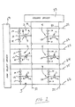
- FIG. 1 is a schematic circuit diagram of an active matrix liquid crystal display (AMLCD) including a MIM diode drive scheme according to an embodiment of this invention.
- AMLCD active matrix liquid crystal display
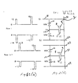
- Figure 2(a) is a circuit diagram of two different pixels of Figure 1, on different rows, according to a first embodiment of this invention.
- Figure 2(b) illustrates four separate voltage v. time graphs which correspond to the four select lines illustrated in Figure 2(a) [i.e. how these pixels are driven in operation].
- Figure 3(a) is a circuit diagram of two different pixels of Figure 1, on different rows, according to a second embodiment of this invention.
- Figure 3(b) illustrates four separate voltage v. time graphs which correspond to the four select lines in Figure 3(a), according to the second embodiment of this invention.
- Figure 4(a) is a circuit diagram of two pixels of Figure 1, according to a third embodiment of this invention.
- Figure 4(b) illustrates four separate voltage v. time graphs which correspond to the select or row lines illustrated in Figure 4(a), according to the third embodiment of this invention.
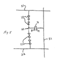
- Figure 5 is a circuit diagram of a pixel of Figure 1, according to a fourth embodiment of this invention, wherein a pair of MIM diodes are provided on each branch (i.e. four MIMs per pixel).
- Figure 6 is a top view of a matrix array of pixels, and corresponding MIM diodes, according to the Figure 5 embodiment of this invention (showing the row lines and four MIMs per pixel), wherein the column of data lines on the opposite substrate are not shown.
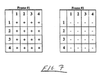
- Figure 7 are a pair of graphs illustrating row inversion as discussed herein.
- the "+” and “-” signs in the Fig. 7 graphs represent, with the display operating in AC, the polarity of the voltage at the pixel node V with respect to the voltage on the opposite electrode (made up of patterned columns of ITO to which the data is applied) across the LC layer.
- the voltage at pixel node V is +5 volts and the voltage on the opposite pixel electrode across the LC layer is 0 volts, then a "+” sign would be used in Figure 7 (although the V does not remain constant during each frame as it floats, except during select periods).
- Figure 8 are a pair of graphs illustrating row inversion useful with embodiments of this invention, wherein each row of pixels in the display has a given polarity in each frame, with the next row having the opposite polarity, and wherein polarity for each row of pixels changes for the next frame.
- Figure 9 are a pair of graphs illustrating column inversion, where column inversion is the same as row inversion, except that each column of pixels has its own polarity in a given frame and then changes polarity for the next frame.
- Figure 10 are a pair of graphs illustrating dot(pixel) inversion from one display frame to the next.
- Figure 11 is a schematic Pspice simulation circuit for one row in a 28 in. SVGA single MIM LCD configuration for comparison with dual MIM designs of this invention.
- "Pspice” is simulation software, available from MicroSim, of California, for simulating circuits.
- Figure 12 is a schematic Pspice simulation circuit for one row in 28 in. SVGA dual MIM LCD in accordance with certain embodiments of this invention.
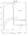
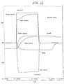
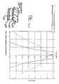
- Figure 17 is a three dimensional graph, illustrating pixel voltage variation (mV) [vertical axis] as a function of both row resistance (kohm) and column resistance (kohm), for the single MIM display of Figures 11, 13, and 14. This graph is used for purposes of comparison with the dual MIM graph of Fig. 18.
- Figure 18 is a three dimensional graph of the dual MIM circuit of Figs. 12, 15, and 16, illustrating pixel voltage variation (mV) [vertical axis] as a function of both row resistance (kohm) and column resistance (kohm).
- Figure 19(a) is a voltage (volts) versus current (amps) graph, with characteristics normalized to 30 um x 30 um, of a 30 x 30 MIM diode using amorphous silicon nitride (dotted line) as the insulator and of a similar diamond line carbon insulated MIM device (solid line).
- Figure 19(b) is a side cross sectional view of a MIM diode or a TFD diode in accordance with certain embodiments of this invention.
- Figure 20(a) is a graph illustrating center return video driving.
- Figure 20(b) is a graph illustrating bipolar video driving.
- FIG. 1 is a schematic circuit diagram of an AMLCD according to an embodiment of this invention.
- the AMLCD includes a plurality of pixels 1-6 arranged in a matrix array on the active substrate of the display.
- Pixel 1 includes liquid crystal layer 7 sandwiched between individual pixel electrode 8 and common electrode 9, as well as MIM diodes 10 and 11 which are coupled to one another and to pixel electrode 8 via common node 12.
- Common node 12 is in communication with each of MIM diodes 10, 11, via branches extending therefrom, as well as with pixel electrode 8.
- Each of the other pixels 2-6 also includes a pair of MIM diodes 10, 11 coupled at a common node 12, as well as LC material 7 sandwiched between pixel electrodes 8 and 9.
- the common electrode 9 in each pixel is in electrical communication with a column or data line 31, 32.
- the Figure 1 display further includes row or select lines 21-26 that are driven and selected by row select driver 27, and column or data lines 31 and 32 which are selected and driven by column driver 33.
- Select lines 21-26 are all substantially parallel to one another and are oriented in a first direction, while data lines 31-32 are also substantially parallel to one another, but are oriented in a second direction that is substantially orthogonal to the first direction.
- select lines 21-26 are substantial orthogonal to data lines 31-32 across the active matrix array.
- a pair of row or select lines is provided for each pixel, while only a single column or data line is utilized for each pixel.
- the AMLCD includes additional pixels as well as additional select and data address lines sufficient in number so as to form a usable image for displaying to a viewer (e.g. see Figure 6).
- Each of the pixels 1-6 herein is substantially identical.
- the insulator in MIM diodes 10-11 is conventionally either anodized Ta 2 O 5 (tantalum oxide) or Si-rich SiN x (silicon nitride) grown by plasma enhanced chemical vapor deposition (CVD).
- SiN x diodes have steeper current voltage characteristics than Ta 2 O 5 diodes and a lower diode capacitance. Thus, SiN x diodes are more attractive for higher resolution displays.
- SiN x diodes suffer from device degradation and spacial non-uniformity.
- the pixel circuits described herein thus are designed so as to have greatly increased tolerance for spacial and temporal variations of MIM diode current-voltage characteristics, as SiN x MIM diodes are preferred in certain embodiments.
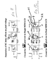
- a row of pixels (e.g. pixels 1 and 4) is selected by applying simultaneously opposite polarity pulses to select lines 21 and 22 while at the same time applying data voltage to the column lines in that particular row as desired.
- the polarity of the voltage pulses on any given select line remain constant for that line.
- select line 21 for example, the polarity of pulses thereon will always be positive while the polarity of the pulses on the corresponding select line 22 will always be negative. This allows for less complex circuitry to be utilized. This is the case with all pixels disclosed herein.
- SiN x MIM diodes are utilized in this third embodiment.
- Two MIM diodes are connected to each LC pixel, and two separate select lines (21 and 22 for pixel 1).
- a row of pixels is selected by applying simultaneously opposite polarity pulses 41 and 42 of substantially equal magnitude, to the pixel, while applying data voltage to the corresponding column line 31.
- SiN x MIM diodes 10-11 any variation in the current-voltage characteristic of the MIM device over time, with temperature, or across the display area will result in a variation of the LC voltage.
- the thickness and composition (i.e. Si/N ratio) of the SiN x layer determines in part the diode's current-voltage curve. Because it is difficult to control thickness and composition accurately over large area, the current voltage curve of such SiN x MIM diodes 10-11 will vary significantly across large area displays.
- the SiN x diode current decreases, when pulsed in the on-state for an extended period of time, leading to image retention in conventional circuits.
- MIM current also depends on temperature, a non-uniform heating of the display will result from pixel voltage variation across the display area. Circuits herein overcome these problems.
- a select voltage 41 of about 15 volts is applied to select line 21, while simultaneously a select voltage 42 of -15 volts is , applied to select line 22, while a data voltage of 5 volts is applied to column or data line 31.
- These voltages may range from 10-30 volts for line 21, and from -10 to -30 for line 22.
- the 4(a) circuit of pixel 1, when these signals are applied, the pixel charging saturates rapidly at the data voltage and is virtually independent of MIM current variations up to 10X.
- the pixel charging saturates quickly, because the voltage across each MIM device 10, 11 is still 15 volts when the pixel voltage approaches the data voltage, so that a significant on-current keeps flowing until the select pulses are switched off.
- the pixel voltage shift at termination of the select pulses 41 and 42 is substantially eliminated in the illustrated circuit, because the capacitive feed through voltage of diodes loll substantially cancels out.
- the illustrated Figure 4(a) circuit can still charge the pixel almost completely.
- Figures 1 and 2(a)-2(b) While the third embodiment shown in Figures 4(a)-4(b), when operated in a simultaneous scan mode, has numerous advantages over prior art MIM LCD technology including much improved spacial and temporal gray shade control and uniformity, faster response time, reduced image retention and cross-talk, and increased tolerance for RC delays on the row and column lines, the drawback of the Figure 4(a)-4(b) embodiment is that it needs to have at least a ten volt swing on the data line in order to obtain sufficient voltage across LC 7 and the relatively high voltage that can occur across MIM diodes in the off-state (during the non-select period).
- V D varies between -2.5 and +2.5 volts in this example
- V s may range from about 10-30 volts
- V offset may range from about 2-4 volts.
- the maximum voltage across each MIM diode 10, 11 in the off-state is about 7 to 8 volts, resulting in improved charge retention in the LC 7 capacitance in each pixel.
- the cancellation of the pixel voltage shift from the two diodes is not complete in this drive scheme, because the opposite polarity pulses on lines 21 and 22, for example, are not of equal magnitude.
- the data voltage is applied in row inversion mode [i.e. the data signal voltage polarity is charged for each row].
- pixel 1 is driven as follows.
- a pulse of V s - V offset (e.g. 15 volts - 3 volts equals 12 volts) is applied to select line 21, while a pulse of -V s - V offset (e.g. -15 volts - 3 volts equals -18 volts) is simultaneously applied to select line 22, while at the same time a data voltage of 2.5 volts is applied to column line 31.
- This charges the LC capacitance of each pixel.
- a 30 volt differential is applied between select lines 21 and 22, after each select pulsing, each node branch has a drop of 15 volts.
- node 12 When MIM diodes 10-11 are switched off, node 12 floats and follows the column line voltage so that, for example, if -2.5 volts are applied to column line 31, the voltage at node 12 goes to -8 volts, while select line 21 and 22 are at 0 volts.
- the circuit enables the system to use less voltage on the column lines (this saves cost and circuit complexity), and allows less voltage variation at both node 12 and on the column lines so that there is less leakage through MIM diodes 10 and 11. Minimizing leakage through diodes 10-11 in the MIM off-state is desirable as will be appreciated by those of skill in the art.
- a voltage of V s + V offset (e.g. 15 volts + 3 volts equals 18 volts) is applied to select line 21, while a voltage of -V s + V offset (-15 volts + 3 volts equals -12 volts) is applied to select line 22, while a data voltage is applied to column line 31.
- the signal on line 21 goes back to V s - V offset and the signal on line 22 goes back to -V s - V offset for the next pulsing.
- the pulsing on each of lines 21 and 22 alternate between these two values for subsequent frames when the AMLCD is on.
- Each pixel in the active matrix array is driven in a similar manner.
- the Figure 2(a)-2(b) embodiment of this invention allows the circuit to have a smaller voltage swing on the data line (i.e. column line 31), while still obtaining sufficient voltage across liquid crystal material 7 in each pixel and limiting leakage through the MIM diodes 10-11.
- the voltage swing on line 31 is reduced to 5 volts (from 2.5 volts to -2.5 volts) which is an improvement over the 10 volt swing shown in Figure 4(a).
- the Figure 2(a)-2(b) embodiment has a reduced number of voltage levels applied to the select lines, than does the prior art discussed in the Background Section of this application.
- the voltage drop on the column or data lines is no greater than about 6 volts, preferably less than or equal to about 5 volts, while the voltage swing between corresponding select lines is no greater than about 32 volts, and is preferably less than or equal to about 30 volts.
- FIGS 5-6 illustrate a fourth embodiment of this invention, where, in contrast to the first three embodiments discussed above, a pair of separate MIM diodes are provided in each node branch. Therefore, we have four MIM diodes per pixel.
- This design improves the symmetrical nature of the circuit, and results in improved driving characteristics when, as discussed above, the pulse signals on each select line always have the same polarity.
- twin MIM diodes 10, 11, connected back-to-back in each branch the pixel voltage on pixel electrode 8, and at common node 12, goes exactly to: (V 1 + V 2 ) ⁇ 2, at the end of the select time, wherein V 1 is the voltage pulse on line 21 and V 2 is the voltage pulse on line 22. This is perfectly symmetrical.
- Figure 6 is a top view illustrating a matrix array of pixel electrodes 8, select lines 21, 22, and MIM diodes 10, 11, according to the Figure 5 embodiment of this invention.
- This Figure 5-6 embodiment may use the drive schemes in any of the other embodiments of this invention (e.g. see Figures 2(b)-4(b)).
- FIG. 8 Each of the above discussed and/or illustrated embodiments of this invention is compatible with row inversion (e.g. Fig. 8) and frame inversion (e.g. Fig. 7) types driving schemes for LCD applications. This is in contrast to the Maeda '728 patent which, unfortunately, is limited to frame inversion applications. Additionally, the Figure 4(a) and 4(b) embodiment of this invention discussed above is compatible with both column inversion driving and pixel inversion driving. Center return video (e.g. 10 to 14 volt data driver) is typically used with the Fig. 4(a)-4(b) embodiment of this invention, while bipolar video (e.g. 5 volt data driver) is typically used with the other embodiments of this invention.
- Center return video e.g. 10 to 14 volt data driver
- bipolar video e.g. 5 volt data driver
- Figure 7 shows frame inversion, as all of the pixels in the display have the same polarity (+ or -) during a given frame, and the polarity of each pixel is changed for subsequent frames. Two frames, one after the other, are shown in Figure 7.
- Frame inversion is undesirable in that it leads to top-to-bottom shading, cross talk, and flicker in LCD applications and is therefore almost never used.
- Flicker is typically defined by variation in luminance of more than a certain percentage (e.g. 5-10%) at frequency less than about 40 Hz. Because flicker can be reduced by spatial averaging, the solution to the flicker problems associated with frame inversion are row inversion, column inversion, and/or pixel inversion described below.
- Figure 8 shows an embodiment of row inversion, where one row of pixels in the display has a "+" polarity for an entire frame and another adjacent row of pixels has an opposite "-" polarity during that frame.
- each row of pixels alternates polarity in each frame, and the polarity in each pixel changes for each frame so that if a pixel is "+" in one frame, it will be "-" in the next frame (this is the case for the illustrated embodiments of Figs. 7-10 herein).
- Two frames, one after the other, are shown in Fig. 8.
- every other row is of the same polarity so that adjacent rows in a given frame are of opposite polarity.
- adjacent rows may be of the same polarity (e.g. where the first and second rows are "+”, the third and fourth rows “-”, the fifth and sixth rows “+”, etc.
- row inversion reduces flicker due to spatial averaging, and reduces vertical cross talk. All MIM embodiments of this invention may be driven using these row inversion techniques, as they are preferable.
- Figure 9 illustrates column inversion, which reduces flicker and horizontal cross talk.
- the Figure 4(a)-4(b) embodiment of this invention may utilize column inversion driving techniques.
- each column of pixels in the LCD has the same polarity in a given frame, and then switches polarity for the next frame.
- adjacent columns of pixels in a given frame have opposite polarities "+" and "-".
- Figure 10 illustrates pixel or dot inversion, which results in high image quality due to reduction in vertical and horizontal cross talk.
- Pixel or dot inversion is impossible with a pixel having only one MIM in it (i.e. a single MIM circuit).
- Pixel inversion can only be done in a pixel having at least two MIMs, such as in the instant dual MIM circuit having two select lines per pixel. Flicker is also reduced with pixel inversion.
- the Fig. 4(a)-4(b) embodiment of this invention may utilized pixel or dot inversion. Again, the polarity of each pixel changes from frame to subsequent frame, and all pixels of the display in a given frame are not of the same polarity (this is also the case with row and column inversion).
- polarity is defined as the polarity of the voltage at the pixel node V p (or 12) with respect to the voltage on the opposite electrode 9 across the LC layer 7.
- the opposite electrodes 9 across the display are made up of patterned columns of ITO or the like to which data signals are applied.
- bipolar video ( Figure 20(b))
- ON and OFF state of the pixel are respectively, e.g. +2.5 volts and -2.5 volts during the first frame, and -2.5 volts and +2.5 volts during the second frame, etc.
- the additional voltage needed to fully turn on the LC comes from biasing the node 12 between the two MIM diodes to e.g. -3 V and +3 V respectively during first and second select times.
- the polarity of data for ON and OFF state and polarity for bias at the node 12 are simply reversed to obtain row inversion.
- the OFF state is 0 V and the ON state is +5 V and -5 V during first and second frames, respectively, and the voltage applied to the node 12 between the MIM diodes during the select time can stay at zero at all times.
- SSDM LCDs of this invention are substantially insensitive to variations in MIM characteristics as to RC delays on rows as well as column as will be further discussed below.
- circuit simulations shown in Figs. 11 and 12 of 28 inch diagonal SVGA displays were performed.
- Figure 11 is a circuit simulation of one row of a conventional single MIM LCD
- Figure 12 is a circuit simulation of one row of pixels of a SSDM LCD according to an embodiment of this invention.
- the Figure 12 SSDM device is superior relative to the single MIM Figure 11 device. Certain simulation parameters used in both the Fig. 11 and Fig.
- FIG. 11 shows the Pspice simulation circuit for the single and dual MIM displays, respectively.
- An exponential model is a fairly good representation of the actual measured curves and is easy to implement in Pspice.
- a more accurate physics/based model for the conduction mechanism is Frenkel-Poole conduction.
- Figures 13-18 were obtained from the Figure 11-12 simulations.
- Figures 15 and 16 show the same curves for the SSDM circuit of Figure 12 according to embodiments of this invention. Note the differences between the single MIM graphs of Figs. 13-14 and the dual MIM graphs of Figs. 15-16. Meanwhile, Fig. 17 shows a three dimensional plot of the pixel voltage variation of the Fig. 11 circuit, and Fig. 18 shows a three dimensional plot of the pixel voltage variation of the Fig. 12 circuit, with each of Figs.
- V pix V pix, - + Ts ⁇ 0 I mim [V mim (t)]dt/C 1c , where V pix, - is the pixel voltage immediately before the select pulse, Ts is the select time, I mim is the MIM current which depends on the MIM voltage V mim , and C 1c is the capacitance of the LC or liquid crystal material in the pixel.
- V mim (t) V select (t) -V data (t) -V 1c (t).
- V mim (t) V select (t) -V data (t) -V 1c (t).
- the above two equations show that the pixel voltage V pix depends on the initial pixel voltage V pix, - , on the MIM current-voltage characteristics, on Clc (which in turn depends on voltage, time and cell gap of the lc), and also on the detailed shapes of the select pulse and data pulse. In other words, select and data pulse distortion along the buslines or address lines will have a substantial effect on the pixel voltage. This is clear from the charging plots for the single MIM circuit in Figs. 13 and 14.
- the pixel voltage V pix is independent of the detailed MIM IV curves (i.e. current/voltage curves) and independent of the detailed shape of the select and data pulse, as long as pixel charging saturates.
- the IV curves of the two branches in the SSDM circuit e.g. see Figs. 1-5 which illustrate the two MIM branches in each pixel
- the dual MIM switch functions as an analog switch, when operated in a simultaneous select mode as illustrated herein, and transfers the data voltage exactly to the pixel, much like a TFT.
- Pixel charging saturates better in the dual MIM switch than in a TFT, because the switch current in the dual MIM circuit herein remains relatively high when the pixel voltage approaches the data voltage, whereas in a TFT the current goes to zero when the pixel voltage approaches the data voltage (i.e. when the source/drain voltage goes to zero).
- the pixel voltage shift, proportional to C mim /C 1c in the single MIM circuit is absent in the dual MIM circuit due to cancellation of the capacitive feedthrough in the two branches.
- V pix V data
- Condition (a) is met because of the proximity of the MIM diodes in the two branches of one pixel.
- a SiN x diode IV curves can vary across the display area as a result of temperature variations, SiN x thickness and composition (e.g. Si/N ratio) variations or dimensional variations in the MIM area, they can be normally assumed not to vary over a few hundred microns within a pixel.
- Condition (b) may require the two select voltages to have equal magnitudes across the entire display.
- the load on the rows in the SSDM circuit has both a capacitive and a resistive component (as compared to TFT arrays, where the load is purely capacitive as long as the gate nitride is not leaky).
- a row resistance of e.g. 2 kohm gives good uniformity in the 28 in.
- Dual MIM SVGA display and corresponds to an Al (aluminum) row busline with a width of 30 ⁇ m and a thickness of 0.3 ⁇ m.
- the row line metal is the last metal deposited and functions also as the top electrode for the MIM diode in the current process in certain embodiments.
- a thicker Al layer of e.g. 1 ⁇ m makes even larger displays feasible.
- amorphous C:N (carbon nitride) alloy film is used as the insulator or semi-insulator of each MIM diode 10, 11.
- This insulator (or semi-insulator) 104 is typically located between two opposing electrodes of the TFD or MIM diode, as shown in Fig. 19(b).
- a MIM or TFD diode, invented herein, including a-C:N as the semi insulator, has current voltage characteristics which are desirable for a switch in a metal-insulator-metal (MIM) LCD display or x-ray imaging device.
- MIM metal-insulator-metal
- This a-C:N alloy is a material that emulates its crystalline component beta-CN. The latter has a hardness value greater than that of diamond and is very stable to heat, light, and electrical stress.
- the high field electrical conduction of a-C:N has been studied over a temperature range of 300-500K, and current is found to increase exponentially with the electric field.
- the exponential factor is found to increase linearly with the inverse of temperature in this range.
- the activation energy of the conductivity is also found to be strongly field dependent and to increase linearly with electric field.
- a-C:N thin films show I-V characteristics with higher gradient than Si-rich Si x N y of comparable thickness.
- a-C:N does not show any substantial photoconductivity even at light photons with energies larger than its bandgap of about 2.4 eV.
- the electrical relative permittivity is about 3-4. This means that MIM devices 10, 11 with larger area can be fabricated hence the use of a scanning projector for large 2D array fabrication, instead of more expensive aligners.
- the allow may include or consist essentially of on carbon (C), nitrogen (N), and hydrogen (H).
- C carbon
- N nitrogen
- H hydrogen
- in the alloy from about 20-60% of the atoms in the alloy are nitrogen atoms (more preferably from about 40-60%)
- from about 40-80% of the atoms in the alloy are carbon atoms (more preferably from about 40-60%)
- hydrogen, which is optional is provided in the alloy from about 0-25% of the atoms in the alloy are hydrogen atoms (more preferably from about 0-15%, and most preferably from about 1-5%).
- a-C:N films with the above characteristics can be synthesized at low substrate temperatures ( ⁇ 100 degrees C) by two techniques: (i) growth from solid carbon, and (ii) growth from gas phase. Growth from solid carbon - sputtering of graphite targets by Ar+ ions with simultaneous low energy (e.g. from about 100-500 eV) N+ peening or assisted bombardment at ion beam densities of approximately 0.5 mA/cm 2 . These conditions are favorable for the growth of a-C:N films with relatively high N/C atomic ratios from about 0.4 to 0.6.
- the use of electron energy loss spectroscopy initially shows that while the carbon was hybriseed tetrahedrally the nitrogen was sp2 hybridised giving unpolarized covalent C-N bonds. Further electron diffraction studies show that the films have a nano crystals of beta-C-N embedded in an essentially amorphous matrix.
- the films show hardness of about 60 Gpa and electrical resistivity of above 7 x 10 12 ohm-cm.
- the alloy has an electrical resistivity of from about 5 x 10 7 to 7 x 10 12 .
- the optical bandgap was above 3 eV, and in certain embodiments the alloy's Tauc bandgap is at least about 3.0.
- the alloy has a hardness of at least about 50 Gpa, and more preferably of at least about 70 Gpa.
- the films can be deposited using a plasma enhanced CVD (chemical vapor deposition) method in which acetelyne and NF 3 /NH 3 gas mixtures are introduced into a chamber via separate gas lines.
- the power density ⁇ 500 W/m 2 and substrate temperature ⁇ 350K.
- nitrogen incorporation into the carbon matrix causes a reduction in the bandgap of the carbon network.
- CF 4 /O 2 as an etchant gas may be used.
- FIG 19(b) shows a TFD (e.g. MIM diode 10, 11) on substantially transparent glass substrate 101 according to an embodiment of this invention.
- this TFD may be a MIM diode 10, 11 wherein bottom electrode 102 and top electrode 103 are both of metals (e.g. Mo) while insulator or semi-insulator layer 104 disposed therebetween is of a material such as a-C:N as discussed above.
- a non-metal such as indium-tin-oxide (ITO) may be used as one or both of the electrode(s) 102/103 in the diode of Fig. 19(b).
- ITO indium-tin-oxide
- the TFD includes ITO as bottom electrode 102 and Mo as top electrode 103, with either diamond-like carbon, a-C:N, or silicon rich liquid nitride as semi-insulator 104.
- MIM diodes are nonlinear resistance elements.
- the liquid crsytal is sealed between two opposing substrates on which column and row lines are formed, respectively, and the nonlinear resistance elements (e.g. MIMs) and one set of pixel electrodes are formed on the inner surface of one of the substrates 101.
- the other pixel electrode, opposite the pixel electrode formed on substrate 101, is formed on an opposing substrate on the other side of the LC layer as shown in U.S. Pat.
- the non linear resistance diodes 10, 11 are electrically connected between one of the pixel electrodes and the select lines on substrate 101. It is noted that in nonlinear resistance elements, a very small current flows even during the retention period, so that stored data is affected gradually by data signals.
- layer 104 of TFD (e.g. MIM diode) 10, 11 of Fig. 19(b) may be of nanocrystalline carbon, or of polycrystalline carbon.
- Semi-insulators of MIM or TFD diodes have typically been of Ta 2 O 5 or PECVD grown Si-rich SiN x :H.
- a drawback of these two materials is their relatively high dielectric constant values: about 23 and 8.5 respectively for Ta 2 O 5 and SiN x :H, respectively.
- these electronic materials being binary and ternary alloys, are prone to issues such as spatial homogeneity and temporal degradation when used within an active device such as a diode in this case.
- the simultaneous scan dual TFD or MIM [SSDM] approach shown and discussed above in Figs. 1-10, 12, 15, 16, 18, 19(b), and 20 is/are provided in order to overcome the effects of spatial, temporal, and temperature dependent variations in TFD and MIM device characteristics.
- I-V symmetry or symmetricity of the TFD or MIM devices 10, 11 should be good. Symmetry can be achieved by using two diodes in series per branch as shown in Fig. 5 for example. This approach however implies that the switching voltage needed per pixel is doubled and consequently is at the fringe of operability of presently available drivers.
- the present embodiment uses semi-insulators in the form of poly-crystalline diamond and nanocrystalline carbon thin films optionally containing small amounts of N and F dopant atoms for TFD or MIM semi-insulator layer 104 [see Fig. 19(b)]. Additional desirable features of these two films include (i) low dielectric constant of less than about 4.0, preferably between about 3.0 and 4.0, which implies a lower capacitive coupling and kickback voltage; (ii) wide bandgap E diamond of approximately 5.3-5.7 eV, preferably aboaut 5.5 eV, and E d1c >3eV, which results in high transparency and virtually no photoconductivity because the density of states (DOS) is above 10 18 cm -3 eV -1 pinning the Fermi-Level in the gap; (iii) high dielectric breakdown strength E > 5 x 10 6 V cm -1 ; (iv) highly symmetric I-V (current-voltage) characteristics requiring half of the switching voltage needed for Si-rich SiN x
- a MIM or TFD can be made by providing a substrate 101 such as glass, depositing and patterning a first electrode 102 array (e.g.
- MIM or TFD devices 10, 11 can be made in accordance with this invention.
- MIM and TFD diodes 10, 11 herein are non-linear resistance elements, and are also bi-directional threshold devices.
- Figure 19(a) is a voltage versus current (amps) graph illustrating I-V characteristics of a carbon MIM (solid line) versus a a-Si:N MIM (dotted line). Note the low variation of voltage as a function of current for the carbon MIM diode of Fig. 19(a).
Landscapes
- Engineering & Computer Science (AREA)
- Chemical & Material Sciences (AREA)
- Crystallography & Structural Chemistry (AREA)
- Physics & Mathematics (AREA)
- Computer Hardware Design (AREA)
- General Physics & Mathematics (AREA)
- Theoretical Computer Science (AREA)
- Liquid Crystal (AREA)
- Control Of Indicators Other Than Cathode Ray Tubes (AREA)
- Liquid Crystal Display Device Control (AREA)
Applications Claiming Priority (4)
| Application Number | Priority Date | Filing Date | Title |
|---|---|---|---|
| US08/935,678 US6225968B1 (en) | 1997-09-23 | 1997-09-23 | Method and system for addressing LCD including diodes |
| US935678 | 1997-09-23 | ||
| US09/035,819 US6243062B1 (en) | 1997-09-23 | 1998-03-06 | Method and system for addressing LCD including thin film diodes |
| US35819 | 1998-03-06 |
Publications (3)
| Publication Number | Publication Date |
|---|---|
| EP0910062A2 true EP0910062A2 (fr) | 1999-04-21 |
| EP0910062A3 EP0910062A3 (fr) | 1999-10-06 |
| EP0910062B1 EP0910062B1 (fr) | 2009-08-26 |
Family
ID=26712526
Family Applications (1)
| Application Number | Title | Priority Date | Filing Date |
|---|---|---|---|
| EP98117949A Expired - Lifetime EP0910062B1 (fr) | 1997-09-23 | 1998-09-22 | Méthode et dispositif d'adressage de panneaux d'affichage à cristaux liquides à diodes à couche mince |
Country Status (3)
| Country | Link |
|---|---|
| US (1) | US6243062B1 (fr) |
| EP (1) | EP0910062B1 (fr) |
| CA (1) | CA2246837C (fr) |
Cited By (6)
| Publication number | Priority date | Publication date | Assignee | Title |
|---|---|---|---|---|
| EP0951008A3 (fr) * | 1998-03-06 | 2000-01-05 | OIS Optical Imaging Systems, Inc. | Méthode et dispositif d'adressage de panneaux d'affichage à cristaux liquides à diodes à couche mince |
| US6243062B1 (en) | 1997-09-23 | 2001-06-05 | Ois Optical Imaging Systems, Inc. | Method and system for addressing LCD including thin film diodes |
| JP2005148756A (ja) * | 2003-11-18 | 2005-06-09 | Samsung Electronics Co Ltd | 薄膜ダイオード表示板及びこれを含む液晶表示装置 |
| EP1536408A3 (fr) * | 2003-11-25 | 2006-09-06 | Sanyo Electric Co., Ltd. | Affichage à cristal liquide |
| EP1579266A4 (fr) * | 2001-06-20 | 2007-10-03 | Citala Ltd | Commutateurs plans de faible epaisseur et leur applications |
| CN103236496A (zh) * | 2013-04-18 | 2013-08-07 | 福州大学 | 一种叠层结构的三端有源器件 |
Families Citing this family (33)
| Publication number | Priority date | Publication date | Assignee | Title |
|---|---|---|---|---|
| JPH1130975A (ja) * | 1997-05-13 | 1999-02-02 | Oki Electric Ind Co Ltd | 液晶表示装置の駆動回路及びその駆動方法 |
| US7304632B2 (en) * | 1997-05-13 | 2007-12-04 | Oki Electric Industry Co., Ltd. | Liquid-crystal display driving circuit and method |
| KR100338007B1 (ko) * | 1997-09-30 | 2002-10-11 | 삼성전자 주식회사 | 액정 표시 장치 및 그의 구동 방법 |
| TW521241B (en) * | 1999-03-16 | 2003-02-21 | Sony Corp | Liquid crystal display apparatus, its driving method, and liquid crystal display system |
| US6563482B1 (en) * | 1999-07-21 | 2003-05-13 | Semiconductor Energy Laboratory Co., Ltd. | Display device |
| US6469684B1 (en) * | 1999-09-13 | 2002-10-22 | Hewlett-Packard Company | Cole sequence inversion circuitry for active matrix device |
| KR100917324B1 (ko) * | 2002-11-16 | 2009-09-11 | 엘지디스플레이 주식회사 | 모바일 폰용 액정표시장치 |
| KR100920355B1 (ko) * | 2003-03-28 | 2009-10-07 | 삼성전자주식회사 | 액정 표시 장치용 박막 다이오드 표시판 및 이를 포함하는액정 표시 장치 |
| US20050083321A1 (en) * | 2003-10-17 | 2005-04-21 | Scanvue Technologies Llc | Shared select line display |
| KR100925471B1 (ko) * | 2003-10-29 | 2009-11-06 | 삼성전자주식회사 | 반투과형 액정 표시 장치용 박막 다이오드 표시판 |
| KR100951359B1 (ko) * | 2003-10-29 | 2010-04-09 | 삼성전자주식회사 | 박막 다이오드 표시판 및 그 제조 방법 |
| KR101026802B1 (ko) * | 2003-11-18 | 2011-04-04 | 삼성전자주식회사 | 액정 표시 장치 및 그 구동 방법 |
| US6967118B2 (en) * | 2004-03-09 | 2005-11-22 | Hewlett-Packard Development Company, L.P. | Process for creating Metal-Insulator-Metal devices |
| US20050225543A1 (en) * | 2004-04-07 | 2005-10-13 | Scanvue Technologies Llc | Display circuit having asymmetrical nonlinear resistive elements |
| TWI282876B (en) * | 2004-10-07 | 2007-06-21 | Au Optronics Corp | TFD LED device with high aperture ratio |
| US7160745B2 (en) * | 2004-10-28 | 2007-01-09 | Hewlett-Packard Development Company, L.P. | Metal-insulator-metal device |
| US20060091496A1 (en) * | 2004-10-28 | 2006-05-04 | Hewlett-Packard Development Company, Lp | Metal-insulator-metal device |
| US8013826B1 (en) | 2005-06-25 | 2011-09-06 | Nongqiang Fan | Method of driving active matrix displays having nonlinear elements in pixel elements |
| KR101244656B1 (ko) * | 2006-06-19 | 2013-03-18 | 엘지디스플레이 주식회사 | 액정표시장치 |
| US7969276B2 (en) * | 2007-04-25 | 2011-06-28 | Scanvue Technologies, Llc | Thin film varistor array |
| US8358258B1 (en) * | 2008-03-16 | 2013-01-22 | Nongqiang Fan | Active matrix display having pixel element with light-emitting element |
| US20120081347A1 (en) * | 2010-09-30 | 2012-04-05 | Apple Inc. | Low power inversion scheme with minimized number of output transitions |
| US8674918B1 (en) * | 2011-09-05 | 2014-03-18 | Nongqiang Fan | Method of driving active matrix displays |
| US8698723B1 (en) * | 2011-09-05 | 2014-04-15 | Nongqiang Fan | Method of driving active matrix displays |
| US8941640B2 (en) | 2012-06-08 | 2015-01-27 | Apple Inc. | Differential VCOM resistance or capacitance tuning for improved image quality |
| JP2018524642A (ja) * | 2015-07-24 | 2018-08-30 | オレゴン ステイト ユニバーシティ | アクティブなサブピクセル装置としてアモルファス金属非線形抵抗を使用した面内スイッチング液晶ディスプレイ・バックプレーン |
| CN111919302B (zh) | 2018-03-30 | 2025-01-14 | 非结晶公司 | 非晶金属薄膜晶体管 |
| US10634949B1 (en) * | 2018-10-17 | 2020-04-28 | a.u. Vista Inc. | Display systems and methods involving MIM diodes |
| US11138944B2 (en) * | 2018-12-06 | 2021-10-05 | Xianyang Caihong Optoelectronics Technology Co., Ltd | Pixel matrix driving device and display device |
| TWI850295B (zh) * | 2018-12-07 | 2024-08-01 | 美商非結晶公司 | 用於基於二極體之顯示器背板之方法及電路及電子顯示器 |
| TWI912327B (zh) | 2020-06-12 | 2026-01-21 | 美商非結晶公司 | 用於電子裝置之包括非線性組件的電路 |
| CN117116224B (zh) * | 2023-08-31 | 2026-01-09 | 长沙惠科光电有限公司 | 显示面板和显示装置 |
| CN121260121A (zh) * | 2025-12-03 | 2026-01-02 | 青岛信芯微电子科技股份有限公司 | 显示设备及设备控制方法 |
Family Cites Families (11)
| Publication number | Priority date | Publication date | Assignee | Title |
|---|---|---|---|---|
| NL8502663A (nl) | 1985-09-30 | 1987-04-16 | Philips Nv | Weergeefinrichting met verbeterde aansturing. |
| US4731610A (en) | 1986-01-21 | 1988-03-15 | Ovonic Imaging Systems, Inc. | Balanced drive electronic matrix system and method of operating the same |
| FR2605778B1 (fr) | 1986-10-24 | 1990-11-16 | Thomson Csf | Panneau de visualisation a cristaux liquides et procede d'inscription des donnees sur ce panneau |
| GB2217891A (en) | 1988-04-29 | 1989-11-01 | Philips Electronic Associated | Matrix display device |
| US5142390A (en) | 1989-02-23 | 1992-08-25 | Ricoh Company, Ltd. | MIM element with a doped hard carbon film |
| EP0434627A3 (en) | 1989-12-18 | 1991-10-23 | Ois Optical Imaging Systems, Inc. | Balanced drive symmetric mim diode configuration for liquid crystal displays and method of operating same |
| JP2630663B2 (ja) | 1990-03-09 | 1997-07-16 | セイコー電子工業株式会社 | 電気光学装置 |
| JPH04122982A (ja) | 1990-09-13 | 1992-04-23 | Seiko Instr Inc | 電気光学装置の駆動方法 |
| WO1996021881A1 (fr) * | 1995-01-13 | 1996-07-18 | Flat Panel Display Co. (Fpd) B.V. | Dispositif d'affichage a cristaux liquides |
| JP3110980B2 (ja) * | 1995-07-18 | 2000-11-20 | インターナショナル・ビジネス・マシーンズ・コーポレ−ション | 液晶表示装置の駆動装置及び方法 |
| US6243062B1 (en) | 1997-09-23 | 2001-06-05 | Ois Optical Imaging Systems, Inc. | Method and system for addressing LCD including thin film diodes |
-
1998
- 1998-03-06 US US09/035,819 patent/US6243062B1/en not_active Expired - Lifetime
- 1998-09-08 CA CA002246837A patent/CA2246837C/fr not_active Expired - Fee Related
- 1998-09-22 EP EP98117949A patent/EP0910062B1/fr not_active Expired - Lifetime
Cited By (10)
| Publication number | Priority date | Publication date | Assignee | Title |
|---|---|---|---|---|
| US6243062B1 (en) | 1997-09-23 | 2001-06-05 | Ois Optical Imaging Systems, Inc. | Method and system for addressing LCD including thin film diodes |
| EP0951008A3 (fr) * | 1998-03-06 | 2000-01-05 | OIS Optical Imaging Systems, Inc. | Méthode et dispositif d'adressage de panneaux d'affichage à cristaux liquides à diodes à couche mince |
| US6222596B1 (en) | 1998-03-06 | 2001-04-24 | Ois Optical Imaging Systems, Inc. | Thin film diode including carbon nitride alloy semi-insulator and method of making same |
| EP1579266A4 (fr) * | 2001-06-20 | 2007-10-03 | Citala Ltd | Commutateurs plans de faible epaisseur et leur applications |
| JP2005148756A (ja) * | 2003-11-18 | 2005-06-09 | Samsung Electronics Co Ltd | 薄膜ダイオード表示板及びこれを含む液晶表示装置 |
| EP1536408A3 (fr) * | 2003-11-25 | 2006-09-06 | Sanyo Electric Co., Ltd. | Affichage à cristal liquide |
| CN100371963C (zh) * | 2003-11-25 | 2008-02-27 | 三洋电机株式会社 | 显示装置 |
| US7532189B2 (en) | 2003-11-25 | 2009-05-12 | Sanyo Electric Co., Ltd. | Liquid crystal display capable of making flicker difficult to be observed and reducing power consumption |
| CN103236496A (zh) * | 2013-04-18 | 2013-08-07 | 福州大学 | 一种叠层结构的三端有源器件 |
| CN103236496B (zh) * | 2013-04-18 | 2015-08-12 | 福州大学 | 一种叠层结构的三端有源器件 |
Also Published As
| Publication number | Publication date |
|---|---|
| CA2246837C (fr) | 2007-01-16 |
| EP0910062A3 (fr) | 1999-10-06 |
| CA2246837A1 (fr) | 1999-03-23 |
| EP0910062B1 (fr) | 2009-08-26 |
| US6243062B1 (en) | 2001-06-05 |
Similar Documents
| Publication | Publication Date | Title |
|---|---|---|
| EP0910062B1 (fr) | Méthode et dispositif d'adressage de panneaux d'affichage à cristaux liquides à diodes à couche mince | |
| US6222596B1 (en) | Thin film diode including carbon nitride alloy semi-insulator and method of making same | |
| US5227900A (en) | Method of driving ferroelectric liquid crystal element | |
| US4747671A (en) | Ferroelectric optical modulation device and driving method therefor wherein electrode has delaying function | |
| US5117298A (en) | Active matrix liquid crystal display with reduced flickers | |
| US5337171A (en) | Electro-optical device | |
| US5608420A (en) | Liquid crystal display apparatus | |
| US6225968B1 (en) | Method and system for addressing LCD including diodes | |
| US5541747A (en) | Electro-optical device utilizing a liquid crystal having a spontaneous polarization | |
| EP0479291B1 (fr) | Méthode et dispositif de commande d'un appareil d'affichage à cristaux liquides | |
| JP2816549B2 (ja) | 電気光学装置 | |
| EP0526076B1 (fr) | Dispositif d'affichage à matrice active à cristaux liquides | |
| JPH06230746A (ja) | 能動マトリックス液晶表示システム及び該システムの動作方法 | |
| DE69120564T2 (de) | Verfahren zur Ansteuerung eines ferroelektrischen Flüssigkristallelementes und ferroelektrische Flüssigkristallanzeige | |
| US20030006954A1 (en) | Driving method for liquid crystal device | |
| JP2990232B2 (ja) | 液晶電気光学装置 | |
| US20050083283A1 (en) | Differentiating circuit display | |
| EP0461648B1 (fr) | Afficheur à cristal liquide à matrice du type métal-isolant-métal sans image rémanente | |
| JP3161707B2 (ja) | 電気光学装置 | |
| JPWO1994018600A1 (ja) | 非線形抵抗素子およびその製造方法ならびに液晶表示装置 | |
| den Boer et al. | Dual Branch MIM Array Technology for Low‐Cost AMLCDs | |
| JPH05110100A (ja) | アクテイブマトリクス型液晶表示装置 | |
| JP2578941B2 (ja) | アクティブマトリクス液晶表示装置の駆動方法 | |
| den Boer | 6.2: A Select Line Driver for the Offset‐Scan‐and‐Hold Dual Select Diode AMLCDs | |
| JP3431874B2 (ja) | 投射型ディスプレイおよび反射型ディスプレイ |
Legal Events
| Date | Code | Title | Description |
|---|---|---|---|
| PUAI | Public reference made under article 153(3) epc to a published international application that has entered the european phase |
Free format text: ORIGINAL CODE: 0009012 |
|
| AK | Designated contracting states |
Kind code of ref document: A2 Designated state(s): DE FR GB NL |
|
| AX | Request for extension of the european patent |
Free format text: AL;LT;LV;MK;RO;SI |
|
| PUAL | Search report despatched |
Free format text: ORIGINAL CODE: 0009013 |
|
| AK | Designated contracting states |
Kind code of ref document: A3 Designated state(s): AT BE CH CY DE DK ES FI FR GB GR IE IT LI LU MC NL PT SE |
|
| AX | Request for extension of the european patent |
Free format text: AL;LT;LV;MK;RO;SI |
|
| 17P | Request for examination filed |
Effective date: 20000405 |
|
| AKX | Designation fees paid |
Free format text: DE FR GB NL |
|
| RAP1 | Party data changed (applicant data changed or rights of an application transferred) |
Owner name: GUARDIAN INDUSTRIES CORP. |
|
| 17Q | First examination report despatched |
Effective date: 20060421 |
|
| GRAP | Despatch of communication of intention to grant a patent |
Free format text: ORIGINAL CODE: EPIDOSNIGR1 |
|
| GRAS | Grant fee paid |
Free format text: ORIGINAL CODE: EPIDOSNIGR3 |
|
| GRAA | (expected) grant |
Free format text: ORIGINAL CODE: 0009210 |
|
| AK | Designated contracting states |
Kind code of ref document: B1 Designated state(s): DE FR GB NL |
|
| REG | Reference to a national code |
Ref country code: GB Ref legal event code: FG4D |
|
| REF | Corresponds to: |
Ref document number: 69841088 Country of ref document: DE Date of ref document: 20091008 Kind code of ref document: P |
|
| PLBE | No opposition filed within time limit |
Free format text: ORIGINAL CODE: 0009261 |
|
| STAA | Information on the status of an ep patent application or granted ep patent |
Free format text: STATUS: NO OPPOSITION FILED WITHIN TIME LIMIT |
|
| 26N | No opposition filed |
Effective date: 20100527 |
|
| REG | Reference to a national code |
Ref country code: NL Ref legal event code: SD Effective date: 20110608 Ref country code: GB Ref legal event code: 732E Free format text: REGISTERED BETWEEN 20110602 AND 20110608 |
|
| REG | Reference to a national code |
Ref country code: FR Ref legal event code: TP |
|
| REG | Reference to a national code |
Ref country code: DE Ref legal event code: R082 Ref document number: 69841088 Country of ref document: DE Representative=s name: 2K PATENTANWAELTE BLASBERG KEWITZ & REICHEL, P, DE |
|
| REG | Reference to a national code |
Ref country code: DE Ref legal event code: R082 Ref document number: 69841088 Country of ref document: DE Representative=s name: 2K PATENTANWAELTE BLASBERG KEWITZ & REICHEL PA, DE Effective date: 20110930 Ref country code: DE Ref legal event code: R082 Ref document number: 69841088 Country of ref document: DE Representative=s name: 2K PATENTANWAELTE BLASBERG KEWITZ & REICHEL, P, DE Effective date: 20110930 Ref country code: DE Ref legal event code: R081 Ref document number: 69841088 Country of ref document: DE Owner name: CHIMEI INNOLUX CORP., TW Free format text: FORMER OWNER: GUARDIAN INDUSTRIES CORP., AUBURN HILLS, MICH., US Effective date: 20110930 |
|
| REG | Reference to a national code |
Ref country code: FR Ref legal event code: PLFP Year of fee payment: 19 |
|
| PGFP | Annual fee paid to national office [announced via postgrant information from national office to epo] |
Ref country code: NL Payment date: 20160926 Year of fee payment: 19 Ref country code: GB Payment date: 20160927 Year of fee payment: 19 |
|
| PGFP | Annual fee paid to national office [announced via postgrant information from national office to epo] |
Ref country code: FR Payment date: 20160926 Year of fee payment: 19 |
|
| PGFP | Annual fee paid to national office [announced via postgrant information from national office to epo] |
Ref country code: DE Payment date: 20160928 Year of fee payment: 19 |
|
| REG | Reference to a national code |
Ref country code: DE Ref legal event code: R119 Ref document number: 69841088 Country of ref document: DE |
|
| REG | Reference to a national code |
Ref country code: NL Ref legal event code: MM Effective date: 20171001 |
|
| GBPC | Gb: european patent ceased through non-payment of renewal fee |
Effective date: 20170922 |
|
| PG25 | Lapsed in a contracting state [announced via postgrant information from national office to epo] |
Ref country code: NL Free format text: LAPSE BECAUSE OF NON-PAYMENT OF DUE FEES Effective date: 20171001 |
|
| REG | Reference to a national code |
Ref country code: FR Ref legal event code: ST Effective date: 20180531 |
|
| PG25 | Lapsed in a contracting state [announced via postgrant information from national office to epo] |
Ref country code: DE Free format text: LAPSE BECAUSE OF NON-PAYMENT OF DUE FEES Effective date: 20180404 Ref country code: GB Free format text: LAPSE BECAUSE OF NON-PAYMENT OF DUE FEES Effective date: 20170922 |
|
| PG25 | Lapsed in a contracting state [announced via postgrant information from national office to epo] |
Ref country code: FR Free format text: LAPSE BECAUSE OF NON-PAYMENT OF DUE FEES Effective date: 20171002 |