EP0910236A2 - Elektronisches Gerät - Google Patents
Elektronisches Gerät Download PDFInfo
- Publication number
- EP0910236A2 EP0910236A2 EP98307896A EP98307896A EP0910236A2 EP 0910236 A2 EP0910236 A2 EP 0910236A2 EP 98307896 A EP98307896 A EP 98307896A EP 98307896 A EP98307896 A EP 98307896A EP 0910236 A2 EP0910236 A2 EP 0910236A2
- Authority
- EP
- European Patent Office
- Prior art keywords
- electronic apparatus
- circuit board
- printed circuit
- side plate
- frame member
- Prior art date
- Legal status (The legal status is an assumption and is not a legal conclusion. Google has not performed a legal analysis and makes no representation as to the accuracy of the status listed.)
- Granted
Links
Images




Classifications
-
- H—ELECTRICITY
- H05—ELECTRIC TECHNIQUES NOT OTHERWISE PROVIDED FOR
- H05K—PRINTED CIRCUITS; CASINGS OR CONSTRUCTIONAL DETAILS OF ELECTRIC APPARATUS; MANUFACTURE OF ASSEMBLAGES OF ELECTRICAL COMPONENTS
- H05K3/00—Apparatus or processes for manufacturing printed circuits
- H05K3/30—Assembling printed circuits with electric components, e.g. with resistors
- H05K3/32—Assembling printed circuits with electric components, e.g. with resistors electrically connecting electric components or wires to printed circuits
- H05K3/34—Assembling printed circuits with electric components, e.g. with resistors electrically connecting electric components or wires to printed circuits by soldering
- H05K3/3405—Edge mounted components, e.g. terminals
-
- H—ELECTRICITY
- H05—ELECTRIC TECHNIQUES NOT OTHERWISE PROVIDED FOR
- H05K—PRINTED CIRCUITS; CASINGS OR CONSTRUCTIONAL DETAILS OF ELECTRIC APPARATUS; MANUFACTURE OF ASSEMBLAGES OF ELECTRICAL COMPONENTS
- H05K7/00—Constructional details common to different types of electric apparatus
- H05K7/14—Mounting supporting structure in casing or on frame or rack
-
- H—ELECTRICITY
- H05—ELECTRIC TECHNIQUES NOT OTHERWISE PROVIDED FOR
- H05K—PRINTED CIRCUITS; CASINGS OR CONSTRUCTIONAL DETAILS OF ELECTRIC APPARATUS; MANUFACTURE OF ASSEMBLAGES OF ELECTRICAL COMPONENTS
- H05K9/00—Screening of apparatus or components against electric or magnetic fields
- H05K9/0007—Casings
- H05K9/002—Casings with localised screening
- H05K9/0039—Galvanic coupling of ground layer on printed circuit board [PCB] to conductive casing
-
- H—ELECTRICITY
- H05—ELECTRIC TECHNIQUES NOT OTHERWISE PROVIDED FOR
- H05K—PRINTED CIRCUITS; CASINGS OR CONSTRUCTIONAL DETAILS OF ELECTRIC APPARATUS; MANUFACTURE OF ASSEMBLAGES OF ELECTRICAL COMPONENTS
- H05K2201/00—Indexing scheme relating to printed circuits covered by H05K1/00
- H05K2201/09—Shape and layout
- H05K2201/09145—Edge details
-
- H—ELECTRICITY
- H05—ELECTRIC TECHNIQUES NOT OTHERWISE PROVIDED FOR
- H05K—PRINTED CIRCUITS; CASINGS OR CONSTRUCTIONAL DETAILS OF ELECTRIC APPARATUS; MANUFACTURE OF ASSEMBLAGES OF ELECTRICAL COMPONENTS
- H05K2201/00—Indexing scheme relating to printed circuits covered by H05K1/00
- H05K2201/20—Details of printed circuits not provided for in H05K2201/01 - H05K2201/10
- H05K2201/2018—Presence of a frame in a printed circuit or printed circuit assembly
-
- H—ELECTRICITY
- H05—ELECTRIC TECHNIQUES NOT OTHERWISE PROVIDED FOR
- H05K—PRINTED CIRCUITS; CASINGS OR CONSTRUCTIONAL DETAILS OF ELECTRIC APPARATUS; MANUFACTURE OF ASSEMBLAGES OF ELECTRICAL COMPONENTS
- H05K3/00—Apparatus or processes for manufacturing printed circuits
- H05K3/30—Assembling printed circuits with electric components, e.g. with resistors
- H05K3/32—Assembling printed circuits with electric components, e.g. with resistors electrically connecting electric components or wires to printed circuits
- H05K3/34—Assembling printed circuits with electric components, e.g. with resistors electrically connecting electric components or wires to printed circuits by soldering
- H05K3/3447—Lead-in-hole components
Definitions
- the present invention relates to an electronic apparatus such as a television tuner.
- Figs. 8 through 10 show a conventional electronic apparatus.
- a frame 21 is formed of metal and open on the upper and lower sides. It is equipped with a side plate 21a, engagement members 21b formed by denting part of the side plate 21a, and support members 21d formed by providing U-shaped holes 21c in the side plate 21a.
- a rectangular printed circuit board 22 is equipped with a conductive pattern 23 including a wiring pattern 23a and a grounding pattern 23b.
- the grounding pattern 23b is provided in the vicinity of the periphery of the printed circuit board 22 and close to the frame 21, connecting to the frame 21 at a nearer position.
- This printed circuit board 22 is inserted into the frame 21, and its lower portion is engaged with the engagement members 21b. It is pressed by support members 21d bent at the upper portions thereof, the support members 21d and the grounding patterns 23b being soldered to each other with solder 24, whereby it is mounted to the frame 21.
- the printed circuit board 22 when mounting the printed circuit board 22 to the frame 21, the printed circuit board 22 is first inserted into the frame 21, and the printed circuit board 22 is engaged with the engagement members 21b.
- the support members 21d are bent by a jig (not shown) from the direction P, and, as shown in Fig. 10(B), the support members 21 protrude into the frame 21 so that the printed circuit board 22 is supported by the support members 21d.
- the support members 21d and the grounding patterns 23b are manually soldered to each other as indicated at 24 by using a soldering iron 25 and a wire solder 26, thereby connecting the grounding patterns 23b to the frame 21.
- the grounding patterns 23b must be formed so as to be positioned inside the frame 21.
- a width H for soldering 24 is required, with the result that the size of the frame 21 and that of the printed circuit board 22 are rather large.
- an electronic apparatus comprising a frame member and a printed circuit board portion, the frame member having a metal side plate, the side plate including a notched portion at the upper end thereof and a support member erect in the notched portion, the printed circuit board having a conductive pattern on the surface thereof and a protrusion in its outer periphery, a through-hole being provided at the base of the protrusion, a conductive pattern being provided on the surface around the through-hole, the protrusion of the printed circuit board protruding to the exterior of the frame member from the notched portion of the side plate with the support member of the side plate being inserted into the through-hole of the printed circuit board, the support member being soldered to the conductive pattern and connected thereto.
- a swelled portion is provided on the support member of the side plate, the support member of the side plate being inserted into the through-hole of the printed circuit board in a forced-fit state due to the swelled portion.
- the height of the support member of the side plate is such that it does not protrude from the upper end of the side plate.
- Fig. 1 is a perspective view of an electronic apparatus according to the present invention
- Fig. 2 is an essential-part sectional view of the electronic apparatus of the present invention
- Figs. 3(A) and 3(B) are diagrams illustrating a method of manufacturing the electronic apparatus of the present invention
- Fig. 4 is an essential-part perspective view showing an electronic apparatus according to a second embodiment of the present invention
- Fig. 5 is an essential-part sectional view of Fig. 4
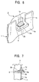
- Fig. 6 is an essential-part perspective view showing an electronic apparatus according to a third embodiment of the present invention
- Fig. 7 is an essential-part sectional view of Fig. 6.
- the electronic apparatus of the present invention includes a rectangular metal frame member 1, which is equipped with a side plate 1a that is open on the upper and lower sides and protruding support portions 1c formed by forming notched portions 1b from the upper end of the side plate 1a.
- the open portion of the frame member 1 is covered so as to electrically shield the interior of the frame member 1.
- the rectangular printed circuit board 2 includes rectangular protrusions 2a protruding from the outer periphery, holes 2b provided in the protrusions 2a, and conducting patterns 3 consisting of a wiring pattern 2a formed on the printed circuit board 2 and grounding patterns 3b.
- the grounding patterns 3b are formed in the periphery of the printed circuit board 2 and around the holes 2b.
- the protrusions 2a are positioned in the notched portions 1b, and the support portions 1c are passed through the holes 2b, the lower portions of the protrusions 2a being engaged with the bottom surfaces of the notched portions 1b.
- the support portions 1c and the grounding patterns 3b are soldered to each other as indicated at 4, whereby the printed circuit board 2 is mounted to the frame member 1.
- the protrusions 2a of the printed circuit board 2 are first positioned in the notched portions 1b of the frame member 1, and the support portions 1c are passed through the holes 2, the lower portions of the protrusions 2a being temporarily engaged with the bottom surfaces of the notched portions 1b.
- this frame member 1 is conveyed to a solder paste applying machine by a belt, and a nozzle 5 of the solder paste applying machine is positioned above the support portion 1c, causing solder paste 6 to drop from the nozzle 5.
- solder paste 6 flows down to the grounding pattern 3b, so that the solder paste 6 exists between the support member 1c and the grounding pattern 3b.
- Figs. 4 and 5 show the second embodiment of the electronic apparatus of the present invention.
- the support portion 1c is provided with a protrusion 1d, and this protrusion 1d is forced into the hole 2b of the printed circuit board 2 to temporarily engage the printed circuit board 2 with the frame member 1.
- this embodiment is the same as that of the above-described embodiment.
- the components which are the same as those of the above embodiment are indicated by the same reference numerals, and a description thereof will be omitted.
- Figs. 6 and 7 show the third embodiment of the electronic apparatus of the present invention.
- the position of the upper end of the support portion 2c is lower than the upper end of the side plate 1a, so that, when the cover 7, indicated by a two-dot chain line in Fig. 7, is placed in position, the upper end of the support portion 1c does not abut the cover 7.
- this embodiment is the same as that of the first embodiment, so the components which are the same as those of the first embodiment are indicated by the same reference numerals, and a description of such components will be omitted.
- the notched portion 1b extending from the upper end of the side plate 1a is provided to form the protruding support portion 1c, whereby it is possible to provide an electronic apparatus which is simpler in construction, improved in productivity and less expensive as compared with the conventional electronic apparatus.
- the support portion 1c is passed through the hole 2b of the printed circuit board 2, and the support portion 1c and the grounding pattern 3b is soldered to each other as indicated at 4, the width h for soldering 4 in the frame member 1 can be reduced, whereby the frame 1 and the printed circuit board 2 can be reduced in size, thereby making it possible to provide a small-sized electronic apparatus.
- the printed circuit board 2 is temporarily engaged by providing the support portion 1c with the protrusion 1d and forcing the protrusion 1d into the hole 2b of the printed circuit board 2, the position of the printed circuit board 2 with respect to the frame member 1 is stabilized, whereby it is possible to provide an electronic apparatus in which the support portion 1c and the grounding pattern 3b are reliably soldered to each other.
- the support portion 1c separated from the side plate 1a at the upper end does not come into contact with or move away from the cover 7 when rattling is generated due to vibrations, etc. of the electronic apparatus, whereby it is possible to provide a high performance electronic apparatus.
- solder paste 6 is dropped from above the support portion 1c formed by forming the notched portion 1b from the upper end of the side plate 1a to thereby cause the solder paste 6 to exist between the support portion 1c and the grounding pattern 3b, so that manufacturing by an automatic machine is possible, whereby it is possible to provide an inexpensive electronic apparatus having satisfactory productivity.
Landscapes
- Engineering & Computer Science (AREA)
- Microelectronics & Electronic Packaging (AREA)
- Manufacturing & Machinery (AREA)
- Shielding Devices Or Components To Electric Or Magnetic Fields (AREA)
- Mounting Of Printed Circuit Boards And The Like (AREA)
- Casings For Electric Apparatus (AREA)
- Accessory Devices And Overall Control Thereof (AREA)
Applications Claiming Priority (3)
| Application Number | Priority Date | Filing Date | Title |
|---|---|---|---|
| JP28327097 | 1997-10-16 | ||
| JP283270/97 | 1997-10-16 | ||
| JP9283270A JPH11121946A (ja) | 1997-10-16 | 1997-10-16 | 電子機器、並びに電子機器の製造方法 |
Publications (3)
| Publication Number | Publication Date |
|---|---|
| EP0910236A2 true EP0910236A2 (de) | 1999-04-21 |
| EP0910236A3 EP0910236A3 (de) | 2000-01-05 |
| EP0910236B1 EP0910236B1 (de) | 2003-12-10 |
Family
ID=17663290
Family Applications (1)
| Application Number | Title | Priority Date | Filing Date |
|---|---|---|---|
| EP98307896A Expired - Lifetime EP0910236B1 (de) | 1997-10-16 | 1998-09-29 | Elektronisches Gerät |
Country Status (7)
| Country | Link |
|---|---|
| EP (1) | EP0910236B1 (de) |
| JP (1) | JPH11121946A (de) |
| KR (1) | KR100272805B1 (de) |
| CN (1) | CN1175567C (de) |
| DE (1) | DE69820384T2 (de) |
| MY (1) | MY120238A (de) |
| TW (1) | TW438212U (de) |
Cited By (1)
| Publication number | Priority date | Publication date | Assignee | Title |
|---|---|---|---|---|
| EP1257160A1 (de) * | 2001-05-12 | 2002-11-13 | Siemens Aktiengesellschaft | Verfahren zum Herstellen eines aus einem Abschirmgehäuse und einer Leiterplatte bestehenden elektronischen Geräts |
Families Citing this family (3)
| Publication number | Priority date | Publication date | Assignee | Title |
|---|---|---|---|---|
| JP4626457B2 (ja) * | 2005-09-14 | 2011-02-09 | パナソニック株式会社 | ケースとこれを用いた電子機器 |
| JP5257786B2 (ja) * | 2009-09-11 | 2013-08-07 | 株式会社Jvcケンウッド | 基板支持装置 |
| JP7463252B2 (ja) * | 2020-10-29 | 2024-04-08 | ホシデン株式会社 | 電子機器用充電器 |
Family Cites Families (4)
| Publication number | Priority date | Publication date | Assignee | Title |
|---|---|---|---|---|
| DE8120399U1 (de) * | 1981-07-11 | 1981-11-19 | Rohde & Schwarz GmbH & Co KG, 8000 München | Hochfrequenzdichte Baugruppe für Geräte der elektrischen Nachrichtentechnik |
| JPS60106379U (ja) * | 1983-12-26 | 1985-07-19 | アルプス電気株式会社 | 電子機器用ケ−ス |
| JPH0642398Y2 (ja) * | 1989-03-03 | 1994-11-02 | 株式会社村田製作所 | 貫通コンデンサの取付け構造 |
| JP2830702B2 (ja) * | 1993-07-16 | 1998-12-02 | 関西日本電気株式会社 | ケースの基板への取り付け構造 |
-
1997
- 1997-10-16 JP JP9283270A patent/JPH11121946A/ja active Pending
-
1998
- 1998-09-22 TW TW089202426U patent/TW438212U/zh not_active IP Right Cessation
- 1998-09-25 MY MYPI98004412A patent/MY120238A/en unknown
- 1998-09-29 EP EP98307896A patent/EP0910236B1/de not_active Expired - Lifetime
- 1998-09-29 DE DE69820384T patent/DE69820384T2/de not_active Expired - Lifetime
- 1998-10-15 KR KR1019980043107A patent/KR100272805B1/ko not_active Expired - Fee Related
- 1998-10-16 CN CNB981204368A patent/CN1175567C/zh not_active Expired - Fee Related
Cited By (2)
| Publication number | Priority date | Publication date | Assignee | Title |
|---|---|---|---|---|
| EP1257160A1 (de) * | 2001-05-12 | 2002-11-13 | Siemens Aktiengesellschaft | Verfahren zum Herstellen eines aus einem Abschirmgehäuse und einer Leiterplatte bestehenden elektronischen Geräts |
| US6712639B2 (en) | 2001-05-12 | 2004-03-30 | Siemens Aktiengesellschaft | Method for manufacturing an electronic apparatus having a shielding assembly and a printed wire board |
Also Published As
| Publication number | Publication date |
|---|---|
| KR19990037107A (ko) | 1999-05-25 |
| EP0910236A3 (de) | 2000-01-05 |
| MY120238A (en) | 2005-09-30 |
| EP0910236B1 (de) | 2003-12-10 |
| CN1215254A (zh) | 1999-04-28 |
| TW438212U (en) | 2001-05-28 |
| CN1175567C (zh) | 2004-11-10 |
| DE69820384T2 (de) | 2004-05-27 |
| KR100272805B1 (ko) | 2000-11-15 |
| DE69820384D1 (de) | 2004-01-22 |
| JPH11121946A (ja) | 1999-04-30 |
Similar Documents
| Publication | Publication Date | Title |
|---|---|---|
| US6572412B2 (en) | Control device and soldering method | |
| US4747019A (en) | Feedthrough capacitor arrangement | |
| US5792994A (en) | Device for mounting a component | |
| EP1122825B1 (de) | Auf einem Substrat montierter Kontaktstift | |
| EP0910236B1 (de) | Elektronisches Gerät | |
| JP2639280B2 (ja) | 高密度回路モジュールの製造方法 | |
| JPH0745346A (ja) | チップ部品用ソケット | |
| EP0957665B1 (de) | Elektronische Einrichtung | |
| KR0166431B1 (ko) | 회로 모듈 제조방법 | |
| JP2863981B2 (ja) | ラグ端子およびその取り付け方法 | |
| US5097389A (en) | Structure for fixing feedthrough capacitor in high-frequency device and manufacturing method of high-frequency device | |
| JP3333811B2 (ja) | 高周波機器の製造方法 | |
| JP3924122B2 (ja) | 電子機器 | |
| JPH08293687A (ja) | 外部接続用コネクタを備えたシールド電気製品の製造方法及びシールド電気製品 | |
| KR19990003854U (ko) | 프레임체와 프린트기판의 접속구조 | |
| JPH10233592A (ja) | シールド板の取付け方法及び取付け構造 | |
| JPH05290908A (ja) | プリント基板に対する端子板の接続構造 | |
| KR890008391Y1 (ko) | 프린트 기판상의 안테나선 연결장치 | |
| JP3623637B2 (ja) | 電子機器 | |
| JPH071741Y2 (ja) | F型コネクタ取付構体 | |
| JPH10214645A (ja) | コネクタ | |
| JPH0317484Y2 (de) | ||
| KR200226389Y1 (ko) | 기판의아일릿설치구조 | |
| JPH07122875A (ja) | シールドケース | |
| JPH05226013A (ja) | プリント配線板用導電部品 |
Legal Events
| Date | Code | Title | Description |
|---|---|---|---|
| PUAI | Public reference made under article 153(3) epc to a published international application that has entered the european phase |
Free format text: ORIGINAL CODE: 0009012 |
|
| AK | Designated contracting states |
Kind code of ref document: A2 Designated state(s): DE GB |
|
| AX | Request for extension of the european patent |
Free format text: AL;LT;LV;MK;RO;SI |
|
| PUAL | Search report despatched |
Free format text: ORIGINAL CODE: 0009013 |
|
| AK | Designated contracting states |
Kind code of ref document: A3 Designated state(s): AT BE CH CY DE DK ES FI FR GB GR IE IT LI LU MC NL PT SE |
|
| AX | Request for extension of the european patent |
Free format text: AL;LT;LV;MK;RO;SI |
|
| 17P | Request for examination filed |
Effective date: 20000210 |
|
| AKX | Designation fees paid |
Free format text: DE GB |
|
| GRAH | Despatch of communication of intention to grant a patent |
Free format text: ORIGINAL CODE: EPIDOS IGRA |
|
| GRAS | Grant fee paid |
Free format text: ORIGINAL CODE: EPIDOSNIGR3 |
|
| GRAA | (expected) grant |
Free format text: ORIGINAL CODE: 0009210 |
|
| AK | Designated contracting states |
Kind code of ref document: B1 Designated state(s): DE GB |
|
| REG | Reference to a national code |
Ref country code: GB Ref legal event code: FG4D |
|
| REF | Corresponds to: |
Ref document number: 69820384 Country of ref document: DE Date of ref document: 20040122 Kind code of ref document: P |
|
| PLBE | No opposition filed within time limit |
Free format text: ORIGINAL CODE: 0009261 |
|
| STAA | Information on the status of an ep patent application or granted ep patent |
Free format text: STATUS: NO OPPOSITION FILED WITHIN TIME LIMIT |
|
| 26N | No opposition filed |
Effective date: 20040913 |
|
| PGFP | Annual fee paid to national office [announced via postgrant information from national office to epo] |
Ref country code: DE Payment date: 20100930 Year of fee payment: 13 |
|
| PGFP | Annual fee paid to national office [announced via postgrant information from national office to epo] |
Ref country code: GB Payment date: 20110826 Year of fee payment: 14 |
|
| GBPC | Gb: european patent ceased through non-payment of renewal fee |
Effective date: 20120929 |
|
| REG | Reference to a national code |
Ref country code: DE Ref legal event code: R119 Ref document number: 69820384 Country of ref document: DE Effective date: 20130403 |
|
| PG25 | Lapsed in a contracting state [announced via postgrant information from national office to epo] |
Ref country code: GB Free format text: LAPSE BECAUSE OF NON-PAYMENT OF DUE FEES Effective date: 20120929 Ref country code: DE Free format text: LAPSE BECAUSE OF NON-PAYMENT OF DUE FEES Effective date: 20130403 |