EP0913954A2 - Circuit et méthode pour le transfert de signaux entre des dispositifs semiconducteurs - Google Patents
Circuit et méthode pour le transfert de signaux entre des dispositifs semiconducteurs Download PDFInfo
- Publication number
- EP0913954A2 EP0913954A2 EP98304051A EP98304051A EP0913954A2 EP 0913954 A2 EP0913954 A2 EP 0913954A2 EP 98304051 A EP98304051 A EP 98304051A EP 98304051 A EP98304051 A EP 98304051A EP 0913954 A2 EP0913954 A2 EP 0913954A2
- Authority
- EP
- European Patent Office
- Prior art keywords
- power supply
- circuit
- bits
- data stream
- serial data
- Prior art date
- Legal status (The legal status is an assumption and is not a legal conclusion. Google has not performed a legal analysis and makes no representation as to the accuracy of the status listed.)
- Withdrawn
Links
Images

Classifications
-
- H—ELECTRICITY
- H04—ELECTRIC COMMUNICATION TECHNIQUE
- H04B—TRANSMISSION
- H04B3/00—Line transmission systems
- H04B3/54—Systems for transmission via power distribution lines
- H04B3/548—Systems for transmission via power distribution lines the power on the line being DC
-
- H—ELECTRICITY
- H04—ELECTRIC COMMUNICATION TECHNIQUE
- H04B—TRANSMISSION
- H04B2203/00—Indexing scheme relating to line transmission systems
- H04B2203/54—Aspects of powerline communications not already covered by H04B3/54 and its subgroups
- H04B2203/5462—Systems for power line communications
- H04B2203/547—Systems for power line communications via DC power distribution
-
- H—ELECTRICITY
- H04—ELECTRIC COMMUNICATION TECHNIQUE
- H04B—TRANSMISSION
- H04B2203/00—Indexing scheme relating to line transmission systems
- H04B2203/54—Aspects of powerline communications not already covered by H04B3/54 and its subgroups
- H04B2203/5462—Systems for power line communications
- H04B2203/5483—Systems for power line communications using coupling circuits
-
- H—ELECTRICITY
- H04—ELECTRIC COMMUNICATION TECHNIQUE
- H04B—TRANSMISSION
- H04B2203/00—Indexing scheme relating to line transmission systems
- H04B2203/54—Aspects of powerline communications not already covered by H04B3/54 and its subgroups
- H04B2203/5462—Systems for power line communications
- H04B2203/5491—Systems for power line communications using filtering and bypassing
Definitions
- the invention relates generally to semiconductor devices and, more particularly, to inter-device signal transfer circuitry and methodology.
- pins are used to supply power and ground reference potentials to the chip.
- CMOS or TTL semiconductor device receives a supply potential of 5 V through one pin, and a ground potential of 0 V through another pin.
- Integrated circuits implemented in other forms of logic, such as ECL, receive other reference potential levels as supply and ground and may even receive a plurality of supply potentials.
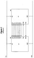
- Pins are also used to carry electrical signals between chips. Specifically, pins provide electrical connections for transferring bit data from one chip to another. Conventional chips use multiple pins to input and output multiple bit data. For example, in Figure 1, conventional IC 100 transmits 8-bit parallel data (a "byte") to IC 110 using transmit data pins D0 to D7 and transmit data strobe pin TDS. Transmit data strobe pin TDS is used for signalling that the multiple-bit data on pins D0 to D7 are valid. IC 110 receives the byte at pins D0 to D7, when signaled by received data strobe RDS. Pins D0 to D7 in Figure 1 are bidirectional, allowing for data to be both transmitted and received through the same pins.
- IC 100 further comprises receive data strobe pin RDS for receiving a signal indicating that data on pins D0 to D7 are ready to be read.
- receive data strobe pin RDS for receiving a signal indicating that data on pins D0 to D7 are ready to be read.
- the number of pins required for signalling is ten and the number of pins required for receiving reference potentials is two, for a total of twelve pins for each chip.
- Pins although necessary, consume space on the chip and often require expensive packaging. Therefore, a need exists to greatly reduce the number of pins required by semiconductor devices.
- a circuit for transferring signals between chips comprises a power supply pin.
- the power supply pin couples the chip to a power supply line.
- a first filter is coupled to the power supply pin and functional elements of the chip for supplying a low-frequency signal from the power supply line to the chip functional elements.
- a second filter is coupled between the power supply pin and a transceiver for supplying the transceiver with high-frequency signal components of the power supply line.
- the transceiver coupled to the second filter and chip functional elements, is configured for serializing and deserializing multiple bit data received from and supplied to the power supply line for signal transfer between chips.
- a network of semiconductor devices comprises a common power supply line, with each semiconductor device having a power supply pin coupled to the power supply line.
- a first filter is coupled to the power supply pin and functional elements of the chip for supplying a low-frequency signal from the power supply line to the chip functional elements.
- a second filter is coupled between the power supply pin and a transceiver for supplying the transceiver with high-frequency signal components from the power supply line.
- the transceiver coupled to the second filter and chip functional elements, is configured for serializing and deserializing multiple bit data for the chip functional elements as high-frequency components from and to the power supply line.
- a method for communicating between a source semiconductor device and a destination semiconductor device comprises the step of serializing bits into a serial data stream and outputting the serial data stream to a power supply line.
- the method includes filtering out the serial data stream as high frequency components from the power supply and deserializing the serial data stream.
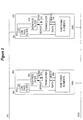
- a serial link connection is implemented over the power supply line V cc between IC 200 and IC 210.
- the serial link connection allows parallel data, conventionally signalled by multiple pins, to be transmitted and received serially through the power supply pin.
- the multiple, parallel pin configuration is eliminated in favor of a single power supply pin.
- IC 200 comprises low pass filter 202 and high pass filter 204, each coupled to power supply line V cc .
- Low pass filter 202 is coupled to functional elements 208, which implements the functionality of the semiconductor device.
- the chip functional elements may comprise computational or signal processing circuitry.
- Transceiver 206 is coupled to high pass filter 204 and chip functional elements 208.
- IC 210 comprises low pass filter 212, high pass filter 214, transceiver 216, and chip functional elements 218, all of which are coupled and operate in a manner similar to the respective components of IC 200.
- IC 200 transmits multiple bit data to IC 210 through power supply line V cc as follows.
- Chip functional elements 208 sends parallel bit data to transceiver 206, which serializes the multiple bit data into a serial data stream.
- Transceiver 206 outputs the serial data stream at a very fast rate, e.g., 7 GHz.
- the serial data stream is sent through high pass filter 204 as high frequency components to power supply line V cc .
- IC 210 receives the serial data stream as a high frequency component of power supply line V cc .
- High pass filter 214 extracts high frequency components of power supply line V cc and transmits the high frequency components as the serial data stream to transceiver 216.
- Transceiver 216 receives the serial data stream and deserializes the serial data stream back into the transmitted parallel bit data. In this manner, a multiple bit signal is transmitted through power supply line V cc .
- the power supply reference potential is a low frequency component of power supply line V cc . Accordingly, low pass filter 202 and low pass filter 212 extract the low frequency component to provide a steady power supply voltage to the components of IC 200 and IC 210, respectively.
- high pass filter 214 and low pass filter 202 are implemented as standard, analog, first-order RC filters.
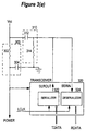
- low pass filter 300 comprises resistor 302 and capacitor 304 coupled in series in that order from power line V cc to ground.
- the output of low pass filter 300 is tapped from the node coupling resistor 302 and capacitor 304.
- High pass filter 310 comprises capacitor 312 and resistor 314 coupled in series in that order from power supply line V cc to ground.
- the output of high pass filter 310 is tapped from the node coupling capacitor 312 and resistor 314.
- low pass filter 300 and high pass filter 310 are implemented by well known techniques in the art of metal-oxide-semiconductor technology. Since the power supply line signal comprises only a DC steady state component and a very high frequency component, up to 7 GHz, the bandwidths of low pass filter 300 and high pass filter 310 can be very large without adversely affecting their performance. Consequently, there is much flexibility in choosing resistive and capacitive values for the filters depending on manufacturing constraints.
- transceiver 300 comprises serializer 302 and deserializer 304, both of which receive local clock signal LCLK.
- Serializer 302 further receives parallel transmit data TDATA and outputs serial data output SEROUT.
- Deserializer 304 further receives serial data input SERIN and outputs parallel receive data RDATA.
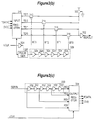
- the serialization function of transceiver 300 comprises input register 310 which is configured to latch parallel data bits TDATA(3:0) on receipt of local clock signal LCLK.
- Input register 310 provides a plurality of outputs, each of which is coupled to an input terminal of a respective switch 312-318 in a gating network comprising a plurality of MOS switches.
- the output terminals of the plurality of switches 312-318 are connected to a common node. Also coupled to the common node is pull-up load device 320 and output inverter 322.
- the serialization function further comprises pulse generator 326 which receives local clock signal LCLK and the output of adjustable delay element 324 , which also receives local clock signal LCLK.
- the output of pulse generator 326 is coupled to delay line 328, which comprises a plurality of adjustable delay element s 324 coupled in series.
- Delay line 328 has a plurality of taps BT3-BT0 at the beginning, end, and between every other adjustable delay element. Each tap, BT3-BT0, is coupled to the control terminal of a separate switch, 312-318.
- input register 310 Upon receiving local clock signal LCLK input register 310 latches TDATA and outputs complemented parallel data at pins TD'3, TD'2, TD'1, and TD'0. In the embodiment shown in Figure 3(b), input register 310 receives four parallel bits of data at a time. However, other embodiments of the invention may process a different number of parallel bits with input register 310. The exact number of bits processed by a serializer will vary from implementation to implementation.
- Pulse generator 326 outputs pulses for every clock period and of a width determined by the delay value of adjustable delay element 324.
- the delay value of delay element 324 is calibrated to be one-half the bit period for the serializer.
- the bit period of the serializer is no longer than the period of local clock signal LCLK divided by the number of parallel bits received by input register 310.
- input register 310 receives four bits of data; thus, the bit period is no more than one quarter of the period of local clock signal LCLK.
- Adjustable delay elements 324 are preferably inverters with a controllable propagation delay.
- each delay element comprises a plurality of parallel-connected inverters, each having a P-channel transistor and an N-channel transistor of a predetermined size.
- the propagation delay is controlled by sending a digital select control signal (not shown) that selectively enables or disables one or more of the parallel-connected inverters. In this manner, the input threshold voltage and the driving of power of the composite inverter are adjusted, resulting in a delay element with a controllable propagation delay.
- the implementation and operation of adjustable delay elements 324 are further described in U.S. Patent No. 5,220,216 issued to Woo on June 15, 1993, incorporated herein by reference, and U.S. Patent No. 5,227,679 issued to Woo on July 13, 1993, incorporated herein by reference.
- the pulse generated by pulse generator 326 travels through delay line 328 comprising a plurality of adjustable delay elements 324, each of which is calibrated to have a delay value of no more than one-half of the bit period. There are two delay elements 324 in the delay line for every parallel bit handled by the serializer beyond the first bit. If 4-bit parallel data are input, then there must be six delay elements 324. BT0 to BT3 are taps from the delay line, providing delayed signals separated in time by the bit period.
- switch 312 of the gating network When the pulse o f BT3 arrives, switch 312 of the gating network turns on for the pulse width, or one-half the bit period. If TDATA(3) is a logical 1, then TD'3 is complemented value of logical 0. When switch 312 turns on, TD'3 is transmitted to inverter 322 and subsequently driven to line SEROUT. Likewise, the pulse travels through the delay line, switches 314, 316, and 318 of the gating network are successively turned on, transmitting TD'2, TD'1, and TD'0, respectively, sending each bit of the parallel bit data in serial. When none of switches 312 to 318 are turned on, load element 320 pulls the input to inverter 322 high, resulting in a low output voltage.
- the transmission rate of serializer 322 is high-speed. For example, if adjustable delay elements 324 are calibrated to have a consistent delay of 70 ps, the transmission rate of serializer 322 is 140 ps per bit or about 7 GHz.
- transceiver 300 comprise deserialization circuitry as shown in Figure 3(b).
- the SERIN line is connected to delay line 330 comprising adjustable delay elements 332 connected in series.
- Adjustable delay elements 332 are implemented similarly to adjustable delay elements 324 and are similarly calibrated to be one-half the bit period for the transceiver.
- Delay line 330 is tapped after every other adjustable delay element 332 and coupled to inputs RD0 to RD3 of output register 334 .
- Output register 334 also has a clock input fed by local clock signal LCLK. When local clock signal LCLK goes high, the data on inputs RD0 to RD3 are latch and output a s RDATA(3:0).
- the serialization circuitry of Figure 3(b) for serializer 302 produces a serial data stream of bits spaced by the bit period.
- the deserialization circuitry of Figure 3(c) for deserializer 304 taps a serial data stream for bits spaced by the bit period. Accordingly, the deserializer 304 is able to reconstitute the multiple-bit data serialized by the serializer 302.
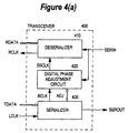
- Deserialization 304 is sensitive to the phase of the serial data stream on line SERIN. If the serial data stream is out-of-phase with respect to local clock signal LCLK, then it is possible that bit data of the serial data stream would be latched incorrectly. For example, if the serial data stream is out-of-phase by a bit period, then bit TDATA(0) would be incorrectly received as RDATA(1), TDATA(1) as RDATA(2), and so forth. Accordingly, one embodiment of the invention provides a high-speed, phase-independent transceiver, shown as transceiver 400 in Figure 4(a) and described in U.S. Patent No. 5,400,370 issued to Guo on March 21, 1995, incorporated herein by reference.
- Transceiver 400 is all-digital, in that it does not implement large, lumped, analog components, such as capacitors, for data storage, timing or other functions, and hence readily implemented upon a large scale integrated circuit.
- the transceiver 400 has three major components, deserializer 410 , digital phase adjustment circuit 420, and serializer 430 .
- Serializer 430 described in U.S. Patent No. 5,349,612, issued to Guo et al. on September 20, 1994, incorporated herein by reference, receives parallel data package TDATA, in N-bit nybbles clocked by local clock LCLK. The operation of serializer 430 in serializing an N-bit nybble TDATA is described with reference to the timing diagram in Fig. 4(b).
- serializer 430 For each cycle of local clock LCLK, serializer 430 generates N cycles of bit clock BCLK, the first bit clock cycle being aligned with an edge of local clock LCLK .
- the period of bit clock BCLK is at most the period of local clock LCLK divided by N, but the bit clock period does not have to be an integral fraction of the local clock period.
- the cycles of bit clock BCLK are produced by a cascade of adjustable, digital delay elements, which are preferably calibrated by an on-chip digital servo subcomponent of serializer 430, described in U.S. Patent No. 5,457,719, issued to Guo et al. on October 10, 1995.
- the result of the calibration circuit is sent as signal ADJ from serializer 430 to also calibrate the adjustable, digital delay elements of digital phase adjustment circuit 420.
- serializer 430 encodes nybble TDATA into a bit stream SEROUT, which may be an ECL signal for high-speed transmission.
- One encoding, as shown in Fig. 4(b) is NRZI (Non-Return to Zero, Invert on one), where a transition signifies a one and a lack of a transition signifies a zero.
- NRZI Non-Return to Zero, Invert on one
- Other encodings such as NRZ or Manchester may be used as well in other embodiments of the invention.
- transceiver 400 When transceiver 400 receives an incoming serial data stream SERIN, the clock signal for incoming serial data stream SERIN is generally out of phase with respect to bit clock BCLK. Therefore, digital phase adjustment circuit 420 shifts the phase of the bit clock BCLK to create shifted bit clock SBCLK, having a timing edge aligned with the center of the data eye of the incoming serial data stream SERIN.
- Deserializer 410 takes shifted bit clock SBCLK and decodes incoming serial data stream SERIN, into received data nybble RDATA. Deserializer 410 is described in more detail in U.S. Patent No. 5,367,542, issued to Guo on November 22, 1994, incorporated herein by reference.
Landscapes
- Engineering & Computer Science (AREA)
- Power Engineering (AREA)
- Computer Networks & Wireless Communication (AREA)
- Signal Processing (AREA)
- Logic Circuits (AREA)
- Dc Digital Transmission (AREA)
- Semiconductor Integrated Circuits (AREA)
Applications Claiming Priority (2)
| Application Number | Priority Date | Filing Date | Title |
|---|---|---|---|
| US962667 | 1997-11-03 | ||
| US08/962,667 US6192069B1 (en) | 1997-11-03 | 1997-11-03 | Circuit and methodology for transferring signals between semiconductor devices |
Publications (2)
| Publication Number | Publication Date |
|---|---|
| EP0913954A2 true EP0913954A2 (fr) | 1999-05-06 |
| EP0913954A3 EP0913954A3 (fr) | 2003-09-17 |
Family
ID=25506201
Family Applications (1)
| Application Number | Title | Priority Date | Filing Date |
|---|---|---|---|
| EP98304051A Withdrawn EP0913954A3 (fr) | 1997-11-03 | 1998-05-21 | Circuit et méthode pour le transfert de signaux entre des dispositifs semiconducteurs |
Country Status (3)
| Country | Link |
|---|---|
| US (1) | US6192069B1 (fr) |
| EP (1) | EP0913954A3 (fr) |
| JP (1) | JPH11177406A (fr) |
Cited By (3)
| Publication number | Priority date | Publication date | Assignee | Title |
|---|---|---|---|---|
| WO2001031410A1 (fr) * | 1999-10-29 | 2001-05-03 | Regis Munoz | Systeme de traitement de fils |
| EP1487128A1 (fr) | 2003-06-11 | 2004-12-15 | The Boeing Company | Transmissions numériques sur lignes d'alimentation à 28 V DC |
| US11323435B2 (en) | 2019-05-08 | 2022-05-03 | The Boeing Company | Method and apparatus for advanced security systems over a power line connection |
Families Citing this family (11)
| Publication number | Priority date | Publication date | Assignee | Title |
|---|---|---|---|---|
| DE10019811A1 (de) * | 2000-04-20 | 2001-10-31 | Infineon Technologies Ag | Integrierte Schaltung |
| US7231008B2 (en) * | 2002-11-15 | 2007-06-12 | Vitesse Semiconductor Corporation | Fast locking clock and data recovery unit |
| US7286572B2 (en) * | 2003-01-10 | 2007-10-23 | Sierra Monolithics, Inc. | Highly integrated, high-speed, low-power serdes and systems |
| FR2937199B1 (fr) * | 2008-10-13 | 2016-01-22 | Sagem Defense Securite | Systeme avionique comprenant un control relie a un peripherique par une ligne mutualisee pour la puissance et les donnees. |
| FR2937200A1 (fr) * | 2008-10-13 | 2010-04-16 | Sagem Defense Securite | Systeme avionique comprenant un controleur et au moins un peripherique relies par une ligne mutualisee pour la puissance et les donnees |
| US8483344B2 (en) | 2011-06-13 | 2013-07-09 | Stephen C. Dillinger | Fast lock serializer-deserializer (SERDES) architecture |
| US9577818B2 (en) * | 2015-02-04 | 2017-02-21 | Teradyne, Inc. | High speed data transfer using calibrated, single-clock source synchronous serializer-deserializer protocol |
| FR3083940A1 (fr) | 2018-07-13 | 2020-01-17 | Zodiac Aerotechnics | Dispositif d'emission et de transmission de donnees et dispositif de transmission et de reception de donnees |
| FR3083939A1 (fr) | 2018-07-13 | 2020-01-17 | Zodiac Aerotechnics | Systeme de transmission de donnees |
| WO2019193291A1 (fr) * | 2018-04-04 | 2019-10-10 | Zodiac Aerotechnics | Dispositif d'émission de données, dispositif de réception de données et système de transmission de données |
| WO2019193292A1 (fr) * | 2018-04-04 | 2019-10-10 | Zodiac Aerotechnics | Système de transmission de données |
Family Cites Families (17)
| Publication number | Priority date | Publication date | Assignee | Title |
|---|---|---|---|---|
| JPS6044854B2 (ja) * | 1980-04-22 | 1985-10-05 | 岩崎通信機株式会社 | 信号伝送方式 |
| US4631361A (en) * | 1984-06-28 | 1986-12-23 | Itt Corporation | Programmable ring generator |
| US5132572A (en) | 1991-08-12 | 1992-07-21 | Advanced Micro Devices, Inc. | High-speed CMOS-to-ECL translator circuit |
| US5227679A (en) | 1992-01-02 | 1993-07-13 | Advanced Micro Devices, Inc. | Cmos digital-controlled delay gate |
| US5220216A (en) | 1992-01-02 | 1993-06-15 | Woo Ann K | Programmable driving power of a CMOS gate |
| US5363419A (en) | 1992-04-24 | 1994-11-08 | Advanced Micro Devices, Inc. | Dual phase-locked-loop having forced mid range fine control zero at handover |
| US5349612A (en) * | 1992-06-19 | 1994-09-20 | Advanced Micro Devices, Inc. | Digital serializer and time delay regulator |
| US5367542A (en) | 1992-06-19 | 1994-11-22 | Advanced Micro Devices, Inc. | Digital data recovery using delay time rulers |
| US5452333A (en) | 1992-06-19 | 1995-09-19 | Advanced Micro Devices, Inc. | Digital jitter correction method and signal preconditioner |
| US5264745A (en) | 1992-08-28 | 1993-11-23 | Advanced Micro Devices, Inc. | Recovering phase and data from distorted duty cycles caused by ECL-to-CMOS translator |
| US5400370A (en) | 1993-02-24 | 1995-03-21 | Advanced Micro Devices Inc. | All digital high speed algorithmic data recovery method and apparatus using locally generated compensated broad band time rulers and data edge position averaging |
| US5457719A (en) | 1993-08-11 | 1995-10-10 | Advanced Micro Devices Inc. | All digital on-the-fly time delay calibrator |
| ATE226769T1 (de) * | 1993-10-22 | 2002-11-15 | Valtac Alex Beaud | Übertragungssystem |
| JPH07273695A (ja) * | 1994-01-24 | 1995-10-20 | Yair Maryanka | 直流導線を介する音声、音楽、映像、データの伝送 |
| US5457336A (en) | 1994-10-13 | 1995-10-10 | Advanced Micro Devices, Inc. | Non-volatile memory structure including protection and structure for maintaining threshold stability |
| US5818821A (en) * | 1994-12-30 | 1998-10-06 | Intelogis, Inc. | Universal lan power line carrier repeater system and method |
| US5886539A (en) * | 1997-04-10 | 1999-03-23 | Advanced Micro Devices, Ind | Communication within an integrated circuit by data serialization through a metal plane |
-
1997
- 1997-11-03 US US08/962,667 patent/US6192069B1/en not_active Expired - Lifetime
-
1998
- 1998-05-21 EP EP98304051A patent/EP0913954A3/fr not_active Withdrawn
- 1998-06-15 JP JP10166863A patent/JPH11177406A/ja not_active Withdrawn
Cited By (5)
| Publication number | Priority date | Publication date | Assignee | Title |
|---|---|---|---|---|
| WO2001031410A1 (fr) * | 1999-10-29 | 2001-05-03 | Regis Munoz | Systeme de traitement de fils |
| US6705131B1 (en) | 1999-10-29 | 2004-03-16 | Regis Munoz | Yarn processing system |
| EP1487128A1 (fr) | 2003-06-11 | 2004-12-15 | The Boeing Company | Transmissions numériques sur lignes d'alimentation à 28 V DC |
| US6995658B2 (en) | 2003-06-11 | 2006-02-07 | The Boeing Company | Digital communication over 28VDC power line |
| US11323435B2 (en) | 2019-05-08 | 2022-05-03 | The Boeing Company | Method and apparatus for advanced security systems over a power line connection |
Also Published As
| Publication number | Publication date |
|---|---|
| EP0913954A3 (fr) | 2003-09-17 |
| JPH11177406A (ja) | 1999-07-02 |
| US6192069B1 (en) | 2001-02-20 |
Similar Documents
| Publication | Publication Date | Title |
|---|---|---|
| US6192069B1 (en) | Circuit and methodology for transferring signals between semiconductor devices | |
| US5384808A (en) | Method and apparatus for transmitting NRZ data signals across an isolation barrier disposed in an interface between adjacent devices on a bus | |
| US7737871B2 (en) | MCU with integrated voltage isolator to provide a galvanic isolation between input and output | |
| US6297684B1 (en) | Circuit and method for switching between digital signals that have different signal rates | |
| CN100452787C (zh) | 检测进入信号从一种已知的先前逻辑状态转变的方法 | |
| US6157206A (en) | On-chip termination | |
| US4761567A (en) | Clock scheme for VLSI systems | |
| US6721379B1 (en) | DAC/Driver waveform generator with phase lock rise time control | |
| US6249164B1 (en) | Delay circuit arrangement for use in a DAC/driver waveform generator with phase lock rise time control | |
| US6417790B1 (en) | Low-power data serializer | |
| EP3723291A1 (fr) | Circuit de transmetteur doté d'un circuit d'attaque de pré-emphase | |
| EP3734465B1 (fr) | Code et interface de transmission de données | |
| US6232796B1 (en) | Apparatus and method for detecting two data bits per clock edge | |
| US12028057B2 (en) | Receivers for high density and low latency chip-to-chip links | |
| CN121257448B (zh) | Ddr输出驱动器电路和ddr芯片 | |
| WO1998045787A1 (fr) | Reduction du nombre de broches par des techniques de serialisation | |
| US6384642B1 (en) | Switched positive feedback for controlled receiver impedance | |
| KR100210394B1 (ko) | 다치논리데이터송신시스템 | |
| CA2415289C (fr) | Methode et appareil de transmission de signaux de donnees nrz a travers une barriere isolante installee dans une interface montee entre disposi ifs adjacents sur un bus | |
| US20050265062A1 (en) | Chip to chip interface | |
| KR100202943B1 (ko) | 다치논리데이터송신시스템 | |
| US20050122135A1 (en) | Chip to chip interface | |
| JPH05243954A (ja) | 信号レベルの変換機能を備えた集積回路 | |
| GB2308516A (en) | Microprocessor interface circuit and system | |
| HK1052063B (en) | Method and apparatus for transmitting nrz data signals across an isolation barrier disposed in an interface between adjacent devices on a bus |
Legal Events
| Date | Code | Title | Description |
|---|---|---|---|
| PUAI | Public reference made under article 153(3) epc to a published international application that has entered the european phase |
Free format text: ORIGINAL CODE: 0009012 |
|
| AK | Designated contracting states |
Kind code of ref document: A2 Designated state(s): AT BE CH CY DE DK ES FI FR GB GR IE IT LI LU MC NL PT SE |
|
| AX | Request for extension of the european patent |
Free format text: AL;LT;LV;MK;RO;SI |
|
| PUAL | Search report despatched |
Free format text: ORIGINAL CODE: 0009013 |
|
| AK | Designated contracting states |
Kind code of ref document: A3 Designated state(s): AT BE CH CY DE DK ES FI FR GB GR IE IT LI LU MC NL PT SE |
|
| AX | Request for extension of the european patent |
Extension state: AL LT LV MK RO SI |
|
| RIC1 | Information provided on ipc code assigned before grant |
Ipc: 7H 04B 3/56 B Ipc: 7H 04B 3/54 A |
|
| STAA | Information on the status of an ep patent application or granted ep patent |
Free format text: STATUS: THE APPLICATION IS DEEMED TO BE WITHDRAWN |
|
| AKX | Designation fees paid | ||
| REG | Reference to a national code |
Ref country code: DE Ref legal event code: 8566 |
|
| 18D | Application deemed to be withdrawn |
Effective date: 20031202 |