EP0915424A2 - Datenpufferspeicher mit einem Aktualisierungsbefehl - Google Patents
Datenpufferspeicher mit einem Aktualisierungsbefehl Download PDFInfo
- Publication number
- EP0915424A2 EP0915424A2 EP98121206A EP98121206A EP0915424A2 EP 0915424 A2 EP0915424 A2 EP 0915424A2 EP 98121206 A EP98121206 A EP 98121206A EP 98121206 A EP98121206 A EP 98121206A EP 0915424 A2 EP0915424 A2 EP 0915424A2
- Authority
- EP
- European Patent Office
- Prior art keywords
- cache
- controller
- cache memory
- memory
- data
- Prior art date
- Legal status (The legal status is an assumption and is not a legal conclusion. Google has not performed a legal analysis and makes no representation as to the accuracy of the status listed.)
- Withdrawn
Links
Images

Classifications
-
- G—PHYSICS
- G06—COMPUTING OR CALCULATING; COUNTING
- G06F—ELECTRIC DIGITAL DATA PROCESSING
- G06F12/00—Accessing, addressing or allocating within memory systems or architectures
- G06F12/02—Addressing or allocation; Relocation
- G06F12/08—Addressing or allocation; Relocation in hierarchically structured memory systems, e.g. virtual memory systems
- G06F12/0802—Addressing of a memory level in which the access to the desired data or data block requires associative addressing means, e.g. caches
- G06F12/0862—Addressing of a memory level in which the access to the desired data or data block requires associative addressing means, e.g. caches with prefetch
-
- G—PHYSICS
- G06—COMPUTING OR CALCULATING; COUNTING
- G06F—ELECTRIC DIGITAL DATA PROCESSING
- G06F12/00—Accessing, addressing or allocating within memory systems or architectures
-
- G—PHYSICS
- G06—COMPUTING OR CALCULATING; COUNTING
- G06F—ELECTRIC DIGITAL DATA PROCESSING
- G06F12/00—Accessing, addressing or allocating within memory systems or architectures
- G06F12/02—Addressing or allocation; Relocation
- G06F12/08—Addressing or allocation; Relocation in hierarchically structured memory systems, e.g. virtual memory systems
- G06F12/0802—Addressing of a memory level in which the access to the desired data or data block requires associative addressing means, e.g. caches
- G06F12/0844—Multiple simultaneous or quasi-simultaneous cache accessing
- G06F12/0846—Cache with multiple tag or data arrays being simultaneously accessible
-
- G—PHYSICS
- G06—COMPUTING OR CALCULATING; COUNTING
- G06F—ELECTRIC DIGITAL DATA PROCESSING
- G06F12/00—Accessing, addressing or allocating within memory systems or architectures
- G06F12/02—Addressing or allocation; Relocation
- G06F12/08—Addressing or allocation; Relocation in hierarchically structured memory systems, e.g. virtual memory systems
- G06F12/10—Address translation
- G06F12/1027—Address translation using associative or pseudo-associative address translation means, e.g. translation look-aside buffer [TLB]
- G06F12/1045—Address translation using associative or pseudo-associative address translation means, e.g. translation look-aside buffer [TLB] associated with a data cache
-
- G—PHYSICS
- G06—COMPUTING OR CALCULATING; COUNTING
- G06F—ELECTRIC DIGITAL DATA PROCESSING
- G06F2212/00—Indexing scheme relating to accessing, addressing or allocation within memory systems or architectures
- G06F2212/60—Details of cache memory
- G06F2212/6028—Prefetching based on hints or prefetch instructions
Definitions
- the present invention relates to a cache memory system.
- hierarchically-structured cache memory has become popular to speed up access to memory.
- data to be accessed is not in the cache memory of a cache memory system, an attempt to get data from cache memory results in a miss hit and data is transferred from main memory to cache memory. Therefore, when desired data is not in cache memory, the processor must suspend its processing until the transfer of data from main memory to cache memory is finished, decreasing the processing capacity.
- Japanese Patent Publication Kokai JP-A No. Hei 4-190438 discloses a method in which a program execution flow is read ahead to bring data, which will be used at branch addresses, into cache memory in advance.
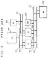
- FIG. 3 is a block diagram showing the configuration of conventional cache memory.
- a central processing unit CPU 301 is connected to cache memory CM 303 and to a cache controller CMC 304 via an address bus 311 and a data bus 321.
- a sub-processing unit SPU 302 is connected to the cache controller CMC 304 via an address bus 312 and the data bus 321, and to the cache memory CM 303 via the data bus 321.
- the sub-processing unit 302 monitors instructions to be sent to the central processing unit CPU 301 via the data bus 321.
- the sub-processing unit 302 tells the cache controller CMC 304 to update cache memory.
- the cache controller CMC 304 itself does not update cache memory; instead, the cache controller CMC 304 passes update address information to a DMA controller 305 and causes it to start transferring data from main memory 306 to a location in cache memory 303 indicated by the address information.
- This cache update instruction meaningless to the central processing unit CPU 301, is ignored. After that, when control is passed to the jump instruction, no hit miss occurs because data has already been sent from main memory 306 to cache memory CM 303.
- Another proposed method is that the sub-processing unit SPU 302 fetches an instruction which is several instructions ahead of the current instruction to find a miss hit in advance and to cause the cache controller CMC 304 to update cache memory.
- a general mechanism of cache memory is described, for example, in "Computer Configuration and Design” (Nikkei BP).
- the first problem is that the system according to the prior art requires hardware specifically designed to monitor programs, resulting in a large-sized circuit.
- the second problem is that reading an instruction that is several instructions ahead of the current instruction requires the memory to have two or more ports. Normally, memory with two or more ports is large.
- the third problem is that, because the update instruction is inserted automatically by a compiler into a location that is several instructions ahead of the current instruction, the cache memory update start time cannot be set freely. Therefore, even when it is found that it takes longer to update cache memory because of an increase in the cache memory block size or in the main memory access time, cache memory updating cannot be started at an earlier time. This sometimes results in cache memory updating not being completed within a predetermined period of time.
- the fourth problem is that the method of automatically inserting a jump instruction, through the use of a compiler, into a location several instructions ahead of the current instruction requires the compiler to have that function built-in, increasing the development cost of development tools such as a compiler.
- the present invention seeks to solve the problems associated with the prior art described above. It is an object of the present invention to provide a cache memory system which is based on the configuration of the configured main memory or cache memory and which updates cache memory efficiently without an additional compiler function or without a special device for monitoring instructions.
- the present invention provides a cache memory system comprising a memory composed of a plurality of banks, a cache controller sending a cache update instruction to a Direct Memory Access DMA controller as directed by a central processing unit, and the DMA controller which transfers data from main memory to cache memory according to the instruction received from said cache controller.
- a cache memory system comprises cache memory (3 in FIG. 1) which is composed of a plurality of banks and a cache controller (2 in FIG. 1) which sends a cache update instruction to a Direct Memory Access (DMA) controller (4 in FIG. 1) as directed by a central processing unit 1.
- the DMA controller 4 transfers data between a main memory (5 in FIG. 1) and the cache memory (3 in FIG. 1) in the DMA mode.
- the cache memory system according to the present invention is composed of a plurality of banks which may be accessed from different resources at the same time.
- the cache memory system allows data to be transferred between the memory bank and the main memory concurrently with the processing of the central processing unit 1 without stopping the processing of the central processing unit 1.
- the cache memory system coordinates access to the cache memory, i.e., coordinating access to the banks so as to allow the other bank (or any of other remaining banks) to be accessed.
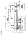
- FIG. 1 is a diagram showing the configuration of the example of the present invention.
- a microprocessor used in the example of the present invention comprises a central processing unit (CPU) 1, cache memory 3 connected to the central processing unit 1 via an address bus 11 and a data bus 12, a cache controller 2, a DMA controller 4, and main memory 5.
- CPU central processing unit
- cache memory 3 connected to the central processing unit 1 via an address bus 11 and a data bus 12, a cache controller 2, a DMA controller 4, and main memory 5.
- the cache memory 3 is connected to the DMA controller 4 via a DMA address bus 21 and a DMA data bus 22.
- signal line 24 activating the DMA controller 4 is sent from the cache controller 2 to the DMA controller 4.
- the DMA controller 4 is connected to main memory 5 via an external address bus 41 and an external data bus 42.
- a processing-stopping signal line 7 is connected from the cache controller 2 to the central processing unit 1.
- the cache controller 2 divides the cache memory 3 into a plurality of blocks, each composed of a number of words that are updated at a time.
- tag memory (not shown) is provided for managing the blocks.
- the tag memory contains a predetermined number of bits of the address of each of a block storing the contents in the cache memory 3.
- the tag portion of the address is stored in the tag memory to allow the corresponding block storing the contents in the cache memory 3 to be identified.
- the cache controller 2 also has a command register into which a cache update instruction from the central processing unit 1 is stored. When it is detected that a cache miss occurs or that data is written into the command register, a DMA transfer instruction is issued to the DMA controller 4.
- the cache memory 3 composed of a plurality of banks, is faster in speed than the main memory 5.
- Multiplexers 61, 62, 63, and 64 are connected to the cache memory 3 to allow each bank to select a device to or from which data is sent.
- the number of banks is not limited to two although only two banks are shown in FIG. 1.
- the DMA controller 4 starts operation upon receiving an instruction from the cache controller 2. At this time, the DMA controller 4 receives information on source data (the start address of the source data in the main memory 5 and the number of words of the source data) and information on a destination location (the start address of the destination location in the cache memory 3 to which the data is to be sent).
- source data the start address of the source data in the main memory 5 and the number of words of the source data
- destination location the start address of the destination location in the cache memory 3 to which the data is to be sent.
- the DMA controller 4 sends data directly to the cache memory 3, not via the central processing unit 1 or the cache controller 2.
- FIG. 2 shows an example of the command register in the cache controller 2.
- the command register is composed of a cache update start address field and a number-of-blocks field.
- the central processing unit 1 when the central processing unit 1 reads data, it sends an address to the cache controller 2 and the cache memory 3 via the address bus 11.
- the cache controller 2 gets a portion of the address from the central processing unit 1 and references the tag memory to determine whether desired data is in the cache memory 3.
- the central processing unit 1 When desired data is found, the central processing unit 1 reads it from the cache memory 3. On the other hand, when desired data is not in the cache memory 3, the cache controller 2 stops the processing of the central processing unit 1, updates the tag memory, sends cache memory update information (the start address of the block containing desired data, the number of words to be transferred, and the start address in cache memory at which data is to be sent) to the DMA controller 4, and tells it to update the cache memory 3.
- cache memory update information the start address of the block containing desired data, the number of words to be transferred, and the start address in cache memory at which data is to be sent
- the DMA controller 4 Upon receiving the instruction from the cache controller 2, the DMA controller 4 transfers data from the main memory 5 to the cache memory 3.
- the cache controller 2 resumes the processing of the central processing unit 1.
- the central processing unit 1 executes a command data transfer instruction.
- This instruction a user-coded instruction embedded among other instructions, sends command data to the command register which is mapped into memory from the cache controller 2.
- the cache controller 2 generates the block start address from the start address data in the command register; it also generates the number of transfer words from the number-of-blocks data in the command register. Then, as in the usual cache-fill operation, the cache controller 2 sends to the DMA controller 4 the start address of the block to be loaded and the number of words to be transferred as well as the start address of the corresponding block within the cache memory to which data is to be sent.
- the cache memory 3 is updated.
- the multiplexers 63 and 64 which have been connected to the central processing unit 1, are turned to connect to the DMA controller 4 to receive data for the bank in the cache memory 3 to which data is to be sent.
- the cache controller 2 changes the content of the internal tag memory to the tag corresponding to the block to be updated. This transfer, which is performed between the cache controller 2 and the DMA controller 4, does not affect the central processing unit 1.
- the transfer may be done concurrently with processing of the central processing unit 1, whereupon the central processing unit 1 need not be stopped.
- the bank in the cache memory 3 to be updated is being used by the central processing unit 1, access from the central processing unit 1 and from the DMA controller 4 must be coordinated.
- Access coordination is done, for example, by keeping the processing-stop signal to the central processing unit 1 asserted until the cache memory is updated. This method ensures that the program will be completed without failure although the central processing unit 1 may be placed in the stopped state for a prolonged time depending upon the time at which the update instruction is issued.
- Another coordination method prevents the DMA controller 4 from accessing the cache memory until the central processing unit 1 ends processing.
- the cache system according to the present invention has the following advantages.
- the first advantage of the present invention is that the cache system does not require a special device for monitoring programs, reducing the size of the circuit.
- the second advantage of the present invention is that the cache system prevents the hardware size from increasing. This is because the cache system does not use memory with two or more ports.
- the third advantage of the present invention is that the update start time of cache memory may be set freely.
- the command data transfer instruction may be specified early enough for cache memory updating to be completed.
- the fourth advantage of the present invention is that the cache system does not require an additional compiler and therefore does not require additional development costs.
Landscapes
- Engineering & Computer Science (AREA)
- Theoretical Computer Science (AREA)
- Physics & Mathematics (AREA)
- General Engineering & Computer Science (AREA)
- General Physics & Mathematics (AREA)
- Memory System Of A Hierarchy Structure (AREA)
Applications Claiming Priority (3)
| Application Number | Priority Date | Filing Date | Title |
|---|---|---|---|
| JP32206897A JP3289661B2 (ja) | 1997-11-07 | 1997-11-07 | キャッシュメモリシステム |
| JP32206897 | 1997-11-07 | ||
| JP322068/97 | 1997-11-07 |
Publications (2)
| Publication Number | Publication Date |
|---|---|
| EP0915424A2 true EP0915424A2 (de) | 1999-05-12 |
| EP0915424A3 EP0915424A3 (de) | 2000-10-04 |
Family
ID=18139567
Family Applications (1)
| Application Number | Title | Priority Date | Filing Date |
|---|---|---|---|
| EP98121206A Withdrawn EP0915424A3 (de) | 1997-11-07 | 1998-11-06 | Datenpufferspeicher mit einem Aktualisierungsbefehl |
Country Status (6)
| Country | Link |
|---|---|
| US (1) | US6219759B1 (de) |
| EP (1) | EP0915424A3 (de) |
| JP (1) | JP3289661B2 (de) |
| KR (1) | KR100327854B1 (de) |
| CN (1) | CN1125401C (de) |
| TW (1) | TW390986B (de) |
Cited By (2)
| Publication number | Priority date | Publication date | Assignee | Title |
|---|---|---|---|---|
| WO2014201961A1 (en) * | 2013-06-20 | 2014-12-24 | Silicon Motion, Inc. | Control device and access system utilizing the same |
| US9898302B2 (en) | 2013-06-20 | 2018-02-20 | Silicon Motion, Inc. | Control device and access system utilizing the same |
Families Citing this family (30)
| Publication number | Priority date | Publication date | Assignee | Title |
|---|---|---|---|---|
| KR19990049284A (ko) * | 1997-12-12 | 1999-07-05 | 구본준 | 데이터 프로그램 장치 |
| US6434649B1 (en) * | 1998-10-14 | 2002-08-13 | Hitachi, Ltd. | Data streamer |
| US6560674B1 (en) | 1998-10-14 | 2003-05-06 | Hitachi, Ltd. | Data cache system |
| US6574682B1 (en) * | 1999-11-23 | 2003-06-03 | Zilog, Inc. | Data flow enhancement for processor architectures with cache |
| US6859862B1 (en) * | 2000-04-07 | 2005-02-22 | Nintendo Co., Ltd. | Method and apparatus for software management of on-chip cache |
| JP2001344153A (ja) | 2000-05-30 | 2001-12-14 | Nec Corp | マルチプロセッサシステムのキャッシュメモリ制御装置 |
| EP1182561B1 (de) * | 2000-08-21 | 2011-10-05 | Texas Instruments France | Cache-Speicher mit Blockvorausholung und DMA |
| US6799264B2 (en) * | 2001-02-20 | 2004-09-28 | Koninklijke Philips Electronics N.V. | Memory accelerator for ARM processor pre-fetching multiple instructions from cyclically sequential memory partitions |
| US6754733B2 (en) * | 2001-08-23 | 2004-06-22 | Texas Instruments Incorporated | Shared memory architecture for increased bandwidth in a printer controller |
| KR100541366B1 (ko) * | 2002-07-19 | 2006-01-16 | 주식회사 하이닉스반도체 | 고속 데이터 억세스를 위한 디램 |
| JP4837247B2 (ja) * | 2003-09-24 | 2011-12-14 | パナソニック株式会社 | プロセッサ |
| CN100390755C (zh) * | 2003-10-14 | 2008-05-28 | 中国科学院计算技术研究所 | 含有显式高速缓冲存储器的计算机微体系结构 |
| CN1308840C (zh) * | 2004-02-13 | 2007-04-04 | 联想(北京)有限公司 | 一种获取硬盘中数据的方法 |
| US7769950B2 (en) | 2004-03-24 | 2010-08-03 | Qualcomm Incorporated | Cached memory system and cache controller for embedded digital signal processor |
| US7657667B2 (en) * | 2004-03-25 | 2010-02-02 | International Business Machines Corporation | Method to provide cache management commands for a DMA controller |
| JP4451717B2 (ja) | 2004-05-31 | 2010-04-14 | 株式会社ソニー・コンピュータエンタテインメント | 情報処理装置および情報処理方法 |
| US7669009B2 (en) * | 2004-09-23 | 2010-02-23 | Intel Corporation | Method and apparatus for run-ahead victim selection to reduce undesirable replacement behavior in inclusive caches |
| US8065459B2 (en) * | 2006-05-17 | 2011-11-22 | Nxp B.V. | Multi-processing system and a method of executing a plurality of data processing tasks |
| JP2008090492A (ja) * | 2006-09-29 | 2008-04-17 | Fujitsu Ltd | キャッシュコントローラ、マイクロプロセッサシステム、記憶装置 |
| US7721066B2 (en) | 2007-06-05 | 2010-05-18 | Apple Inc. | Efficient encoding for detecting load dependency on store with misalignment |
| US20110004732A1 (en) * | 2007-06-06 | 2011-01-06 | 3Leaf Networks, Inc. | DMA in Distributed Shared Memory System |
| US8166213B2 (en) * | 2007-11-21 | 2012-04-24 | Microchip Technology Incorporated | Controller with indirect accessible memory |
| US8069300B2 (en) * | 2008-09-30 | 2011-11-29 | Micron Technology, Inc. | Solid state storage device controller with expansion mode |
| US8412862B2 (en) * | 2008-12-18 | 2013-04-02 | International Business Machines Corporation | Direct memory access transfer efficiency |
| US8352646B2 (en) * | 2010-12-16 | 2013-01-08 | International Business Machines Corporation | Direct access to cache memory |
| CN102955872B (zh) * | 2011-08-31 | 2016-05-04 | 北京中电华大电子设计有限责任公司 | 具有参数传递功能的仿真器 |
| US9098491B2 (en) * | 2012-11-23 | 2015-08-04 | Hong Kong Applied Science and Technology Research Institute Company Limited | Method and system for performing data transfer with a flash storage medium |
| US9239788B2 (en) * | 2013-10-24 | 2016-01-19 | Qualcomm Incorporated | Split write operation for resistive memory cache |
| CN105786733B (zh) * | 2014-12-26 | 2020-08-07 | 南京中兴新软件有限责任公司 | 一种写入tcam条目的方法及装置 |
| US11048636B2 (en) * | 2019-07-31 | 2021-06-29 | Micron Technology, Inc. | Cache with set associativity having data defined cache sets |
Family Cites Families (9)
| Publication number | Priority date | Publication date | Assignee | Title |
|---|---|---|---|---|
| JPS60258660A (ja) * | 1984-06-05 | 1985-12-20 | Fujitsu Ltd | キヤシユメモリ制御方式 |
| US5276852A (en) * | 1990-10-01 | 1994-01-04 | Digital Equipment Corporation | Method and apparatus for controlling a processor bus used by multiple processor components during writeback cache transactions |
| JPH04190438A (ja) | 1990-11-26 | 1992-07-08 | Hitachi Ltd | ディジタル処理システム |
| WO1994023374A2 (en) * | 1993-03-30 | 1994-10-13 | Ast Research Inc | STROBOSCOPIC LOGIC FOR TRIGGERING SIMULATED BUS CONTROL CYCLES |
| JPH10509819A (ja) * | 1994-10-14 | 1998-09-22 | シリコン グラフィックス インク. | インターリーブされるキャッシュメモリアレイのインデッキシングとマルチプレキシング |
| JPH08263424A (ja) * | 1995-03-20 | 1996-10-11 | Fujitsu Ltd | コンピュータ装置 |
| US5838943A (en) * | 1996-03-26 | 1998-11-17 | Advanced Micro Devices, Inc. | Apparatus for speculatively storing and restoring data to a cache memory |
| US5802569A (en) * | 1996-04-22 | 1998-09-01 | International Business Machines Corp. | Computer system having cache prefetching amount based on CPU request types |
| US6012106A (en) * | 1997-11-03 | 2000-01-04 | Digital Equipment Corporation | Prefetch management for DMA read transactions depending upon past history of actual transfer lengths |
-
1997
- 1997-11-07 JP JP32206897A patent/JP3289661B2/ja not_active Expired - Fee Related
-
1998
- 1998-10-19 TW TW087117286A patent/TW390986B/zh not_active IP Right Cessation
- 1998-11-06 EP EP98121206A patent/EP0915424A3/de not_active Withdrawn
- 1998-11-06 US US09/187,486 patent/US6219759B1/en not_active Expired - Lifetime
- 1998-11-06 CN CN98123593A patent/CN1125401C/zh not_active Expired - Fee Related
- 1998-11-06 KR KR1019980047422A patent/KR100327854B1/ko not_active Expired - Fee Related
Cited By (2)
| Publication number | Priority date | Publication date | Assignee | Title |
|---|---|---|---|---|
| WO2014201961A1 (en) * | 2013-06-20 | 2014-12-24 | Silicon Motion, Inc. | Control device and access system utilizing the same |
| US9898302B2 (en) | 2013-06-20 | 2018-02-20 | Silicon Motion, Inc. | Control device and access system utilizing the same |
Also Published As
| Publication number | Publication date |
|---|---|
| CN1217506A (zh) | 1999-05-26 |
| KR100327854B1 (ko) | 2002-08-13 |
| KR19990045059A (ko) | 1999-06-25 |
| EP0915424A3 (de) | 2000-10-04 |
| JP3289661B2 (ja) | 2002-06-10 |
| CN1125401C (zh) | 2003-10-22 |
| JPH11143775A (ja) | 1999-05-28 |
| TW390986B (en) | 2000-05-21 |
| US6219759B1 (en) | 2001-04-17 |
Similar Documents
| Publication | Publication Date | Title |
|---|---|---|
| US6219759B1 (en) | Cache memory system | |
| US6671779B2 (en) | Management of caches in a data processing apparatus | |
| JPH05216687A (ja) | 割り込み中のキャッシュ動作を制御する方法および装置 | |
| US20020116581A1 (en) | Memory aliasing in a processor system | |
| JP2509344B2 (ja) | デ―タ処理装置 | |
| US5142671A (en) | Plural cache architecture for real time multitasking | |
| KR900007135B1 (ko) | 우선 선택회로를 갖는 바퍼 스토리지 제어 시스템 | |
| US7191319B1 (en) | System and method for preloading cache memory in response to an occurrence of a context switch | |
| JPH0895863A (ja) | コンピュータシステム、キャッシュヒットの判定方法 | |
| US7577791B2 (en) | Virtualized load buffers | |
| CA1299767C (en) | Cache memory control system | |
| US5513353A (en) | Cache control system which permanently inhibits local but not global parameter data writes to main memory | |
| US5201052A (en) | System for transferring first and second ring information from program status word register and store buffer | |
| JPH0784879A (ja) | キャッシュメモリ装置 | |
| EP0631236B1 (de) | Bus-Master-Rechnersystem und Verfahren | |
| JP3162459B2 (ja) | データ処理装置 | |
| JP3039391B2 (ja) | メモリシステム | |
| US7840757B2 (en) | Method and apparatus for providing high speed memory for a processing unit | |
| JPH1055308A (ja) | キャッシュメモリ | |
| JPH06124235A (ja) | キャッシュ制御方式 | |
| EP0376253A2 (de) | Informationsverarbeitungsvorrichtung mit Cache-Speicher | |
| JP2557857B2 (ja) | キヤツシユ記憶装置 | |
| US6564303B1 (en) | Dual port memory for digital signal processor | |
| JPH0713865A (ja) | キャッシュメモリ制御システム | |
| JPH05265916A (ja) | データ処理装置 |
Legal Events
| Date | Code | Title | Description |
|---|---|---|---|
| PUAI | Public reference made under article 153(3) epc to a published international application that has entered the european phase |
Free format text: ORIGINAL CODE: 0009012 |
|
| AK | Designated contracting states |
Kind code of ref document: A2 Designated state(s): DE FR GB |
|
| AX | Request for extension of the european patent |
Free format text: AL;LT;LV;MK;RO;SI |
|
| PUAL | Search report despatched |
Free format text: ORIGINAL CODE: 0009013 |
|
| AK | Designated contracting states |
Kind code of ref document: A3 Designated state(s): AT BE CH CY DE DK ES FI FR GB GR IE IT LI LU MC NL PT SE |
|
| AX | Request for extension of the european patent |
Free format text: AL;LT;LV;MK;RO;SI |
|
| 17P | Request for examination filed |
Effective date: 20010122 |
|
| AKX | Designation fees paid |
Free format text: DE FR GB |
|
| 17Q | First examination report despatched |
Effective date: 20020712 |
|
| STAA | Information on the status of an ep patent application or granted ep patent |
Free format text: STATUS: THE APPLICATION IS DEEMED TO BE WITHDRAWN |
|
| 18D | Application deemed to be withdrawn |
Effective date: 20030123 |