EP0915499B1 - Support pour plaquette semiconductrice - Google Patents
Support pour plaquette semiconductrice Download PDFInfo
- Publication number
- EP0915499B1 EP0915499B1 EP98120148A EP98120148A EP0915499B1 EP 0915499 B1 EP0915499 B1 EP 0915499B1 EP 98120148 A EP98120148 A EP 98120148A EP 98120148 A EP98120148 A EP 98120148A EP 0915499 B1 EP0915499 B1 EP 0915499B1
- Authority
- EP
- European Patent Office
- Prior art keywords
- temperature
- semiconductor wafer
- wafer
- temperature control
- wafer holding
- Prior art date
- Legal status (The legal status is an assumption and is not a legal conclusion. Google has not performed a legal analysis and makes no representation as to the accuracy of the status listed.)
- Expired - Lifetime
Links
Images





Classifications
-
- H—ELECTRICITY
- H10—SEMICONDUCTOR DEVICES; ELECTRIC SOLID-STATE DEVICES NOT OTHERWISE PROVIDED FOR
- H10P—GENERIC PROCESSES OR APPARATUS FOR THE MANUFACTURE OR TREATMENT OF DEVICES COVERED BY CLASS H10
- H10P72/00—Handling or holding of wafers, substrates or devices during manufacture or treatment thereof
- H10P72/06—Apparatus for monitoring, sorting, marking, testing or measuring
- H10P72/0602—Temperature monitoring
Definitions
- This invention relates to a semiconductor wafer holding apparatus, and more particularly to a semiconductor wafer holding apparatus applied to an electrical characteristic test unit and reliability test unit for semiconductors (hereinafter, referred to as chips) formed on a semiconductor wafer (hereinafter, referred to as a wafer).
- the invention relates to a semiconductor wafer storage chamber which houses a semiconductor wafer holding apparatus.
- the process of manufacturing semiconductors requires the technique for transferring wafers from one manufacturing process to another.
- the technique has been used in a mechanism for transferring wafers in units of carrier and in a mechanism for transferring wafers one by one.
- the number of the steps of processing wafers with larger diameters one by one, or the number of sheet-feeding processes has been increased, the number of the processes of transferring wafers one by one has been increased.
- the processes of manufacturing semiconductors include various testing processes. For instance, an electrical characteristic test unit checks a large number of chips formed on a semiconductor wafer for electrical characteristics. On the basis of the result of the test, screening is effected to obtain acceptable chips with the nondefective electrical characteristic. In the assembly process, the screened acceptable chips are packaged with synthetic resin or ceramic.
- a reliability test unit checks packaged products for potential defects in the chips by applying temperature and electrical stresses. On the basis of the result of the test, defective products are removed.
- a probing apparatus may be used for a reliability test.
- wafers have to be checked one by one and a lot of time is needed to test one wafer. Therefore, the reliability test using the probing apparatus has a cost problem.
- various difficult problems including an electrical connection between bare chips and sockets must be solved. The way of handling small bare chips is very complicated, which can lead to an increase in testing cost.
- the technique for causing a contactor to make in-unison contact with the chips on a wafer gives rise to problems with not only the relationship between the contactor and the wafer but also the relationship between the contactor and the construction of the wafer storage chamber.
- the inventors of the present invention have developed the technique for forming a contactor separately form a wafer storage chamber and causing the contactor to make in-unison contact with a wafer outside the wafer storage chamber and the technique for providing pogo pins to connect the contactor to the electric wiring (the junction terminals) in the wafer storage chamber.
- the electrical connection technique using pogo pins has the disadvantage that temperature rise during a test prevents the pogo pins from coming into contact with the contactors stably.
- An object of the present invention is to provide a wafer holding apparatus capable of measuring the temperature of a wafer accurately in an electrical characteristic test and reliability test for chips and improving the reliability of test.
- Another object of the present invention is to provide a wafer holding apparatus including a wafer holding table suitable to cause a contactor to make in-unison contact with the chips on a wafer.
- Another object of the present invention is to provide a highly reliable wafer holding apparatus capable of causing a contactor to come into contact with the junction terminals in a wafer storage chamber stably even during an inspection or a test.
- the second elastic support member should be coil-like springs wound around the rods.
- control unit for controlling the amount of heating by the heating element and the amount of cooling by the refrigerant should be a PID adjuster.
- the refrigerant should be water.
- the seal film should be made of silicone rubber and be in the form of a cylinder whose tip is sealed and whose bottom end is open.
- the support plate should be made of synthetic resin.
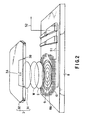
- a wafer storage chamber 1 in an embodiment of the present invention is in the form of a flat rectangle as a whole as shown in FIG. 1 .
- Many rows and columns of wafer storage chambers 1 are arranged horizontally in a frame (not shown) of, for example, a rack-like reliability test unit.
- a wafer W is integrated with a contactor 3 into a single entity on a wafer holding table (hereinafter, referred to as a wafer chuck) 2.
- a wafer holding table hereinafter, referred to as a wafer chuck
- each wafer W is put in each wafer storage chamber 1.
- the state where the wafer W has been integrated with the contactor 3 means a state where the test electrodes (hereinafter, referred to as electrode pads) of many chips formed on the top surface of the wafer W make in-unison contact with the test terminals 3A on the contactor 3 respectively, thereby connecting the electrode pads to the test terminals electrically.
- a structure where the wafer W, wafer chuck 2, and contactor have been integrated into an entity and these are referred to as a shell 4.
- the wafer storage chamber 1 is composed of a temperature control compartment 1A and a connector compartment 1B adjacent to the temperature control compartment 1A. Between the compartments 1A and 1B, a heat insulation wall (not shown) is provided. The heat insulation wall prevents the rise of the temperature in the connector compartment 1B as much as possible.
- the temperature control compartment 1A the temperature of the wafer W is kept at a test temperature and the temperate around the wafer W is forced to rise as little as possible.
- a base 5 is provided in the temperature control compartment 1A. In the four corners of the base 5, cylinder mechanisms 6 are provided. The top ends of the cylinder rods of the respective cylinder mechanisms 6 are coupled with the four corners of a pressure plate 7 provided above the base 5. On the back of the pressure plate 7, a clamp mechanism (not shown) is provided. The clamp mechanism receives a shell 4.
- a connector connected to a tester (not shown) and a wiring board connected to the connector are provided.
- a support plate 8 is provided in parallel with the base 5.
- a circular hole 8A is made in the middle of the support plate 8.
- a temperature control mechanism whose diameter is a little smaller than that of the hole 8A is provided as a bottom jacket 9 on the base.
- a large number of junction terminals (e.g., pogo pins or bump terminals) 10 e.g., 2000 to 3000 junction terminals
- junction terminals 10 are provided in such a manner that they correspond to a large number of external terminals (hereinafter, referred to as connection pads) arranged around the electrode pads 3A of the contactor 3 so as to form concentric circles. When the contactor comes into contact with the wafer W, the junction terminals 10 electrically connect to the connection pads 3B.
- the shell 4 transferred by the transfer mechanism (not shown) is received by the clamp mechanism in the temperature control compartment 1A.
- the cylinder mechanisms 6 force the pressure plate 7 to go down until the shell 4 has reached the bottom jacket 9.
- the back of the wafer chuck 2 for the shell 4 comes into contact with the top surface of the bottom jacket 9 and the connection pads 3B of the contactor 3 electrically connect to the pogo pins 10.
- the bottom jacket 9 controls the temperature of the wafer chuck 2 to keep the temperature of the wafer W at a specific test temperature (e.g., 110°C).
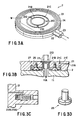
- the wafer chuck 2 is provided with a disk-like chuck body 21 as shown in FIGS. 3A and 3B .
- the chuck body 21 has a structure that is integrated with the contactor 3, while the body 21 is holding the wafer W.
- a gas flow path 21A is formed as shown in FIG. 3B .
- a gas supply pipe 22 is connected to the inlet (an opening in the peripheral surface of the body) of the gas flow path 21A.
- a gas exhaust pipe 23 is connected to the outlet (an opening adjacent to the inlet in the peripheral surface of the body) of the gas flow path 21A.
- a specific gas (chemically inactive gas, for example, nitrogen gas) is supplied and exhausted through the pipes 22, 23.
- ringed grooves 21B, 21C are made concentrically in the top surface of the chuck body 21. (In the figures, only two ringed grooves are shown). In these ringed grooves 21B, 21C, openings 21E leading to the gas flow path 21A are made in plural places.
- the contactor 3 When the contactor 3 has been laid on top of the wafer chuck 2, the air between the contactor 3 and chuck 2 is exhausted through the gas exhaust pipe 23 and then a low-pressure inert gas is introduced through the gas supply pipe 22. In this state, the contactor 3 is integrated with the chuck 2 and will not separate from the latter.
- the pipes 22, 23 incorporate valve mechanisms 22A, 23A shown in FIG. 3C . Vacuumization is effected through the pipe 23 and nitrogen gas is supplied through the pipe 22. After the space between the wafer chuck 2 and contactor 3 has been depressurized, the gas pipe and vacuumization pipe (not shown either) are disconnected from the gas supply and exhaust pipes 22, 23, respectively.
- valve mechanisms 22A, 23A cause the valves to move from the position shown in the figure to the right, which shuts down the inlet and outlet, preventing air from flowing into the inside of the pipes, thereby maintaining the depressurized state between the wafer chuck 2 and contactor 3.
- a wafer-contactor position alignment unit that the applicant of this application has disclosed in Japanese Patent Application No. 10-054423 may be used.
- the electrode pads P on a wafer W are aligned with the electrode pads 3A on a contactor 3 and the former are caused to make in-unison contact with the latter.
- a wafer chuck 2, the wafer W, and the contactor 3 are integrated into an entity.
- the integrated structure of the three components is called a shell 4.
- the wafer W is placed on the wafer chuck 2 by means of three pins 11A of a main chuck 11 as shown in FIG. 3B .
- three through holes 21D through which the three pins penetrate are made between the ringed grooves 21B and 21C in the wafer chuck 2.
- the inner diameter of the through holes 21D is larger than the outer diameter of the pins 11A.
- a cylindrical silicone rubber film 25 Inside each through hole 21D, a cylindrical silicone rubber film 25 whose tip is closed is placed.
- the base end of the silicone rubber film 25 is screwed via, for example, an aluminum packing 26 to a recessed section made in the back of the chuck body 21.
- An O-ring 27 is provided on the outer surface of the packing 26.
- the space between the wafer chuck 2 and contactor 3 is kept airtight by means of the silicone rubber film 25 and O-ring 27, thereby maintaining the depressurized state of the shell 4.
- each of the three pins 11A is made slightly thick and rounded so as not to damage the silicone rubber film 25. Therefore, when the wafer W is placed on the wafer chuck 2 on the main chuck 11 or when the wafer W is removed from the wafer chuck 2, the three pins 11A of the main chuck 11 go up, penetrate through the through holes 21D in the wafer chuck 2, and project from the top surface of the chuck body 21 while expanding the silicone rubber film 25 as shown by single-dot-dash lines in FIG. 3B . During the action, too, the depressurized state between the wafer chuck 2 and contactor 3 is maintained.
- the contactor 3 is composed of, for example, an anisotropic conductive sheet 31 and a wiring substrate 32 as shown in FIGS. 4A and 4B .
- anisotropic conductive sheet 31 conductors 31B are arranged in a matrix in a silicone rubber sheet 31A.
- the wiring substrate 32 includes electrode pads 32A that make reliable contact with the conductors 31B of the anisotropic conductive sheet 31, connection pads 3B (see FIG. 2 ) formed so as to correspond to the electrode pads 32A, and multilayer wires that connect these electrode pads 32A and 3B.
- the anisotropic conductive sheet 31 is formed integrally with the wiring substrate 32.
- the conductors 31B of the anisotropic conductive sheet 31 electrically connect the electrode pads P of a chip T to the electrode pads 32A of the wiring substrate 32.
- the wiring substrate 32 is made of a material (e.g., such ceramic as silica glass) whose thermal coefficient is almost the same as that of the wafer W.
- the wires 32B are made of a material excellent in conductivity, such as aluminum.
- the conductors 31B have a structure where ultrafine metallic particles are distributed in the silicone rubber sheet 31A. When the contactor 3 has been pressed against the wafer W, the silicone rubber sheet 31A is compressed, making the ultrafine metallic particles come into contact with each other, which forms an electrically conducting path.
- the conductors 31B are arranged so as to meet the conditions described in the following items (1) and (2):
- the bottom jacket 9 controls the temperature of the shell 4.
- the bottom jacket 9 includes ringed grooves 9A made concentrically in its surface, an internal exhaust passage (not shown), holes (not shown) connecting the ringed grooves 9A to the exhaust passage, and through holes 9B.
- the ringed grooves 9A are vacuumized via the exhaust passage by a vacuumization unit (not shown), which causes the shell 4 to adhere to the bottom jacket 9 by vacuumization.
- a plane heater 91 and a first cooling jacket 92 are provided as shown in FIG. 6 .
- the shell 4 on the bottom jacket 9 is controlled by the plane heater 91 and first cooling jacket 92 to a specific test temperature.
- the plane heater 91 is placed at the top surface of the bottom jacket 9.
- the first cooling jacket 92 is located below the plane heater 91.
- a thermal resistance sheet 93 excellent in heat insulation, such as tetrafluoroethylen resin, is provided between the plane heater 91 and first cooling jacket 92.
- the heat resistance sheet 93 thermally isolates the first cooling jacket 92 from the plane heater 91.
- the heat resistance sheet 93 not only prevents the first cooling jacket 92 from being overheated but also enables the temperature of the shell 4 to be kept at the optimal test temperature.
- refrigerant in this embodiment, cooling water
- a refrigerant flows through the refrigerant flow paths 92A. If the cooling water were heated by the plane heater 91 and boiled in the cooling jacket 92, the cooling water might not function as a refrigerant. To avoid this, the heat from the plane heater 91 is shut off by the heat resistance sheet 93, thereby keeping the cooling water at 70 to 80°C, which constantly assures the optimal cooling performance.
- controlling the plane heater 91 and first cooling jacket 92 to the optimal temperature enables the shell 4 to be kept constantly at the optimal test temperature (e.g., 110°C).
- the first cooling jacket 92 not only controls the temperature of the bottom jacket 9 but also suppresses the rise of the temperature around the first cooling jacket 92.
- a second cooling jacket hereinafter, referred to as a top jacket 12 is provided on the back of the pressure plate 7.
- a cooling water flowing through the refrigerant flow paths 12A inside the top jacket 12 not only cools the contactor 3 held by the pressure plate 7 but also suppresses the rise of the temperature around the contactor.
- the bottom jacket 9 controls the temperature of the wafer chuck 2 and the first cooling jacket 92 and top cooling jacket 12 suppresses the rise of the temperature around the wafer chuck, which suppresses the radiation of heat from the temperature control compartment 1A as much as possible.
- the plane heater 91, first cooling jacket 92, and top jacket 12 operate under the control of the wafer temperature control unit 13.
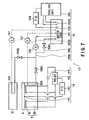
- the wafer temperature control unit 13 will be described by reference to FIG. 7 .
- the wafer temperature control unit 13 is composed of a heater temperature control unit 14 for controlling the temperature of the plane heater 91 and a refrigerant temperature control unit 15 for controlling the temperature of a cooling water supplied to the first cooling jacket 92 and top jacket 12.
- the heater temperature control unit 14 comprises a temperature measuring unit 141 for measuring the temperature of the wafer chuck 2, a first PID adjuster for transmitting a PID control signal on the basis of the deviation of the sense signal from the temperature measuring unit 141 from a preset target value (e.g., 110°C), a relay 143 that operates on the basis of the PID control signal from the first PID adjuster 142, and a heater power supply 144 for controlling the temperature of the plane heater 92 on the basis of the operation of the relay 143.
- a preset target value e.g. 110°C
- a relay 143 that operates on the basis of the PID control signal from the first PID adjuster 142
- a heater power supply 144 for controlling the temperature of the plane heater 92 on the basis of the operation of the relay 143.
- the first PID adjuster 142 transmits a PID control signal to the relay 143 according to the amount of deviation.
- the relay 143 provides PID control of the heater power supply 144, which causes the temperature of the plane heater 92 to coincide with the target value quickly and stably.
- the refrigerant temperature controlling unit 15 comprises a water tank 151 for storing a cooling water for the first cooling jacket 92 and top jacket 12, a cooling unit 152 with a refrigerant pipe 152A immersed in the cooling water of the water tank 151, a temperature sensor 153 for measuring the temperature of the water in the water tank 151, and a second PID adjuster 154 for providing PID control of the cooling unit 152 according to the deviation of the sense signal from the temperature sensor 153 from a preset target value.
- the cooling water is cooled down quickly to the target value according to the deviation of the sense signal from the temperature sensor 153 from the preset target value, and is kept at a stable temperature.
- a supply pipe 155A (indicated by solid lines in FIG. 5 ) and a return pipe 155B (indicated by broken lines in FIG. 5 ) connect the water tank 151 to the inlets and outlets of the refrigerant flow paths 92A and 12A of the first refrigerant jacket 92 and top jacket 12.
- the pipes 155A, 155B enable the cooling water to circulate through the water tank 151, the first cooling jacket 92, and top jacket 12.
- the pipe 155A is separated in the middle in such a manner that one is connected to the inlet of the refrigerant flow path 92A of the first cooling jacket 92 and the other is connected to the inlet of the refrigerant flow path 12A of the top jacket 12.
- a pump 156 is provided on the water tank 151 side of the junction point of the pipe 155A.
- the pump 156 circulates the cooling water.
- the flow rate of the cooling water in the supply path and return path is measured by a flowmeter 157.
- the second PID adjuster 154 transmits a PID control signal to the cooling unit 152 according to the amount of deviation.
- the cooling unit 152 is subjected to PID control, adjusting the flow rate of the refrigerant in the refrigerant pipe 152A, which causes the temperature of the cooling water in the water tank 151 to coincide with the target value quickly and stably.
- the refrigerant temperature control unit 15 provides optimal control of the temperature of the cooling water, enabling the first cooling jacket 92 to cool not only the bottom jacket 9 but also its vicinity.
- the top jacket 12 cools not only the contactor 3 but also its vicinity, which suppresses the rise of the temperature in the temperature control compartment 1A.
- reference symbol 155C indicates a return pipe and 158A, 158B, 158C indicate valves.
- the valves 158A, 158B are closed and the valve 158C is opened, which allows the cooling water to return to the water tank 151.
- the present invention special improvements have been made on the temperature measuring unit 141 of the wafer chuck 2 to enable the wafer chuck 2 to measure the temperature of the wafer W accurately.
- the accurate measurement increases the control accuracy of the wafer temperature control unit 13, which increases the reliability of the reliability test for the wafer W.
- FIGS. 8A and 8B An embodiment of the temperature measuring unit of the wafer chuck according to the present invention will be described by reference to FIGS. 8A and 8B .
- the temperature measuring unit 141 of the present embodiment comprises a rod-like temperature sensor 141A for sensing the temperature of a wafer chuck 2, a cylinder 141C for housing a flange-like piston section 141B formed at the base of the temperature sensor 141A, and a spring 141D which is loaded in the cylinder 141C and constantly urge the temperature sensor 141A upward.
- the temperature measuring units 141 are provided in three places on a base 5 in such a manner that they are set up straight. As shown in FIG. 5 and FIGS. 8A and 8B , the three temperature sensors 141A are inserted in three through holes 9B spaced radially from the center of the bottom jacket 9 to the vicinity of the outer periphery.
- the temperature sensor 141A has a structure where, for example, a thermocouple (or a temperature-measuring resistive element) is inserted in a stainless pipe with a closed tip.
- FIGS. 8A and 8B show all of the temperature measuring unit 141 located in the center of the wafer chuck 2. Regarding the remaining structure of the temperature measuring unit 141, only the tip portion of the temperature sensor 141A is shown.
- each recessed portion 2A has a depth that extends from the back of the wafer chuck 2 to the vicinity of its surface.
- the temperature sensors 141A make elastic contact with the deepest portions of the recessed sections 2A and measure the temperature of the wafer chuck 2 at a position as close to the wafer W as possible.
- the thickness t from the deepest portion of the recessed section 2A to the surface of the wafer chuck is set at, for example, 1 mm.
- the wafer chuck 2 is made of a metallic material excellent in thermal conductivity, such as aluminum, which minimizes the temperature gradient from the wafer surface of the wafer chuck 2 to the deepest portion 2A.
- each of the tips of the three temperature sensors 141A protrudes from the surface of the bottom jacket 9 and goes into the recessed section 2A of the wafer chuck 2.
- each of the tips of the temperature sensors 141A adheres elastically to the deepest portion of the recessed section 2A by means of the spring 141D.
- the temperature of the wafer chuck 2 is measured in the position closest to the wafer W of the wafer chuck 2. Therefore, the temperature closest to the actual temperature of the wafer W is measured.
- the temperature sensors 141A are moved up and down by the spring 141D in the range of, for example, 15 mm.
- a position sensor 141E is provided on the inner surface of the cylinder 141C.
- the position sensor 141E has a square-U-shaped flat structure.
- a shutter 141F provided on the temperature sensor 141A shuts off the light from the position sensor 141E, which enables the position sensor 141E to sense the height of the temperature sensor 141A.
- the position sensor 141E senses the height of the temperature sensor 141A, thereby sensing whether the shell 4 has been placed on the bottom jacket 9.
- a jacket junction unit 16 is provided on the bottom jacket 9 and joins the shell 4 securely to the bottom jacket 9.
- the jacket junction unit 16 includes long bolts 161 and springs 162 surrounding the long bolts 161 and elastically supporting the bottom jacket 9. The long bolts 161 couple the base 5 with the bottom jacket 9 and support them.
- through holes 5A corresponding to the long bolts 161 are made in the base 5 as guide holes at regular intervals along the circumference.
- the bolts 161 penetrate through the through holes 5A and the heads 161B of the long bolts 161 are screwed to the back of the base 5.
- recessed sections in which the long bolts 161 are inserted are formed at regular intervals along the circumference.
- a through hole is made in the center of each recessed section.
- a female thread section 161A is formed at the tip of each long bolt 161. The tip is fitted in the recessed section of the bottom jacket 9.
- the screw 163 inserted from the surface of the bottom jacket 9 into the through hole is screwed to the female thread section 161A. Therefore, the long bolt 161 goes straight down from the bottom jacket 9 and its head stops at the back of the base 5.
- the correction enables the shell 4 to adhere elastically to the entire surface of the bottom jacket 9.
- the shell 4 is level and all the electrode pads 3A of the contactor 3 make in-unison contact with the pogo pins 10 uniformly.
- the expansion and contraction range of the screw 162 is set so that the bottom jacket 9 may move up and down in the range of, for example, 10 mm, when the shell 4 is joined to the bottom jacket 9.
- the spring 141D of the temperature measuring unit 14 may expand and contract in the range of 15 mm when the shell 4 joins to the bottom jacket 9, the expansion and contraction range of the spring 141D has an allowance of 5 mm for the spring 162. Therefore, when the shell 4 joins to the bottom jacket 9, if the bottom jacket 9 goes down 10 mm, the temperature sensor 141A is constantly in elastic contact with the recessed section 2A of the wafer chuck 2.
- a pogo pin block 17 is provided on a support plate 8 ( FIG. 2 ) surrounding the bottom jacket 9.
- Pogo pins 10 are provided on the pogo pin block 17.
- the pogo pin block 17 has a structure where the bottom jacket 9 is divided (in this case, quadrisected) radially at the center of a hole 17A the bottom jacket 9 faces. Each part of the structure is formed into a block element 171. A clearance ⁇ of 1 mm is given between adjacent block elements 171. Each clearance ⁇ absorbs the thermal expansion of each block element 171.
- Such a structure of the pogo pin block 17 decreases changes in the dimensions due to the thermal expansion of the pogo pin block 17. As shown in FIG.
- the pogo pins will move, for example, only from the solid line position to the dot-dash line position, enabling the pogo pins to come into contact with the connection pads 3B of the contactor 3 reliably without coming off the pads 3B. If a pogo pin block 17' is formed into a single block as shown in FIG. 10A , changes in the dimensions of the pogo pin block 17' due to thermal expansion will be large, because the pogo pin block 17' is four times as large as the block element 171. As shown in FIG.
- the pogo pins 10 will move from the solid line position to the dot-dash line position and possibly come off the connection pads 3B of the contactor 3, leading to a decrease in the reliability of the test.
- the pogo pin block 17 shown in FIG. 9A measured 310 mm long, 310 mm wide, and 30 mm thick
- the amount of shift of an outer pogo pin 10 was 300 ⁇ m (see FIG. 9B ).
- the amount of shift of a similar pin was 600 ⁇ m, even when the block 17' was as large as the block 17 of the FIG. 9A .
- the pogo pin block 17 when the pogo pin block 17 is quadrisected and a clearance of ⁇ is given, the amount of shift of the pogo pins 10 is halved, enabling the pogo pins 10 to make into contact with the connection pads 3B of the contactor 3 reliably and stably, which increases the reliability of test. It is desirable that the pogo pin block 17 should be made of synthetic resin, such as glass-fiber-filled polyimide or polyamide-imide resin, formed into a rectangle, and have a thermal coefficient as large as that of the contactor 3.
- synthetic resin such as glass-fiber-filled polyimide or polyamide-imide resin
- guide holes 171A are made.
- the block element 171 On the basis of the guide holes 171A and the guide holes (not shown) made corresponding to the guide holes 171A in the base 5, the block element 171 is located in a specific mounting position.
- fastening holes 171B for fastening members, such as screws, are made in the block elements 171.
- the block element 171 On the basis of the fastening holes 171B and the fastening holes made in the base 5 corresponding to the fastening holes 171B, the block element 171 is secured in a specific mounting position.
- the block elements 171 After guide pins (not shown) have been inserted into the guide holes 171A of the block elements 171 and base 5, the block elements 171 are secured to the base 5 by the fastening members. With this structure, the block elements 171 are fixed securely in the specific mounting positions. It is desirable that the fastening holes in the block elements 171 may have an allowance to absorb changes in the dimensions due to the thermal expansion of the block elements 171.
- the alignment unit aligns the wafer chuck 2, wafer W, and contactor 3 and integrates them into a shell 4.
- the wafer chuck 2 is placed on the main chuck 11 of the alignment unit as shown in FIG. 3B .
- the wafer W is transferred onto the wafer chuck 2.
- the three pins 11A of the main chuck 11 go up, penetrate through the through holes 21D of the wafer chuck 2, protrude from the surface of the wafer chuck 2 while expanding the silicone rubber film 25, and wait to receive the wafer W.
- the contactor 3 is located in a specific position above the main chuck 11. Then, the electrode pads P of the wafer W and the electrode pads 3A of the contactor 3 are read by an imaging element, such as a CCD camera (not shown), finding the coordinates of the positions of representative ones of the electrode pads P of the wafer W. The coordinates of the positions of the electrode pads 3A of the contactor 3 corresponding to the electrode pads P are also found.
- an imaging element such as a CCD camera (not shown)
- the main chuck 11 moves in the directions of X, Y, ⁇ and aligns the electrode pads P with the electrode pads 3A. After the alignment, the main chuck 2 goes up, causing all the electrode pads P to make in-unison contact with the electrode pads 3A corresponding to the pads P.
- the wafer chuck 2 is ready for nitrogen gas replacement and vacuumization through the gas supply and exhaust pipes 22, 23.
- the air between the wafer chuck 2 and contactor 3 is replaced with nitrogen by supplying nitrogen gas through the gas supply pipe 22.
- the nitrogen gas supply source is disconnected from the gas supply pipe 22.
- the valve mechanisms 22A, 23A operate to close the gas flow path 21A.
- the nitrogen gas between the wafer chuck 2 and contactor 3 is exhausted via the gas exhaust pipe 23, the gas flow path 21A, and the ringed grooves 21B, 21C in the surface of the wafer chuck 2.
- the electrode pads P of the wafer W make in-unison contact with the electrode pads of the contactor 3.
- the shell 4 enables all the chips to be tested in unison in the wafer state.
- the anisotropic conductive sheet 31 is capable of absorbing the variations.
- the space between the wafer chuck 2 and contactor 3 is shut off from the outside world by the seal ring 21 provided around the wafer chuck 2 and the through holes 21D for three pins are shut off from the outside world by the silicone rubber film 25. This enables the depressurized state to be maintained reliably when the space between the wafer chuck 2 and contactor 3 has been depressurized.
- the transfer mechanism (not shown) transfers the shell 4 from the alignment unit to the wafer storage chamber 1 as shown in FIG. 1 .
- the clamp mechanism clamps the shell 4.
- the four cylinder mechanisms 6 are actuated, causing the pressure plate 7 to press the shell 4 down to the bottom jacket 9. Even if the shell 4 inclines slightly with respect to the bottom jacket 9 when the shell 4 has reached the bottom jacket 9 as a result of the descent of the pressure plate 7, the inclination will be absorbed by the springs 162 of the jacket junction unit 16, allowing the shell 4 to adhere elastically to the bottom jacket 9.
- the temperature sensors 141A of the temperature measuring unit 141 protrude from the surface of the bottom jacket 9 gradually, and fit into the recessed sections 2A of the wafer chuck 2.
- the temperature sensors 141A touch the deepest portions of the recessed sections 2A.
- the springs 141D cause the tips of the temperature sensors 141A to elastically contact the deepest portions of the recessed sections 2A. This brings the sensors into a state where they can measure the temperature of the wafer chuck 2 in a position only 1 mm away from the wafer W.
- the sensing of the positions of the temperature sensors 141A by the position sensors 141E makes it possible to reliably sense whether the shell 4 exists on the bottom jacket 9.
- the wafer temperature control device 13 heats the wafer W to the test temperature (110°C) and keeps it at that temperature.
- the heater temperature control unit 14 turns on the heater power supply 144 to cause the plane heater 91 to heat the wafer chuck 2 from below.
- the temperature sensors 141A of the temperature measuring unit 141 measure the temperature of the wafer chuck 2 and transmit the sense signals to the PID adjuster 142.
- the PID adjuster 142 transmits to the relay 143 a control signal corresponding to the deviation of the measured temperature from the target value (test temperature).
- the relay 143 subjects the heater power supply 144 to PID control.
- the heater power supply 144 applies the power corresponding to the deviation to the plane heater 91.
- the plane heater 91 raises the temperature of the wafer chuck 2 to the test temperature in a short time.
- the valves 158A, 158B are opened, the pump 156 is driven, and the cooling water in the water tank 151 is supplied through the supply pipe 155A to the first cooling jacket 92 of the bottom jacket 9 and top jacket 12.
- the cooling water passes through the refrigerant flow paths 92A, 12A and the return pipe 155B and returns to the water tank 151, thereby cooling the bottom jacket 9 and top jacket 12.
- the PID adjuster 142 When the temperature of the wafer chuck 2 has reached the test temperature, the PID adjuster 142 operates on the basis of the sense signal from the temperature sensors 141A, subjecting the heater power supply 144 to PID control.
- the PID control enables the power supplied to the heater power supply 144 to be kept at an almost constant level, maintaining the wafer chuck 2 at the test temperature.
- the cooling water absorbs the heat from the plane heater 91 and rises in temperature.
- the heat resistance sheet 93 intervenes between the plane heater 91 and first cooling jacket 92, most of the heat flow from the plane heater 91 to the first cooling jacket 92 is cut off by the heat resistance sheet 93, preventing the temperature of the cooling water from rising excessively. As a result, the cooling water is prevented from boiling in the refrigerant flow path 92A, enabling the bottom jacket 9 to be cooled efficiently.
- the temperature of the cooling water returning from the bottom jacket 9 and top jacket 12 to the water tank 151 has reached about 70 to 80°C.
- the cooling water in the water tank 151 is cooled by the cooling unit 152 to a temperature (e.g., 40°C) at which the cooling efficiency is always good.
- the temperature of the cooling water is constantly sensed by the temperature sensor 153, which transmits the sense signal to the PID adjuster 154.
- the cooling unit 152 is subjected to PID control, constantly adjusting the flow rate of the refrigerant, which constantly keeps the cooling water in the water tank 151 at a constant temperature.
- the first cooling jacket 92 suppresses the rise of the temperature around the bottom jacket 9, but also the top jacket 12 suppresses the temperature rise of the contactor 3 and the rise of the temperature around the contactor 3.
- the temperature rise in the temperature control compartment 1A is suppressed, which suppresses the heat dissipation toward the outside of the wafer storage chamber 1.
- the pogo pin block 17 expands thermally. Changes in the dimensions due to the thermal expansion of the pogo pin block 17 are remarkably small, because the pogo pin block 17 has been divided into four block elements 171, with a 1-mm clearance between the block elements 171. Accordingly, the pogo pins 10 provided on the pogo pin block 17 come into contact with the connection pads 3B of the contactor 3 stably and reliably.
- a test signal S1 is transmitted via the connector, pogo pins 10, and contactor 3 to the wafer W as shown in FIG. 2 .
- a sense result signal S2 from the wafer W is transmitted to the tester in the opposite route. In this way, all the chips are tested in the wafer state.
- the wafer chuck 2 that holds the wafer W making in-unison contact with the contactor 3 is placed on the bottom jacket 9.
- the bottom jacket 9 raises the temperature of the wafer W to a specific test temperature (110°C).
- Three recessed sections 2A are made in the back of the wafer chuck 2 in such a manner that their depth reaches close to the surface of the chuck 2.
- Through holes 9B corresponding to the recessed sections 2A are made in the bottom jacket 9.
- the temperature sensors 141A capable of being inserted into the through holes 9B as far as the recessed sections 2A are provided on the base 5 below the bottom jacket 9.
- the temperature sensors 141A are supported by the springs 141D. During a test, the tips of the temperature sensors 141A are caused to make elastic contact with the recessed sections 2A. This enables the temperature sensors 141A to be located near the wafer W during the test in the wafer storage chamber 1, making it possible to measure the temperature of the wafer chuck 2 and consequently the temperature of the wafer W accurately, which increases the accuracy of the test.
- the position sensor 141E is provided which senses whether the wafer chuck 2 (the shell 4 in the embodiment) exists on the bottom jacket 9.
- the position sensor 141E makes it possible to reliably sense whether the shell 4 has been mounted on the bottom jacket 9 and measure the temperature of the wafer W without error.
- a temperature control mechanism has been installed as the bottom jacket 9 on the base 5 in the wafer storage chamber 1, the temperature control mechanism may be provided as a top jacket on the top surface of the wafer storage chamber 1.
- the wafer storage chamber 1 has been arranged horizontally, it may be arranged vertically. In this case, depending on the relative positional relationship between the temperature control mechanism in the wafer storage chamber 1 and the wafer hold table, the temperature sensors of the temperature measuring unit are able to make elastic contact with the wafer hold table from above or from one side.
- the jacket junction unit 16 joining the chuck 2 to the bottom jacket 9 includes long bolts 161 extending in the direction in which the bottom jacket 9 moves up and down and springs 162 arranged around the long bolts 161 and elastically supporting the bottom jacket 9.
- the jacket junction unit 16 presses the entire wafer chuck 2 against the entire bottom jacket 9 uniformly and elastically when the chuck 2 is joined to the jacket 9. As a result, the heat transfer rate between the chuck 2 and the bottom jacket 9 is increased, making it possible not only to heat the wafer W swiftly during the test but also keep the wafer at the test temperature accurately, which increases the reliability of the test.
- the springs 162 have been used as elastic members in the jacket junction unit 16, parts other than springs may be used as the elastic members.
- the elastic members may be provided in a place different from the long bolts 161.
- the temperature control mechanism may be provided as a top jacket on the ceiling of the wafer storage chamber 1.
- the heater control unit 14 and refrigerant temperature control unit 15 include the PID adjusters 142, 154 respectively, the cooling water in the wafer chuck 2 and water tank 151 is set at the target temperature quickly on the basis of the sense signals from the temperature sensors 141, 153. This enables the temperature of the cooling water to be kept at the target temperature stably.
- the temperature sensors 141A penetrate through the bottom jacket 9 and make elastic contact with the recessed sections 2A of the wafer chuck 2, which enables the temperature of the wafer W to be measured accurately.
- the wafer W is cooled stably at low cost.
- the wafer chuck 2 comprises the body 21 holding the wafer W, the openings in the surface of the body 21, the gas flow path 21A formed in the body 21 and connected to the openings, the valve mechanisms 22A, 23A provided to the inlet and outlet of the gas flow path 21A, and the seal ring 24 provided on all of the periphery of the surface of the body 21.
- the through holes 21D are made in the body 21. The through holes 21D enable the three pins 11A of the main chuck 11 to move up and down when the wafer W is placed on or removed from the surface of the body 21.
- each of the through holes 21D is provided with the silicone rubber film 25 that expands and contracts as the three pins 11A move up and down, the three pins 11A of the main chuck 11 go into and out of the through holes 21D when the wafer W is placed on and removed from the wafer chuck 2. In this way, the three pins 11A enables the wafer W to be placed on and removed from the chuck smoothly.
- the space between the body 21 of the main chuck 2 and the contactor is vacuumized via the gas supply pipe 22 and exhaust pipe 23.
- the vacuum state is maintained because the space between the body 21 of the main chuck 2 and the contactor 3 is sealed by the seal ring 24 and silicone rubber film 25 and the gas supply pipe 22 and gas exhaust pipe 23 are closed by the valve mechanisms 22A, 23A.
- the transfer mechanism transfers the shell 4 easily to the wafer storage chamber 1.
- the silicone rubber film 25 is formed into a cylinder whose tip is sealed and whose lower end is open, according to the shape of the three pins 11A, it may be fit into the through hole 21D.
- the silicone rubber film 25 expands and contracts readily as the three pins 11A move up and down, which allows the three pins 11A to go up and down smoothly.
- the wafer holding table can be used not only suitably as a wafer chuck 2 for test that causes a wafer W to make in-unison contact with the contactor but also widely as a carrier to transfer wafers one by one.
- the wafer holding table of the invention and its related component parts are not restricted to those in the embodiment. Each component part may be changed as the occasion demands.
- the pogo pin block 17 that supports the pogo pins 10 for connecting the contactor 3 to the connector is quadrisected, with a clearance ⁇ between the divided parts, even when the pogo pin block 17 expands thermally as a result of the rise of the temperature in the temperature control compartment 1A, the thermal expansion of the pogo pin block 17 is small and the pogo pins 10 on the pogo pin block 17 contact the connection pads 3B of the contactor 3 reliably, assuring a stable electrical conduction between the pogo pins 10 and connection pads 3B, which increases the reliability of test.
- the pogo pin block 17 has been quadrisected, it is not limited to quadrisection.
Landscapes
- Testing Or Measuring Of Semiconductors Or The Like (AREA)
- Container, Conveyance, Adherence, Positioning, Of Wafer (AREA)
- Testing Of Individual Semiconductor Devices (AREA)
Claims (9)
- Appareil de maintien de plaquette de semi-conducteur comprenant :un contacteur (3) incluant une pluralité de moyens conducteurs (31B) qui établissent un contact électrique, à l'unisson, avec des électrodes spécifiques (P) d'éléments à semi-conducteur formés sur une plaquette de semi-conducteur (W) et des bornes externes électriquement reliées aux moyens conducteurs (31B) ;une table de maintien de plaquette de semi-conducteur (2) pour maintenir la plaquette de semi-conducteur (W) en contact avec ledit contacteur (3) dans lequel la table de maintien de plaquette (2), la plaquette (W) et le contacteur (3) sont intégrés dans une enveloppe formant entité unique (4) ;un mécanisme de mesure de température (141) pour mesurer la température de la table de maintien de plaquette de semi-conducteur (2) ; etun mécanisme de commande de température (9) pour commander la température de la plaquette de semi-conducteur (W) placée sur la table de maintien de plaquette de semi-conducteur (2),dans lequel ledit mécanisme de mesure de température (141) inclut au moins un capteur de température (141A), un premier élément de support élastique (141D) qui supporte le capteur de température, permet au capteur de température (141A) de passer à travers un trou traversant (9B) dans ledit mécanisme de commande de température, et ajuste le capteur de température dans une section en retrait (2A) de ladite table de maintien de plaquette de semi-conducteur (2),une plaque de support (8) qui a un trou (8A), le mécanisme de commande de température (13) étant disposé dans ledit trou (8A), des bornes de jonction (10) étant agencées autour dudit trou (8A), les bornes de jonction (10) correspondant aux bornes externes du contacteur, et les bornes de jonction (10) étant reliées à un appareil de mesure qui mesure la caractéristique électrique de l'élément à semi-conducteur formé sur la plaquette de semi-conducteur, etun mécanisme (6) qui déplace l'enveloppe vers le haut et vers le bas dans lequel, lorsque le mécanisme (6) déplace l'enveloppe vers le bas, l'arrière de la table de maintien de plaquette (2) entre en contact avec la surface du mécanisme de commande de température (9) et est monté sur la surface de sorte que les bornes externes de l'enveloppe entrent en contact avec les bornes de jonction (10) sur la plaque de support ;et dans lequel ledit mécanisme de commande de température (9) est supporté par un mécanisme de support qui inclutune base (5) dans laquelle des trous traversants (5A) sont faits,des tiges (161) qui pénètrent à travers les trous traversants (5A) dans la base (5) et qui sont fixées audit mécanisme de commande de température (9) et qui guident ladite base (5) de telle sorte que la base puisse se déplacer de manière relative par rapport audit mécanisme de commande de température, etdes seconds éléments de support élastiques (162) pour supporter ledit mécanisme de commande de température (9) de manière élastique d'une façon qui laisse un espace entre le mécanisme de commande de température (9) et ladite base (5) ; etun mécanisme qui supporte de manière élastique le mécanisme de commande de température (9) dans le trou (8A) formé sur la plaque de support (8).
- Appareil de maintien de plaquette de semi-conducteur selon la revendication 1, caractérisé en ce que lesdits seconds éléments de support élastiques sont des ressorts hélicoïdaux (162) enroulés autour desdites tiges (161).
- Appareil de maintien de plaquette de semi-conducteur selon la revendication 1, caractérisé en ce que ledit au moins un capteur de température (141A) est supporté sur la table de maintien de plaquette de semi-conducteur (2) par l'intermédiaire du premier élément de support élastique (141D).
- Appareil de maintien de plaquette de semi-conducteur selon la revendication 1, caractérisé en ce que ledit mécanisme de mesure de température (141) est muni d'un capteur de position (141E) pour détecter la position d'au moins un capteur de température (141A).
- Appareil de maintien de plaquette de semi-conducteur selon la revendication 1, caractérisé en ce que ledit mécanisme de commande de température (9) inclut
un élément chauffant (91) disposé à l'intérieur du mécanisme de commande de température (9) et près de la surface du mécanisme,
un passage de refroidissement qui est prévu dans le mécanisme de commande de température (9) avec un dégagement par rapport à l'élément chauffant et à travers lequel un réfrigérant (92A) passe, et
une feuille résistant à la chaleur (93) disposée entre le passage de refroidissement et l'élément chauffant,
dans lequel le mécanisme de commande de température (9) établit un contact avec ladite table de maintien de plaquette de semi-conducteur (2) pour supporter la table, et commande la quantité de chauffage par l'élément chauffant (91) et la quantité de refroidissement par le réfrigérant (92A) sur la base de la sortie de signal de détection en provenance dudit mécanisme de mesure de température (141). - Appareil de maintien de plaquette de semi-conducteur selon la revendication 5, caractérisé en ce que ledit mécanisme de commande de température (9) pour commander la quantité de chauffage par l'élément chauffant (91) et la quantité de refroidissement par le réfrigérant (92A) est muni d'un dispositif de régale du type PID (142).
- Appareil de maintien de plaquette de semi-conducteur selon la revendication 5, caractérisé en ce que ledit réfrigérant est de l'eau.
- Appareil de maintien de plaquette de semi-conducteur selon la revendication 1, caractérisé en ce que ladite table de maintien de plaquette de semi-conducteur (2) comprend un corps de mandrin (21) sur lequel une plaquette de semi-conducteur (W) doit être placée, le corps de mandrin (21) incluant :des trous (21D) qui permettent à des ergots (11A) de recevoir et de donner à la plaquette de semi-conducteur un mouvement ascendant et descendant, etun film d'étanchéité (25) qui recouvre les trous et se dilate et se contracte lorsque les ergots montent et descendent.
- Appareil de maintien de plaquette de semi-conducteur selon la revendication 8, caractérisé en ce que ledit film d'étanchéité est fait de caoutchouc de silicone et est sous la forme d'un cylindre dont le bout est scellé et dont l'extrémité inférieure est ouverte.
Applications Claiming Priority (15)
| Application Number | Priority Date | Filing Date | Title |
|---|---|---|---|
| JP318919/97 | 1997-11-05 | ||
| JP31891997 | 1997-11-05 | ||
| JP31892197A JP3368461B2 (ja) | 1997-11-05 | 1997-11-05 | シェル |
| JP31892197 | 1997-11-05 | ||
| JP318921/97 | 1997-11-05 | ||
| JP31892097 | 1997-11-05 | ||
| JP318918/97 | 1997-11-05 | ||
| JP31891897 | 1997-11-05 | ||
| JP31891897A JP3294174B2 (ja) | 1997-11-05 | 1997-11-05 | ウエハ保持体の温度測定装置及びウエハ収納室 |
| JP31892297A JP3294175B2 (ja) | 1997-11-05 | 1997-11-05 | 信頼性試験用ウエハ収納室 |
| JP31892297 | 1997-11-05 | ||
| JP318920/97 | 1997-11-05 | ||
| JP31891997A JP3467548B2 (ja) | 1997-11-05 | 1997-11-05 | 温度制御体の接合装置及びウエハ収納室 |
| JP31892097A JP3400692B2 (ja) | 1997-11-05 | 1997-11-05 | ウエハ温度制御装置及びウエハ収納室 |
| JP318922/97 | 1997-11-05 |
Publications (3)
| Publication Number | Publication Date |
|---|---|
| EP0915499A2 EP0915499A2 (fr) | 1999-05-12 |
| EP0915499A3 EP0915499A3 (fr) | 2004-06-02 |
| EP0915499B1 true EP0915499B1 (fr) | 2011-03-23 |
Family
ID=27531096
Family Applications (1)
| Application Number | Title | Priority Date | Filing Date |
|---|---|---|---|
| EP98120148A Expired - Lifetime EP0915499B1 (fr) | 1997-11-05 | 1998-10-27 | Support pour plaquette semiconductrice |
Country Status (5)
| Country | Link |
|---|---|
| US (1) | US6084215A (fr) |
| EP (1) | EP0915499B1 (fr) |
| KR (1) | KR100342016B1 (fr) |
| DE (1) | DE69842191D1 (fr) |
| TW (1) | TW392274B (fr) |
Families Citing this family (96)
| Publication number | Priority date | Publication date | Assignee | Title |
|---|---|---|---|---|
| WO1999048139A2 (fr) * | 1998-03-18 | 1999-09-23 | Applied Materials, Inc. | Appareil de reduction de perte de chaleur |
| JP3282800B2 (ja) * | 1998-05-20 | 2002-05-20 | 東京エレクトロン株式会社 | アライナー |
| US6583638B2 (en) * | 1999-01-26 | 2003-06-24 | Trio-Tech International | Temperature-controlled semiconductor wafer chuck system |
| JP2001007165A (ja) * | 1999-06-21 | 2001-01-12 | Mitsubishi Electric Corp | プローブカード装置 |
| US6214121B1 (en) | 1999-07-07 | 2001-04-10 | Applied Materials, Inc. | Pedestal with a thermally controlled platen |
| CN100492040C (zh) * | 1999-07-14 | 2009-05-27 | Aehr测试体系 | 晶片级老化和测试盒 |
| US6340895B1 (en) * | 1999-07-14 | 2002-01-22 | Aehr Test Systems, Inc. | Wafer-level burn-in and test cartridge |
| US6562636B1 (en) * | 1999-07-14 | 2003-05-13 | Aehr Test Systems | Wafer level burn-in and electrical test system and method |
| US6580283B1 (en) * | 1999-07-14 | 2003-06-17 | Aehr Test Systems | Wafer level burn-in and test methods |
| EP1199908A4 (fr) * | 1999-10-22 | 2003-01-22 | Ibiden Co Ltd | Plaque chauffante en ceramique |
| US6481886B1 (en) * | 2000-02-24 | 2002-11-19 | Applied Materials Inc. | Apparatus for measuring pedestal and substrate temperature in a semiconductor wafer processing system |
| US6650135B1 (en) * | 2000-06-29 | 2003-11-18 | Motorola, Inc. | Measurement chuck having piezoelectric elements and method |
| US6353210B1 (en) * | 2000-04-11 | 2002-03-05 | Applied Materials Inc. | Correction of wafer temperature drift in a plasma reactor based upon continuous wafer temperature measurements using and in-situ wafer temperature optical probe |
| US6717115B1 (en) * | 2000-04-25 | 2004-04-06 | Teradyne, Inc. | Semiconductor handler for rapid testing |
| EP1225790A1 (fr) * | 2000-05-02 | 2002-07-24 | Ibiden Co., Ltd. | Dispositif de chauffage en ceramique |
| JP2002043381A (ja) * | 2000-07-19 | 2002-02-08 | Tokyo Electron Ltd | ウエハ温度制御装置 |
| US6541989B1 (en) * | 2000-09-29 | 2003-04-01 | Motorola, Inc. | Testing device for semiconductor components and a method of using the device |
| US6441606B1 (en) | 2000-10-17 | 2002-08-27 | Micron Technology, Inc. | Dual zone wafer test apparatus |
| US7080940B2 (en) * | 2001-04-20 | 2006-07-25 | Luxtron Corporation | In situ optical surface temperature measuring techniques and devices |
| US6572265B1 (en) * | 2001-04-20 | 2003-06-03 | Luxtron Corporation | In situ optical surface temperature measuring techniques and devices |
| JP4549022B2 (ja) * | 2001-04-30 | 2010-09-22 | ラム リサーチ コーポレイション | ワーク支持体の表面を横切る空間温度分布を制御する方法および装置 |
| US20050211385A1 (en) * | 2001-04-30 | 2005-09-29 | Lam Research Corporation, A Delaware Corporation | Method and apparatus for controlling spatial temperature distribution |
| US6847014B1 (en) * | 2001-04-30 | 2005-01-25 | Lam Research Corporation | Method and apparatus for controlling the spatial temperature distribution across the surface of a workpiece support |
| US6668570B2 (en) * | 2001-05-31 | 2003-12-30 | Kryotech, Inc. | Apparatus and method for controlling the temperature of an electronic device under test |
| US20030016727A1 (en) * | 2001-06-29 | 2003-01-23 | Tokyo Electron Limited | Method of and apparatus for measuring and controlling substrate holder temperature using ultrasonic tomography |
| US7334826B2 (en) * | 2001-07-13 | 2008-02-26 | Semitool, Inc. | End-effectors for handling microelectronic wafers |
| US7281741B2 (en) * | 2001-07-13 | 2007-10-16 | Semitool, Inc. | End-effectors for handling microelectronic workpieces |
| JP3639546B2 (ja) * | 2001-07-25 | 2005-04-20 | 株式会社日立国際電気 | 基板処理装置及び半導体装置の製造方法 |
| JP4173306B2 (ja) * | 2001-11-30 | 2008-10-29 | 東京エレクトロン株式会社 | 信頼性評価試験装置、信頼性評価試験システム及び信頼性評価試験方法 |
| US6847218B1 (en) * | 2002-05-13 | 2005-01-25 | Cypress Semiconductor Corporation | Probe card with an adapter layer for testing integrated circuits |
| US20070014656A1 (en) * | 2002-07-11 | 2007-01-18 | Harris Randy A | End-effectors and associated control and guidance systems and methods |
| US20060043750A1 (en) * | 2004-07-09 | 2006-03-02 | Paul Wirth | End-effectors for handling microfeature workpieces |
| US7100389B1 (en) | 2002-07-16 | 2006-09-05 | Delta Design, Inc. | Apparatus and method having mechanical isolation arrangement for controlling the temperature of an electronic device under test |
| US6976822B2 (en) * | 2002-07-16 | 2005-12-20 | Semitool, Inc. | End-effectors and transfer devices for handling microelectronic workpieces |
| US6759865B1 (en) | 2002-07-30 | 2004-07-06 | Cypress Semiconductor Corporation | Array of dice for testing integrated circuits |
| US6695886B1 (en) * | 2002-08-22 | 2004-02-24 | Axcelis Technologies, Inc. | Optical path improvement, focus length change compensation, and stray light reduction for temperature measurement system of RTP tool |
| US6838646B2 (en) * | 2002-08-22 | 2005-01-04 | Sumitomo Osaka Cement Co., Ltd. | Susceptor device |
| JP3671951B2 (ja) * | 2002-10-08 | 2005-07-13 | 住友電気工業株式会社 | 測温装置及びそれを用いたセラミックスヒータ |
| US6907742B2 (en) * | 2002-12-19 | 2005-06-21 | Taiwan Semiconductor Manufacturing Co., Ltd | Apparatus and method for controlling wafer temperature |
| US6770852B1 (en) | 2003-02-27 | 2004-08-03 | Lam Research Corporation | Critical dimension variation compensation across a wafer by means of local wafer temperature control |
| US6975028B1 (en) | 2003-03-19 | 2005-12-13 | Delta Design, Inc. | Thermal apparatus for engaging electronic device |
| US7230204B2 (en) * | 2003-03-28 | 2007-06-12 | Tokyo Electron Limited | Method and system for temperature control of a substrate |
| DE602004003365T2 (de) * | 2003-05-07 | 2007-09-13 | Axcelis Technologies, Inc., Beverly | Halterungssystem einsetzbar über einen breiten temperaturbereich |
| KR100536610B1 (ko) * | 2003-08-29 | 2005-12-14 | 삼성전자주식회사 | 프로브 스테이션 교정 도구 |
| US7355428B2 (en) * | 2004-01-14 | 2008-04-08 | Delta Design, Inc. | Active thermal control system with miniature liquid-cooled temperature control device for electronic device testing |
| US20050189342A1 (en) * | 2004-02-23 | 2005-09-01 | Samer Kabbani | Miniature fluid-cooled heat sink with integral heater |
| US7394271B2 (en) * | 2004-02-27 | 2008-07-01 | Wells-Cti, Llc | Temperature sensing and prediction in IC sockets |
| CN101421822B (zh) * | 2004-03-17 | 2010-08-18 | 科福罗科学解决方案有限公司 | 非接触式加热平台 |
| US7332921B2 (en) * | 2004-03-26 | 2008-02-19 | Cypress Semiconductor Corporation | Probe card and method for constructing same |
| US20070020080A1 (en) * | 2004-07-09 | 2007-01-25 | Paul Wirth | Transfer devices and methods for handling microfeature workpieces within an environment of a processing machine |
| DE102004055449B4 (de) * | 2004-11-17 | 2008-10-23 | Steag Hamatech Ag | Verfahren und Vorrichtung zum thermischen Behandeln von Substraten |
| US7731798B2 (en) * | 2004-12-01 | 2010-06-08 | Ultratech, Inc. | Heated chuck for laser thermal processing |
| US7330038B2 (en) * | 2004-12-14 | 2008-02-12 | Silicon Light Machines Corporation | Interleaved MEMS-based probes for testing integrated circuits |
| JP4436371B2 (ja) * | 2004-12-27 | 2010-03-24 | 株式会社日立国際電気 | 温度調整方法、熱処理装置、半導体装置の製造方法 |
| US8038796B2 (en) * | 2004-12-30 | 2011-10-18 | Lam Research Corporation | Apparatus for spatial and temporal control of temperature on a substrate |
| JP4356661B2 (ja) * | 2005-07-25 | 2009-11-04 | 住友電気工業株式会社 | ウェハ保持体およびそれを搭載したウェハプローバ |
| JP2007042911A (ja) * | 2005-08-04 | 2007-02-15 | Sumitomo Electric Ind Ltd | ウェハ保持体およびそれを搭載したウェハプローバ |
| JP4667158B2 (ja) * | 2005-08-09 | 2011-04-06 | パナソニック株式会社 | ウェーハレベルバーンイン方法 |
| JP3972944B2 (ja) * | 2005-09-12 | 2007-09-05 | 住友電気工業株式会社 | セラミックスヒータ及びそれを備えた半導体製造装置 |
| US7755742B2 (en) * | 2005-10-11 | 2010-07-13 | Asml Netherlands B.V. | Lithographic apparatus with mounted sensor |
| CN100492021C (zh) * | 2005-10-14 | 2009-05-27 | 旺矽科技股份有限公司 | 用于探针装置的定位件 |
| CN100361288C (zh) * | 2005-12-07 | 2008-01-09 | 北京北方微电子基地设备工艺研究中心有限责任公司 | 控制静电卡盘温度系统 |
| US7906982B1 (en) | 2006-02-28 | 2011-03-15 | Cypress Semiconductor Corporation | Interface apparatus and methods of testing integrated circuits using the same |
| US8573836B2 (en) * | 2006-10-26 | 2013-11-05 | Tokyo Electron Limited | Apparatus and method for evaluating a substrate mounting device |
| US20080160462A1 (en) * | 2007-01-03 | 2008-07-03 | Sokudo Co., Ltd. | Method and system for bake plate heat transfer control in track lithography tools |
| JP4564973B2 (ja) | 2007-01-26 | 2010-10-20 | 株式会社日立ハイテクノロジーズ | プラズマ処理装置 |
| WO2009004968A1 (fr) * | 2007-06-29 | 2009-01-08 | Advantest Corporation | Appareil de test |
| US7651269B2 (en) * | 2007-07-19 | 2010-01-26 | Lam Research Corporation | Temperature probes having a thermally isolated tip |
| US7500781B1 (en) * | 2007-10-25 | 2009-03-10 | Sokudo Co., Ltd. | Method and apparatus for detecting substrate temperature in a track lithography tool |
| US7800382B2 (en) | 2007-12-19 | 2010-09-21 | AEHR Test Ststems | System for testing an integrated circuit of a device and its method of use |
| US8030957B2 (en) | 2009-03-25 | 2011-10-04 | Aehr Test Systems | System for testing an integrated circuit of a device and its method of use |
| KR100990198B1 (ko) * | 2009-08-07 | 2010-10-29 | 가부시키가이샤 어드밴티스트 | 웨이퍼 트레이 및 시험 장치 |
| US9176186B2 (en) * | 2009-08-25 | 2015-11-03 | Translarity, Inc. | Maintaining a wafer/wafer translator pair in an attached state free of a gasket disposed |
| NL2008751A (en) | 2011-06-06 | 2012-12-10 | Asml Netherlands Bv | Temperature sensing probe, burl plate, lithographic apparatus and method. |
| US9759772B2 (en) | 2011-10-28 | 2017-09-12 | Teradyne, Inc. | Programmable test instrument |
| US10776233B2 (en) | 2011-10-28 | 2020-09-15 | Teradyne, Inc. | Programmable test instrument |
| CN103208440B (zh) * | 2012-01-17 | 2016-01-20 | 中国科学院微电子研究所 | 腔室加热装置 |
| JP6246685B2 (ja) * | 2014-09-12 | 2017-12-13 | 株式会社東芝 | 静電チャック機構、基板処理方法及び半導体基板処理装置 |
| KR102842851B1 (ko) | 2016-01-08 | 2025-08-05 | 에어 테스트 시스템즈 | 일렉트로닉스 테스터 내의 디바이스들의 열 제어를 위한 방법 및 시스템 |
| KR102219361B1 (ko) * | 2016-03-28 | 2021-02-23 | 가부시키가이샤 코쿠사이 엘렉트릭 | 기판 처리 장치, 온도 측정 유닛 및 반도체 장치의 제조 방법 |
| US11061069B2 (en) | 2016-06-02 | 2021-07-13 | Kes Systems, Inc. | Burn-in test apparatus for semiconductor devices |
| US10393592B2 (en) * | 2016-12-21 | 2019-08-27 | Intel Corporation | Systems and methods for measuring surface temperature |
| JP6839556B2 (ja) * | 2017-02-08 | 2021-03-10 | リンナイ株式会社 | 熱交換器 |
| US10649022B2 (en) | 2017-03-03 | 2020-05-12 | Aehr Test Systems | Electronics tester |
| KR102222455B1 (ko) * | 2018-01-15 | 2021-03-04 | 세메스 주식회사 | 기판 처리 장치 |
| JP7154160B2 (ja) * | 2019-03-18 | 2022-10-17 | 東京エレクトロン株式会社 | 温度測定機構、温度測定方法、およびステージ装置 |
| EP4226165A4 (fr) | 2020-10-07 | 2024-10-30 | AEHR Test Systems | Appareil d'essai électronique |
| CN112735966A (zh) * | 2020-12-25 | 2021-04-30 | 广州粤芯半导体技术有限公司 | 腔室温度监测方法 |
| JP7511498B2 (ja) | 2021-02-01 | 2024-07-05 | 三菱電機株式会社 | 半導体試験装置および半導体試験方法 |
| CN112946010B (zh) * | 2021-02-07 | 2021-12-28 | 宏茂科技(珠海)有限公司 | 一种用于半导体纳米材料热性能测试装置 |
| JP2022125685A (ja) * | 2021-02-17 | 2022-08-29 | 株式会社Kelk | 半導体ウエハの温度制御装置及び半導体ウエハの温度制御方法 |
| EP4318246A4 (fr) | 2021-03-23 | 2025-02-19 | Kioxia Corporation | Système de stockage |
| US12092183B2 (en) * | 2021-08-10 | 2024-09-17 | Kla Corporation | Spring mechanism for self-lock and centering during loading |
| CN121114723A (zh) | 2022-12-30 | 2025-12-12 | 雅赫测试系统公司 | 电子测试器 |
| CN117214676B (zh) * | 2023-11-09 | 2024-01-23 | 成都梓峡信息技术有限公司 | 一种fpga老炼测试系统 |
| KR102873095B1 (ko) * | 2024-07-22 | 2025-10-20 | 주식회사 피앤에스인터내셔날 | 반도체 공정부품 형상 측정장치 |
Family Cites Families (41)
| Publication number | Priority date | Publication date | Assignee | Title |
|---|---|---|---|---|
| US4147571A (en) * | 1977-07-11 | 1979-04-03 | Hewlett-Packard Company | Method for vapor epitaxial deposition of III/V materials utilizing organometallic compounds and a halogen or halide in a hot wall system |
| GB2069299B (en) * | 1980-01-30 | 1983-06-22 | Riccar Co Ltd | Induction heating apparatus |
| US4551192A (en) * | 1983-06-30 | 1985-11-05 | International Business Machines Corporation | Electrostatic or vacuum pinchuck formed with microcircuit lithography |
| US4609037A (en) * | 1985-10-09 | 1986-09-02 | Tencor Instruments | Apparatus for heating and cooling articles |
| US4788416A (en) * | 1987-03-02 | 1988-11-29 | Spectrum Cvd, Inc. | Direct wafer temperature control |
| US4955590A (en) * | 1988-12-08 | 1990-09-11 | Tokyo Electron Limited | Plate-like member receiving apparatus |
| US5198752A (en) * | 1987-09-02 | 1993-03-30 | Tokyo Electron Limited | Electric probing-test machine having a cooling system |
| US4944860A (en) * | 1988-11-04 | 1990-07-31 | Eaton Corporation | Platen assembly for a vacuum processing system |
| EP0447155B1 (fr) * | 1990-03-12 | 1995-07-26 | Ngk Insulators, Ltd. | Calorifères pour pastilles semi-conductrices pour un appareil produisant des semi-conducteurs, unités de chauffage utilisant de tels calorifères, et production de calorifères |
| GB9010833D0 (en) * | 1990-05-15 | 1990-07-04 | Electrotech Research Limited | Workpiece support |
| US5238499A (en) * | 1990-07-16 | 1993-08-24 | Novellus Systems, Inc. | Gas-based substrate protection during processing |
| JP2892787B2 (ja) * | 1990-07-20 | 1999-05-17 | 東京エレクトロン株式会社 | 電気信号の抽出方法 |
| EP0484179B1 (fr) * | 1990-11-01 | 1996-03-27 | Canon Kabushiki Kaisha | Dispositif de maintien d'un plaquette pour appareil d'exposition |
| US5378971A (en) * | 1990-11-30 | 1995-01-03 | Tokyo Electron Limited | Probe and a method of manufacturing the same |
| JP3014770B2 (ja) * | 1990-12-20 | 2000-02-28 | 富士通株式会社 | 半導体製造装置 |
| JPH04364746A (ja) * | 1991-06-12 | 1992-12-17 | Tokyo Electron Yamanashi Kk | プローブ装置 |
| US5294778A (en) * | 1991-09-11 | 1994-03-15 | Lam Research Corporation | CVD platen heater system utilizing concentric electric heating elements |
| KR100248571B1 (ko) * | 1992-08-31 | 2000-03-15 | 히가시 데쓰로 | 프로우브 장치 |
| JP3049981B2 (ja) * | 1992-12-04 | 2000-06-05 | 株式会社村田製作所 | チップ部品の電極形成システム |
| US5665167A (en) * | 1993-02-16 | 1997-09-09 | Tokyo Electron Kabushiki Kaisha | Plasma treatment apparatus having a workpiece-side electrode grounding circuit |
| US5366002A (en) * | 1993-05-05 | 1994-11-22 | Applied Materials, Inc. | Apparatus and method to ensure heat transfer to and from an entire substrate during semiconductor processing |
| US5656945A (en) * | 1993-05-12 | 1997-08-12 | Tribotech | Apparatus for testing a nonpackaged die |
| US5329097A (en) * | 1993-05-19 | 1994-07-12 | The United States Of America As Represented By The Secretary Of The Navy | Compact substrate heater for use in an oxidizing atmosphere |
| US5511799A (en) * | 1993-06-07 | 1996-04-30 | Applied Materials, Inc. | Sealing device useful in semiconductor processing apparatus for bridging materials having a thermal expansion differential |
| US5591269A (en) * | 1993-06-24 | 1997-01-07 | Tokyo Electron Limited | Vacuum processing apparatus |
| US5570032A (en) * | 1993-08-17 | 1996-10-29 | Micron Technology, Inc. | Wafer scale burn-in apparatus and process |
| JPH07161788A (ja) * | 1993-12-03 | 1995-06-23 | Tokyo Electron Ltd | バーンイン用コンタクタ及びプローブカード |
| KR0140034B1 (ko) * | 1993-12-16 | 1998-07-15 | 모리시다 요이치 | 반도체 웨이퍼 수납기, 반도체 웨이퍼의 검사용 집적회로 단자와 프로브 단자와의 접속방법 및 그 장치, 반도체 집적회로의 검사방법, 프로브카드 및 그 제조방법 |
| JP2828410B2 (ja) * | 1993-12-21 | 1998-11-25 | 松下電器産業株式会社 | プローブカード及び半導体チップの検査方法 |
| JP2925964B2 (ja) * | 1994-04-21 | 1999-07-28 | 松下電器産業株式会社 | 半導体ウェハ収納器及び半導体集積回路の検査方法 |
| US5730801A (en) * | 1994-08-23 | 1998-03-24 | Applied Materials, Inc. | Compartnetalized substrate processing chamber |
| JP2830757B2 (ja) * | 1994-12-01 | 1998-12-02 | 日本電気株式会社 | シリコン・テスタの測定治具 |
| JPH08340030A (ja) * | 1995-04-13 | 1996-12-24 | Tokyo Electron Ltd | バーンイン装置およびバーンイン用ウエハトレイ |
| EP0743530A3 (fr) * | 1995-05-16 | 1997-04-09 | Trio Tech International | Dispositif de test de composants électroniques |
| JPH09145485A (ja) * | 1995-11-28 | 1997-06-06 | Kokusai Electric Co Ltd | 温度検出装置 |
| US5885353A (en) * | 1996-06-21 | 1999-03-23 | Micron Technology, Inc. | Thermal conditioning apparatus |
| US5811762A (en) * | 1996-09-25 | 1998-09-22 | Taiwan Semiconductor Manufacturing Company, Ltd. | Heater assembly with dual temperature control for use in PVD/CVD system |
| US5756157A (en) * | 1996-10-02 | 1998-05-26 | Silicon Valley Group | Method for processing flat panel displays and large wafers |
| EP0837333A3 (fr) * | 1996-10-18 | 1999-06-09 | Tokyo Electron Limited | Dispositif pour aligner une tranche semi-conductrice avec un connecteur de test |
| JPH10256325A (ja) * | 1997-03-07 | 1998-09-25 | Orion Mach Co Ltd | 半導体ウェーハの試験装置用温度調節プレート |
| US5844208A (en) * | 1997-04-04 | 1998-12-01 | Unisys Corporation | Temperature control system for an electronic device in which device temperature is estimated from heater temperature and heat sink temperature |
-
1998
- 1998-10-27 DE DE69842191T patent/DE69842191D1/de not_active Expired - Lifetime
- 1998-10-27 EP EP98120148A patent/EP0915499B1/fr not_active Expired - Lifetime
- 1998-10-27 US US09/179,192 patent/US6084215A/en not_active Expired - Lifetime
- 1998-11-04 KR KR1019980047147A patent/KR100342016B1/ko not_active Expired - Fee Related
- 1998-11-04 TW TW087118374A patent/TW392274B/zh not_active IP Right Cessation
Also Published As
| Publication number | Publication date |
|---|---|
| EP0915499A3 (fr) | 2004-06-02 |
| KR19990045000A (ko) | 1999-06-25 |
| KR100342016B1 (ko) | 2002-09-18 |
| TW392274B (en) | 2000-06-01 |
| EP0915499A2 (fr) | 1999-05-12 |
| DE69842191D1 (de) | 2011-05-05 |
| US6084215A (en) | 2000-07-04 |
Similar Documents
| Publication | Publication Date | Title |
|---|---|---|
| US6084215A (en) | Semiconductor wafer holder with spring-mounted temperature measurement apparatus disposed therein | |
| US20020014894A1 (en) | Temperature control apparatus | |
| CN1920585B (zh) | 基板检查装置 | |
| US11313897B2 (en) | Testing wafer and testing method | |
| US6130543A (en) | Inspection method and apparatus for semiconductor integrated circuit, and vacuum contactor mechanism | |
| US7331097B2 (en) | Method of manufacturing a workpiece chuck | |
| JP3400692B2 (ja) | ウエハ温度制御装置及びウエハ収納室 | |
| US11249132B2 (en) | Prober and method of preheating probe card | |
| KR102716552B1 (ko) | 탑재대, 검사 장치 및 온도 교정 방법 | |
| KR20170006127A (ko) | 프로브 카드, 프로브 카드용 단열 커버 어셈블리, 및 이를 갖는 반도체 디바이스의 검사 장치 | |
| US8248089B2 (en) | Apparatus for testing a semiconductor device | |
| JP3294175B2 (ja) | 信頼性試験用ウエハ収納室 | |
| JP3294174B2 (ja) | ウエハ保持体の温度測定装置及びウエハ収納室 | |
| JP3368461B2 (ja) | シェル | |
| US12422472B2 (en) | Temperature control device, electronic component handling apparatus, electronic component test apparatus, and DUT temperature control method | |
| JP2002525887A (ja) | プローブカード用の断熱プレート | |
| US20120216559A1 (en) | Mounting device | |
| JP3467548B2 (ja) | 温度制御体の接合装置及びウエハ収納室 | |
| KR102948644B1 (ko) | 반도체 소자의 광학적 불량 검출 시스템 및 방법 | |
| JP2000260839A (ja) | 低温試験装置 | |
| KR101121946B1 (ko) | 웨이퍼 검사용 프로버의 척 장치 | |
| WO2024018536A1 (fr) | Échangeur de chaleur, dispositif de manipulation de composant électronique et dispositif de test de composant électronique | |
| KR102728570B1 (ko) | 마이크로 프로브 시스템 | |
| TWI893923B (zh) | 半導體晶圓處理裝置以及半導體晶圓試驗系統 | |
| TW202603375A (zh) | 半導體測試設備 |
Legal Events
| Date | Code | Title | Description |
|---|---|---|---|
| PUAI | Public reference made under article 153(3) epc to a published international application that has entered the european phase |
Free format text: ORIGINAL CODE: 0009012 |
|
| 17P | Request for examination filed |
Effective date: 19981027 |
|
| AK | Designated contracting states |
Kind code of ref document: A2 Designated state(s): AT BE CH CY DE DK ES FI FR GB GR IE IT LI LU MC NL PT SE |
|
| AX | Request for extension of the european patent |
Free format text: AL;LT;LV;MK;RO;SI |
|
| PUAL | Search report despatched |
Free format text: ORIGINAL CODE: 0009013 |
|
| PUAF | Information related to the publication of a search report (a3 document) modified or deleted |
Free format text: ORIGINAL CODE: 0009199SEPU |
|
| AK | Designated contracting states |
Kind code of ref document: A3 Designated state(s): AT BE CH CY DE DK ES FI FR GB GR IE IT LI LU MC NL PT SE |
|
| AX | Request for extension of the european patent |
Extension state: AL LT LV MK RO SI |
|
| D17D | Deferred search report published (deleted) | ||
| RTI1 | Title (correction) |
Free format text: SEMICONDUCTOR WAFER HOLDING APPARATUS AND SEMICONDUCTOR WAFER STORAGE CHAMBER |
|
| PUAL | Search report despatched |
Free format text: ORIGINAL CODE: 0009013 |
|
| AK | Designated contracting states |
Kind code of ref document: A3 Designated state(s): AT BE CH CY DE DK ES FI FR GB GR IE IT LI LU MC NL PT SE |
|
| AX | Request for extension of the european patent |
Extension state: AL LT LV MK RO SI |
|
| 17Q | First examination report despatched |
Effective date: 20050415 |
|
| AKX | Designation fees paid |
Designated state(s): DE FR GB IT NL |
|
| 17Q | First examination report despatched |
Effective date: 20050415 |
|
| GRAP | Despatch of communication of intention to grant a patent |
Free format text: ORIGINAL CODE: EPIDOSNIGR1 |
|
| RTI1 | Title (correction) |
Free format text: SEMICONDUCTOR WAFER HOLDING APPARATUS |
|
| GRAS | Grant fee paid |
Free format text: ORIGINAL CODE: EPIDOSNIGR3 |
|
| GRAA | (expected) grant |
Free format text: ORIGINAL CODE: 0009210 |
|
| AK | Designated contracting states |
Kind code of ref document: B1 Designated state(s): DE FR GB IT NL |
|
| REG | Reference to a national code |
Ref country code: GB Ref legal event code: FG4D |
|
| REF | Corresponds to: |
Ref document number: 69842191 Country of ref document: DE Date of ref document: 20110505 Kind code of ref document: P |
|
| REG | Reference to a national code |
Ref country code: DE Ref legal event code: R096 Ref document number: 69842191 Country of ref document: DE Effective date: 20110505 |
|
| REG | Reference to a national code |
Ref country code: NL Ref legal event code: VDEP Effective date: 20110323 |
|
| PG25 | Lapsed in a contracting state [announced via postgrant information from national office to epo] |
Ref country code: NL Free format text: LAPSE BECAUSE OF FAILURE TO SUBMIT A TRANSLATION OF THE DESCRIPTION OR TO PAY THE FEE WITHIN THE PRESCRIBED TIME-LIMIT Effective date: 20110323 |
|
| PLBE | No opposition filed within time limit |
Free format text: ORIGINAL CODE: 0009261 |
|
| STAA | Information on the status of an ep patent application or granted ep patent |
Free format text: STATUS: NO OPPOSITION FILED WITHIN TIME LIMIT |
|
| 26N | No opposition filed |
Effective date: 20111227 |
|
| REG | Reference to a national code |
Ref country code: DE Ref legal event code: R097 Ref document number: 69842191 Country of ref document: DE Effective date: 20111227 |
|
| GBPC | Gb: european patent ceased through non-payment of renewal fee |
Effective date: 20111027 |
|
| REG | Reference to a national code |
Ref country code: FR Ref legal event code: ST Effective date: 20120629 |
|
| PG25 | Lapsed in a contracting state [announced via postgrant information from national office to epo] |
Ref country code: GB Free format text: LAPSE BECAUSE OF NON-PAYMENT OF DUE FEES Effective date: 20111027 Ref country code: FR Free format text: LAPSE BECAUSE OF NON-PAYMENT OF DUE FEES Effective date: 20111102 |
|
| PGFP | Annual fee paid to national office [announced via postgrant information from national office to epo] |
Ref country code: DE Payment date: 20141023 Year of fee payment: 17 |
|
| PGFP | Annual fee paid to national office [announced via postgrant information from national office to epo] |
Ref country code: IT Payment date: 20141015 Year of fee payment: 17 |
|
| REG | Reference to a national code |
Ref country code: DE Ref legal event code: R119 Ref document number: 69842191 Country of ref document: DE |
|
| PG25 | Lapsed in a contracting state [announced via postgrant information from national office to epo] |
Ref country code: DE Free format text: LAPSE BECAUSE OF NON-PAYMENT OF DUE FEES Effective date: 20160503 Ref country code: IT Free format text: LAPSE BECAUSE OF NON-PAYMENT OF DUE FEES Effective date: 20151027 |