EP0915509A1 - Verfahren zur Integration von MOS-Technologie-Bauelementen mit unterschiedlichen Schwellenspannungen in demselben Halbleiterchip - Google Patents
Verfahren zur Integration von MOS-Technologie-Bauelementen mit unterschiedlichen Schwellenspannungen in demselben Halbleiterchip Download PDFInfo
- Publication number
- EP0915509A1 EP0915509A1 EP97830543A EP97830543A EP0915509A1 EP 0915509 A1 EP0915509 A1 EP 0915509A1 EP 97830543 A EP97830543 A EP 97830543A EP 97830543 A EP97830543 A EP 97830543A EP 0915509 A1 EP0915509 A1 EP 0915509A1
- Authority
- EP
- European Patent Office
- Prior art keywords
- mos
- gate electrode
- threshold voltages
- devices
- gate electrodes
- Prior art date
- Legal status (The legal status is an assumption and is not a legal conclusion. Google has not performed a legal analysis and makes no representation as to the accuracy of the status listed.)
- Granted
Links
- 238000000034 method Methods 0.000 title claims abstract description 32
- 239000004065 semiconductor Substances 0.000 title claims abstract description 28
- 239000002019 doping agent Substances 0.000 claims abstract description 36
- 230000015572 biosynthetic process Effects 0.000 claims abstract description 13
- 239000000463 material Substances 0.000 claims abstract description 6
- 238000002513 implantation Methods 0.000 claims description 4
- 238000009792 diffusion process Methods 0.000 claims description 2
- 210000000746 body region Anatomy 0.000 description 13
- 238000004519 manufacturing process Methods 0.000 description 8
- 230000010354 integration Effects 0.000 description 7
- 239000000758 substrate Substances 0.000 description 6
- WYTGDNHDOZPMIW-RCBQFDQVSA-N alstonine Natural products C1=CC2=C3C=CC=CC3=NC2=C2N1C[C@H]1[C@H](C)OC=C(C(=O)OC)[C@H]1C2 WYTGDNHDOZPMIW-RCBQFDQVSA-N 0.000 description 3
- 238000001465 metallisation Methods 0.000 description 3
- 230000004907 flux Effects 0.000 description 2
- 229910021420 polycrystalline silicon Inorganic materials 0.000 description 2
- 229920005591 polysilicon Polymers 0.000 description 2
- 239000007787 solid Substances 0.000 description 2
- 102100028423 MAP6 domain-containing protein 1 Human genes 0.000 description 1
- 101710163760 MAP6 domain-containing protein 1 Proteins 0.000 description 1
- 230000001154 acute effect Effects 0.000 description 1
- 239000007943 implant Substances 0.000 description 1
- 238000009413 insulation Methods 0.000 description 1
- 238000002955 isolation Methods 0.000 description 1
- 230000003287 optical effect Effects 0.000 description 1
- 238000002161 passivation Methods 0.000 description 1
- 102220058101 rs730881654 Human genes 0.000 description 1
- 102220222088 rs781696878 Human genes 0.000 description 1
- 230000001052 transient effect Effects 0.000 description 1
Images



Classifications
-
- H—ELECTRICITY
- H10—SEMICONDUCTOR DEVICES; ELECTRIC SOLID-STATE DEVICES NOT OTHERWISE PROVIDED FOR
- H10D—INORGANIC ELECTRIC SEMICONDUCTOR DEVICES
- H10D30/00—Field-effect transistors [FET]
- H10D30/60—Insulated-gate field-effect transistors [IGFET]
- H10D30/64—Double-diffused metal-oxide semiconductor [DMOS] FETs
- H10D30/66—Vertical DMOS [VDMOS] FETs
-
- H—ELECTRICITY
- H10—SEMICONDUCTOR DEVICES; ELECTRIC SOLID-STATE DEVICES NOT OTHERWISE PROVIDED FOR
- H10D—INORGANIC ELECTRIC SEMICONDUCTOR DEVICES
- H10D62/00—Semiconductor bodies, or regions thereof, of devices having potential barriers
- H10D62/10—Shapes, relative sizes or dispositions of the regions of the semiconductor bodies; Shapes of the semiconductor bodies
- H10D62/124—Shapes, relative sizes or dispositions of the regions of semiconductor bodies or of junctions between the regions
- H10D62/126—Top-view geometrical layouts of the regions or the junctions
- H10D62/127—Top-view geometrical layouts of the regions or the junctions of cellular field-effect devices, e.g. multicellular DMOS transistors or IGBTs
-
- H—ELECTRICITY
- H10—SEMICONDUCTOR DEVICES; ELECTRIC SOLID-STATE DEVICES NOT OTHERWISE PROVIDED FOR
- H10D—INORGANIC ELECTRIC SEMICONDUCTOR DEVICES
- H10D64/00—Electrodes of devices having potential barriers
- H10D64/20—Electrodes characterised by their shapes, relative sizes or dispositions
- H10D64/27—Electrodes not carrying the current to be rectified, amplified, oscillated or switched, e.g. gates
- H10D64/311—Gate electrodes for field-effect devices
- H10D64/411—Gate electrodes for field-effect devices for FETs
- H10D64/511—Gate electrodes for field-effect devices for FETs for IGFETs
- H10D64/517—Gate electrodes for field-effect devices for FETs for IGFETs characterised by the conducting layers
- H10D64/519—Gate electrodes for field-effect devices for FETs for IGFETs characterised by the conducting layers characterised by their top-view geometrical layouts
-
- H—ELECTRICITY
- H10—SEMICONDUCTOR DEVICES; ELECTRIC SOLID-STATE DEVICES NOT OTHERWISE PROVIDED FOR
- H10D—INORGANIC ELECTRIC SEMICONDUCTOR DEVICES
- H10D84/00—Integrated devices formed in or on semiconductor substrates that comprise only semiconducting layers, e.g. on Si wafers or on GaAs-on-Si wafers
- H10D84/01—Manufacture or treatment
- H10D84/0123—Integrating together multiple components covered by H10D12/00 or H10D30/00, e.g. integrating multiple IGBTs
- H10D84/0126—Integrating together multiple components covered by H10D12/00 or H10D30/00, e.g. integrating multiple IGBTs the components including insulated gates, e.g. IGFETs
- H10D84/0128—Manufacturing their channels
-
- H—ELECTRICITY
- H10—SEMICONDUCTOR DEVICES; ELECTRIC SOLID-STATE DEVICES NOT OTHERWISE PROVIDED FOR
- H10D—INORGANIC ELECTRIC SEMICONDUCTOR DEVICES
- H10D84/00—Integrated devices formed in or on semiconductor substrates that comprise only semiconducting layers, e.g. on Si wafers or on GaAs-on-Si wafers
- H10D84/01—Manufacture or treatment
- H10D84/0123—Integrating together multiple components covered by H10D12/00 or H10D30/00, e.g. integrating multiple IGBTs
- H10D84/0126—Integrating together multiple components covered by H10D12/00 or H10D30/00, e.g. integrating multiple IGBTs the components including insulated gates, e.g. IGFETs
- H10D84/013—Manufacturing their source or drain regions, e.g. silicided source or drain regions
-
- H—ELECTRICITY
- H10—SEMICONDUCTOR DEVICES; ELECTRIC SOLID-STATE DEVICES NOT OTHERWISE PROVIDED FOR
- H10D—INORGANIC ELECTRIC SEMICONDUCTOR DEVICES
- H10D84/00—Integrated devices formed in or on semiconductor substrates that comprise only semiconducting layers, e.g. on Si wafers or on GaAs-on-Si wafers
- H10D84/01—Manufacture or treatment
- H10D84/0123—Integrating together multiple components covered by H10D12/00 or H10D30/00, e.g. integrating multiple IGBTs
- H10D84/0126—Integrating together multiple components covered by H10D12/00 or H10D30/00, e.g. integrating multiple IGBTs the components including insulated gates, e.g. IGFETs
- H10D84/0135—Manufacturing their gate conductors
- H10D84/014—Manufacturing their gate conductors the gate conductors having different materials or different implants
-
- H—ELECTRICITY
- H10—SEMICONDUCTOR DEVICES; ELECTRIC SOLID-STATE DEVICES NOT OTHERWISE PROVIDED FOR
- H10D—INORGANIC ELECTRIC SEMICONDUCTOR DEVICES
- H10D84/00—Integrated devices formed in or on semiconductor substrates that comprise only semiconducting layers, e.g. on Si wafers or on GaAs-on-Si wafers
- H10D84/01—Manufacture or treatment
- H10D84/02—Manufacture or treatment characterised by using material-based technologies
- H10D84/03—Manufacture or treatment characterised by using material-based technologies using Group IV technology, e.g. silicon technology or silicon-carbide [SiC] technology
- H10D84/038—Manufacture or treatment characterised by using material-based technologies using Group IV technology, e.g. silicon technology or silicon-carbide [SiC] technology using silicon technology, e.g. SiGe
-
- H—ELECTRICITY
- H10—SEMICONDUCTOR DEVICES; ELECTRIC SOLID-STATE DEVICES NOT OTHERWISE PROVIDED FOR
- H10D—INORGANIC ELECTRIC SEMICONDUCTOR DEVICES
- H10D84/00—Integrated devices formed in or on semiconductor substrates that comprise only semiconducting layers, e.g. on Si wafers or on GaAs-on-Si wafers
- H10D84/80—Integrated devices formed in or on semiconductor substrates that comprise only semiconducting layers, e.g. on Si wafers or on GaAs-on-Si wafers characterised by the integration of at least one component covered by groups H10D12/00 or H10D30/00, e.g. integration of IGFETs
- H10D84/82—Integrated devices formed in or on semiconductor substrates that comprise only semiconducting layers, e.g. on Si wafers or on GaAs-on-Si wafers characterised by the integration of at least one component covered by groups H10D12/00 or H10D30/00, e.g. integration of IGFETs of only field-effect components
- H10D84/83—Integrated devices formed in or on semiconductor substrates that comprise only semiconducting layers, e.g. on Si wafers or on GaAs-on-Si wafers characterised by the integration of at least one component covered by groups H10D12/00 or H10D30/00, e.g. integration of IGFETs of only field-effect components of only insulated-gate FETs [IGFET]
-
- H—ELECTRICITY
- H10—SEMICONDUCTOR DEVICES; ELECTRIC SOLID-STATE DEVICES NOT OTHERWISE PROVIDED FOR
- H10D—INORGANIC ELECTRIC SEMICONDUCTOR DEVICES
- H10D62/00—Semiconductor bodies, or regions thereof, of devices having potential barriers
- H10D62/10—Shapes, relative sizes or dispositions of the regions of the semiconductor bodies; Shapes of the semiconductor bodies
- H10D62/17—Semiconductor regions connected to electrodes not carrying current to be rectified, amplified or switched, e.g. channel regions
- H10D62/393—Body regions of DMOS transistors or IGBTs
Definitions
- the present invention refers to a process for integrating, in a same semiconductor chip, MOS technology devices with different threshold voltages, particularly MOS transistors with vertical and/or horizontal current flux.
- the horizontal MOS transistors can be formed inside respective doped semiconductor wells, each having a different dopant concentration, which are formed in a common semiconductor substrate.
- the process according to the invention does not require any additional process step with respect to the known processes: in fact, step b) of the process that provides for selectively introducing dopant for the formation of the channel region coincides with the step normally provided for the formation of the body region of the MOS transistors in the drain layer; the threshold voltage of the MOS transistors can thus be adjusted acting only on the geometry of the gate electrode, i.e. on the density of corners for unit area and/or on the aperture angle of the corners.
- the process according to the invention provides, compared to the known manufacturing processes, a step of selective introduction of dopant using as a mask the gate electrode; however, since this step is already provided for the formation of the vertical MOS transistor(s), also in this case the process according to the invention does not require any additional manufacturing step, but only the definition of the gate electrodes with a suitable geometry.
- the process according to the invention allows, by means of the addition of only one step with respect to the conventional processes for the manufacturing of MOS devices (i.e., the step of implanting dopant in a self-aligned way to the gate electrodes), to obtain as many threshold voltage values as desired, acting on the geometry of the gate electrodes of the different MOS transistors.
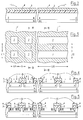
- FIG. 1 shows, in top-plan view, a semiconductor chip wherein two vertical MOS transistors 1', 1'' are integrated having different threshold voltages.
- Transistors of this type are generally formed by a plurality of polygonal elementary cells, both square and rectangular, or alternatively by a plurality of stripes. In the shown example, transistor 1' is formed by square cells, while transistor 1'' is formed by stripes.
- the process provides for epitaxial growth, on a semiconductor substrate 1 heavily doped of, e.g., the N type, of a generally lightly doped semiconductor layer 2 of the same conductivity type, forming together with substrate 1 the drain of transistors 1' and 1''.
- a gate oxide layer 3 and a polysilicon layer 4 are subsequently formed for creating respective gate electrodes 5 and 5' of transistors 1' and 1''.
- Electrodes 5, 5' are defined by means of a selective removal of layers 3 and 4, so as to define in layers 3, 4 openings that are square in the case of transistor 1', in form of stripes in the case of transistor 1'', as shown in Figure 3.
- a P type dopant is selectively introduced into the drain layer 2, using the gate electrodes 5, 5' as a mask, for the formation of body regions 7 of transistors 1' and 1''.
- the body regions 7 have the shape of squares and stripes, and extend under the gate electrodes 5, 5' to form the channel regions of the transistors.
- an N type dopant is selectively introduced in the body regions 7 to form source regions 8.
- the steps for forming the short-circuit between the body regions and the source regions, for realizing the insulation of the gate electrodes, for opening contacts, for forming metallization lines and for finally passivating the whole chip are performed in a conventional way.
- the threshold voltage of the MOS transistors is varied acting only on the geometry of the gate electrodes, which act as a mask for the selective introduction of the P type dopant.
- the dopant concentration in the channel region is lower than that at the rectilinear portions of the gate electrode (Darwish et al., "Transient Enhanced Threshold Shift in PWRMOS Transistors", IEDM).
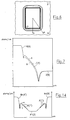
- the dopant concentration in the channel region near the corners of the gate electrode is lower than that near the rectilinear regions. In fact, near the corners there is a portion of greater volume for the dopant diffusion. Furthermore, the more the angle ⁇ formed by the corner of the gate electrode is acute, the lower the dopant concentration in the channel region.
- curve A in solid shows the surface dopant concentration profile in the channel region along a rectilinear portion of the gate electrode (direction a in Figure 6), while the dashed curve B shows the concentration profile in the channel region near the corner of the gate electrode (direction b in Figure 6).
- the peak dopant concentration in the channel region near gate electrodes comprising substantially rectilinear portions is higher than that in the channel region near the corners thereof.
- the peak dopant concentration depends on the geometry of the gate electrode, so that the threshold voltage of the vertical MOS transistor depends on the geometry of the gate electrode.
- each device thus exist two areas with different threshold voltages: the corners and the rectilinear regions.
- the operating threshold voltage of the device that driving voltage for which a prescribed current flows through the device, it follows that the operating threshold voltage depends on the corner density per unit area.
- the threshold voltage of those transistors having gate electrodes with a higher corner density per unity area is lower.
- the gate electrode of transistor 1' has, in the shown example, a corner density per unit area of:
- transistor 1' since transistor 1' has a higher corner density, it will conduct the prescribed current at a lower voltage applied to the gate electrode.
- FIG. 8 Further examples of layouts of vertical MOS transistors, wherein the gate electrodes have a stripe layout, are shown in Figures 8 and 9.
- the gate electrodes 30 of the transistors are stripes of constant width, but have a serpentine geometry.
- the body regions 60 take a rhomboidal shape, while in the embodiment of Figure 9 the body regions 60 have a serpentine geometry.
- source regions 70 are formed inside the body regions 60 so as to leave at least a central portion of the body regions for the contact of short-circuit to the source regions by means of a metallization layer.
- inventions allows to obtain extremely high corner densities per unit area, with the further advantage of varying continuously the angle ⁇ of the corners of the gate electrodes of the transistors integrated in the same chip.
- the angle ⁇ can be varied from a maximum of 180°, for which the gate electrode becomes a stripe substantially free of corners, to a minimum determined by optical resolution of the photolithographic equipment employed, to achieve the maximum corner density per unit area.
- Figures 10 to 13 show steps of a process according to the invention for the integration in a same chip of two horizontal MOS transistors with different threshold voltages.
- the shown embodiment provides for epitaxially growing, on a heavily doped semiconductor substrate 1 of, e.g., N type, a lightly doped semiconductor layer 2 of the same conductivity type.
- a lightly doped P- semiconductor layer 2' is formed, constituting the substrate of horizontal MOS transistors 9', 9''.
- An oxide layer 3 and a polysilicon layer 4 are then formed for creating the gate electrodes 10, 10'.
- the electrodes 10, 10' are defined by means of a selective removal of layers 3, 4.
- a P type dopant is selectively introduced in the substrate layer 2' using the gate electrodes 10, 10' as a mask, for the creation of P type regions 7' extending under the gate electrodes 10, 10'.
- an N type dopant is selectively introduced in the P type regions 7' for creating N+ source and drain regions 8'.
- the steps for the isolation of the gate electrode, for the opening of contacts, for the formation of metallization lines and for the final passivation of the whole chip are performed in a conventional way.
- the implant for the formation of the P type regions 7' in the P- well 2' of the horizontal MOS transistors is simultaneous with the formation of the body regions 7 of the vertical MOS transistors.
- the solid curve shows the dopant concentration profile along the channel region near a rectilinear gate electrode 10
- the dashed curve f shows the dopant concentration profile along the channel region near a corner of the gate electrode.
- the process according to the invention can be advantageously applied to horizontal transistors because, changing the density and the angle of aperture of the corners of the gate electrode it is possible to obtain transistors with different threshold voltages without additional process steps.
Landscapes
- Metal-Oxide And Bipolar Metal-Oxide Semiconductor Integrated Circuits (AREA)
- Insulated Gate Type Field-Effect Transistor (AREA)
Priority Applications (4)
| Application Number | Priority Date | Filing Date | Title |
|---|---|---|---|
| DE69734982T DE69734982D1 (de) | 1997-10-24 | 1997-10-24 | Verfahren zur Integration von MOS-Technologie-Bauelementen mit unterschiedlichen Schwellenspannungen in demselben Halbleiterchip |
| EP97830543A EP0915509B1 (de) | 1997-10-24 | 1997-10-24 | Verfahren zur Integration von MOS-Technologie-Bauelementen mit unterschiedlichen Schwellenspannungen in demselben Halbleiterchip |
| US09/178,369 US6040609A (en) | 1997-10-24 | 1998-10-23 | Process for integrating, in a single semiconductor chip, MOS technology devices with different threshold voltages |
| JP10303877A JPH11214529A (ja) | 1997-10-24 | 1998-10-26 | Mosデバイスの集積化方法及び半導体チイップ |
Applications Claiming Priority (1)
| Application Number | Priority Date | Filing Date | Title |
|---|---|---|---|
| EP97830543A EP0915509B1 (de) | 1997-10-24 | 1997-10-24 | Verfahren zur Integration von MOS-Technologie-Bauelementen mit unterschiedlichen Schwellenspannungen in demselben Halbleiterchip |
Publications (2)
| Publication Number | Publication Date |
|---|---|
| EP0915509A1 true EP0915509A1 (de) | 1999-05-12 |
| EP0915509B1 EP0915509B1 (de) | 2005-12-28 |
Family
ID=8230823
Family Applications (1)
| Application Number | Title | Priority Date | Filing Date |
|---|---|---|---|
| EP97830543A Expired - Lifetime EP0915509B1 (de) | 1997-10-24 | 1997-10-24 | Verfahren zur Integration von MOS-Technologie-Bauelementen mit unterschiedlichen Schwellenspannungen in demselben Halbleiterchip |
Country Status (4)
| Country | Link |
|---|---|
| US (1) | US6040609A (de) |
| EP (1) | EP0915509B1 (de) |
| JP (1) | JPH11214529A (de) |
| DE (1) | DE69734982D1 (de) |
Cited By (1)
| Publication number | Priority date | Publication date | Assignee | Title |
|---|---|---|---|---|
| WO2001031711A3 (en) * | 1999-10-22 | 2001-11-22 | Semiconductor Components Ind | Vertical insulated gate field-effect device and method of making the same |
Families Citing this family (15)
| Publication number | Priority date | Publication date | Assignee | Title |
|---|---|---|---|---|
| KR100251280B1 (ko) * | 1998-03-25 | 2000-04-15 | 윤종용 | 샐로우 트랜치 아이솔레이션 방법 |
| JP3209972B2 (ja) * | 1999-01-14 | 2001-09-17 | 沖電気工業株式会社 | 半導体集積回路装置 |
| JP2002246595A (ja) * | 2001-02-19 | 2002-08-30 | Shindengen Electric Mfg Co Ltd | トランジスタ |
| US7091565B2 (en) * | 2003-10-22 | 2006-08-15 | Marvell World Trade Ltd. | Efficient transistor structure |
| US7851872B2 (en) | 2003-10-22 | 2010-12-14 | Marvell World Trade Ltd. | Efficient transistor structure |
| US7960833B2 (en) | 2003-10-22 | 2011-06-14 | Marvell World Trade Ltd. | Integrated circuits and interconnect structure for integrated circuits |
| KR100582374B1 (ko) * | 2004-09-08 | 2006-05-22 | 매그나칩 반도체 유한회사 | 고전압 트랜지스터 및 그 제조 방법 |
| TWI390735B (zh) | 2005-01-28 | 2013-03-21 | 半導體能源研究所股份有限公司 | 半導體裝置,電子裝置,和半導體裝置的製造方法 |
| TWI505473B (zh) * | 2005-01-28 | 2015-10-21 | 半導體能源研究所股份有限公司 | 半導體裝置,電子裝置,和半導體裝置的製造方法 |
| US8416405B2 (en) * | 2008-08-08 | 2013-04-09 | Chemimage Corporation | Raman chemical imaging of implantable drug delivery devices |
| JP5769818B2 (ja) * | 2011-12-01 | 2015-08-26 | 三菱電機株式会社 | 半導体装置 |
| WO2013103051A1 (ja) * | 2012-01-06 | 2013-07-11 | 三菱電機株式会社 | 半導体装置 |
| US9818743B2 (en) * | 2013-06-21 | 2017-11-14 | Infineon Technologies Americas Corp. | Power semiconductor device with contiguous gate trenches and offset source trenches |
| US9673103B2 (en) | 2015-06-30 | 2017-06-06 | Stmicroelectronics, Inc. | MOSFET devices with asymmetric structural configurations introducing different electrical characteristics |
| US10665461B2 (en) | 2018-09-24 | 2020-05-26 | International Business Machines Corporation | Semiconductor device with multiple threshold voltages |
Citations (5)
| Publication number | Priority date | Publication date | Assignee | Title |
|---|---|---|---|---|
| US4941027A (en) * | 1984-06-15 | 1990-07-10 | Harris Corporation | High voltage MOS structure |
| EP0452817A1 (de) * | 1990-04-20 | 1991-10-23 | Kabushiki Kaisha Toshiba | Halbleiterbauelement mit MOS-Transistoren und Verfahren zu dessen Herstellung |
| EP0772242A1 (de) * | 1995-10-30 | 1997-05-07 | STMicroelectronics S.r.l. | Leistungsbauteil in MOS-Technologie mit einer einzelnen kritischen Grösse |
| US5635742A (en) * | 1994-02-02 | 1997-06-03 | Nissan Motor Co., Ltd. | Lateral double-diffused mosfet |
| EP0791965A2 (de) * | 1996-02-26 | 1997-08-27 | SILICONIX Incorporated | Vertikal-Transistor mit vier Klemmen |
Family Cites Families (11)
| Publication number | Priority date | Publication date | Assignee | Title |
|---|---|---|---|---|
| JP2968579B2 (ja) * | 1990-04-17 | 1999-10-25 | 三菱樹脂株式会社 | 固化押出板の成形方法 |
| US5132757A (en) * | 1990-11-16 | 1992-07-21 | Unisys Corporation | LDD field effect transistor having a large reproducible saturation current |
| JP2910489B2 (ja) * | 1993-03-22 | 1999-06-23 | 日本電気株式会社 | 縦型二重拡散mosfet |
| FR2705173B1 (fr) * | 1993-05-10 | 1995-07-28 | Sgs Thomson Microelectronics | Composant limiteur de courant serie. |
| JP3322738B2 (ja) * | 1993-12-08 | 2002-09-09 | 株式会社半導体エネルギー研究所 | 半導体装置及び集積回路ならびに表示装置 |
| US5757046A (en) * | 1994-01-07 | 1998-05-26 | Fuji Electric Company Ltd. | MOS type semiconductor device |
| JP3249007B2 (ja) * | 1994-03-17 | 2002-01-21 | 富士通株式会社 | 半導体装置、その特性評価方法及び設計方法 |
| US5796149A (en) * | 1994-09-09 | 1998-08-18 | Nippon Steel Corporation | Semiconductor memory using different concentration impurity diffused layers |
| JP4059939B2 (ja) * | 1996-08-23 | 2008-03-12 | 株式会社半導体エネルギー研究所 | パワーmosデバイス及びその作製方法 |
| US5900666A (en) * | 1996-12-03 | 1999-05-04 | Advanced Micro Devices, Inc. | Ultra-short transistor fabrication scheme for enhanced reliability |
| US5965925A (en) * | 1997-10-22 | 1999-10-12 | Artisan Components, Inc. | Integrated circuit layout methods and layout structures |
-
1997
- 1997-10-24 DE DE69734982T patent/DE69734982D1/de not_active Expired - Lifetime
- 1997-10-24 EP EP97830543A patent/EP0915509B1/de not_active Expired - Lifetime
-
1998
- 1998-10-23 US US09/178,369 patent/US6040609A/en not_active Expired - Lifetime
- 1998-10-26 JP JP10303877A patent/JPH11214529A/ja active Pending
Patent Citations (5)
| Publication number | Priority date | Publication date | Assignee | Title |
|---|---|---|---|---|
| US4941027A (en) * | 1984-06-15 | 1990-07-10 | Harris Corporation | High voltage MOS structure |
| EP0452817A1 (de) * | 1990-04-20 | 1991-10-23 | Kabushiki Kaisha Toshiba | Halbleiterbauelement mit MOS-Transistoren und Verfahren zu dessen Herstellung |
| US5635742A (en) * | 1994-02-02 | 1997-06-03 | Nissan Motor Co., Ltd. | Lateral double-diffused mosfet |
| EP0772242A1 (de) * | 1995-10-30 | 1997-05-07 | STMicroelectronics S.r.l. | Leistungsbauteil in MOS-Technologie mit einer einzelnen kritischen Grösse |
| EP0791965A2 (de) * | 1996-02-26 | 1997-08-27 | SILICONIX Incorporated | Vertikal-Transistor mit vier Klemmen |
Cited By (2)
| Publication number | Priority date | Publication date | Assignee | Title |
|---|---|---|---|---|
| WO2001031711A3 (en) * | 1999-10-22 | 2001-11-22 | Semiconductor Components Ind | Vertical insulated gate field-effect device and method of making the same |
| US6344379B1 (en) | 1999-10-22 | 2002-02-05 | Semiconductor Components Industries Llc | Semiconductor device with an undulating base region and method therefor |
Also Published As
| Publication number | Publication date |
|---|---|
| JPH11214529A (ja) | 1999-08-06 |
| US6040609A (en) | 2000-03-21 |
| DE69734982D1 (de) | 2006-02-02 |
| EP0915509B1 (de) | 2005-12-28 |
Similar Documents
| Publication | Publication Date | Title |
|---|---|---|
| US5391506A (en) | Manufacturing method for semiconductor devices with source/drain formed in substrate projection. | |
| US6617656B2 (en) | EDMOS device having a lattice type drift region | |
| US6461920B1 (en) | Semiconductor device and method of manufacturing the same | |
| US5510279A (en) | Method of fabricating an asymmetric lightly doped drain transistor device | |
| US5879994A (en) | Self-aligned method of fabricating terrace gate DMOS transistor | |
| EP0772242B1 (de) | Leistungsbauteil in MOS-Technologie mit einer einzelnen kritischen Grösse | |
| EP0915509B1 (de) | Verfahren zur Integration von MOS-Technologie-Bauelementen mit unterschiedlichen Schwellenspannungen in demselben Halbleiterchip | |
| US7550352B2 (en) | MOS transistor having a recessed gate electrode and fabrication method thereof | |
| US5016067A (en) | Vertical MOS transistor | |
| US5945710A (en) | Semiconductor device with doped contact impurity regions having particular doping levels | |
| US5721148A (en) | Method for manufacturing MOS type semiconductor device | |
| KR910002037B1 (ko) | 반도체장치 및 그 제조방법 | |
| EP0772241B1 (de) | Leistungsbauteil hoher Dichte in MOS-Technologie | |
| US6608336B2 (en) | Lateral double diffused MOS transistor | |
| US5623154A (en) | Semiconductor device having triple diffusion | |
| US6294803B1 (en) | Semiconductor device having trench with vertically formed field oxide | |
| KR0159141B1 (ko) | 다수의 불순물층을 포함하고 있는 반도체장치 및 그 제조방법 | |
| JP4631097B2 (ja) | 所望のドーパント濃度を実現するためのイオン注入法 | |
| JPH09293865A (ja) | 半導体装置及び半導体製造方法 | |
| KR0138234B1 (ko) | 고전압 모오스 트랜지스터의 구조 | |
| KR100505271B1 (ko) | 엠오에스-게이트반도체소자 | |
| JP2924947B2 (ja) | 半導体装置の製造方法 | |
| EP0899785A2 (de) | Herstellungsverfahren für DRAM-Zelleanordnung | |
| US20070096245A1 (en) | Semiconductor device and manufacturing method for the same | |
| JPH05218416A (ja) | 半導体装置の製造方法 |
Legal Events
| Date | Code | Title | Description |
|---|---|---|---|
| PUAI | Public reference made under article 153(3) epc to a published international application that has entered the european phase |
Free format text: ORIGINAL CODE: 0009012 |
|
| AK | Designated contracting states |
Kind code of ref document: A1 Designated state(s): DE FR GB IT |
|
| AX | Request for extension of the european patent |
Free format text: AL;LT;LV;RO;SI |
|
| 17P | Request for examination filed |
Effective date: 19991026 |
|
| AKX | Designation fees paid |
Free format text: DE FR GB IT |
|
| 17Q | First examination report despatched |
Effective date: 20040816 |
|
| GRAP | Despatch of communication of intention to grant a patent |
Free format text: ORIGINAL CODE: EPIDOSNIGR1 |
|
| GRAS | Grant fee paid |
Free format text: ORIGINAL CODE: EPIDOSNIGR3 |
|
| GRAA | (expected) grant |
Free format text: ORIGINAL CODE: 0009210 |
|
| AK | Designated contracting states |
Kind code of ref document: B1 Designated state(s): DE FR GB IT |
|
| PG25 | Lapsed in a contracting state [announced via postgrant information from national office to epo] |
Ref country code: IT Free format text: LAPSE BECAUSE OF FAILURE TO SUBMIT A TRANSLATION OF THE DESCRIPTION OR TO PAY THE FEE WITHIN THE PRESCRIBED TIME-LIMIT;WARNING: LAPSES OF ITALIAN PATENTS WITH EFFECTIVE DATE BEFORE 2007 MAY HAVE OCCURRED AT ANY TIME BEFORE 2007. THE CORRECT EFFECTIVE DATE MAY BE DIFFERENT FROM THE ONE RECORDED. Effective date: 20051228 |
|
| REG | Reference to a national code |
Ref country code: GB Ref legal event code: FG4D |
|
| REF | Corresponds to: |
Ref document number: 69734982 Country of ref document: DE Date of ref document: 20060202 Kind code of ref document: P |
|
| PG25 | Lapsed in a contracting state [announced via postgrant information from national office to epo] |
Ref country code: DE Free format text: LAPSE BECAUSE OF FAILURE TO SUBMIT A TRANSLATION OF THE DESCRIPTION OR TO PAY THE FEE WITHIN THE PRESCRIBED TIME-LIMIT Effective date: 20060329 |
|
| ET | Fr: translation filed | ||
| PGFP | Annual fee paid to national office [announced via postgrant information from national office to epo] |
Ref country code: IT Payment date: 20061031 Year of fee payment: 10 |
|
| PLBE | No opposition filed within time limit |
Free format text: ORIGINAL CODE: 0009261 |
|
| STAA | Information on the status of an ep patent application or granted ep patent |
Free format text: STATUS: NO OPPOSITION FILED WITHIN TIME LIMIT |
|
| 26N | No opposition filed |
Effective date: 20060929 |
|
| PG25 | Lapsed in a contracting state [announced via postgrant information from national office to epo] |
Ref country code: IT Free format text: LAPSE BECAUSE OF NON-PAYMENT OF DUE FEES Effective date: 20071024 |
|
| PGFP | Annual fee paid to national office [announced via postgrant information from national office to epo] |
Ref country code: GB Payment date: 20110926 Year of fee payment: 15 |
|
| GBPC | Gb: european patent ceased through non-payment of renewal fee |
Effective date: 20121024 |
|
| PG25 | Lapsed in a contracting state [announced via postgrant information from national office to epo] |
Ref country code: GB Free format text: LAPSE BECAUSE OF NON-PAYMENT OF DUE FEES Effective date: 20121024 |
|
| PGFP | Annual fee paid to national office [announced via postgrant information from national office to epo] |
Ref country code: FR Payment date: 20131028 Year of fee payment: 17 |
|
| REG | Reference to a national code |
Ref country code: FR Ref legal event code: ST Effective date: 20150630 |
|
| PG25 | Lapsed in a contracting state [announced via postgrant information from national office to epo] |
Ref country code: FR Free format text: LAPSE BECAUSE OF NON-PAYMENT OF DUE FEES Effective date: 20141031 |