EP0915568A2 - Phasenregelkreis - Google Patents
Phasenregelkreis Download PDFInfo
- Publication number
- EP0915568A2 EP0915568A2 EP98120641A EP98120641A EP0915568A2 EP 0915568 A2 EP0915568 A2 EP 0915568A2 EP 98120641 A EP98120641 A EP 98120641A EP 98120641 A EP98120641 A EP 98120641A EP 0915568 A2 EP0915568 A2 EP 0915568A2
- Authority
- EP
- European Patent Office
- Prior art keywords
- oscillator
- circuit
- signal
- characteristic
- frequency
- Prior art date
- Legal status (The legal status is an assumption and is not a legal conclusion. Google has not performed a legal analysis and makes no representation as to the accuracy of the status listed.)
- Granted
Links
- 238000010586 diagram Methods 0.000 description 19
- 238000000034 method Methods 0.000 description 13
- 230000008569 process Effects 0.000 description 12
- 230000006399 behavior Effects 0.000 description 8
- 230000035945 sensitivity Effects 0.000 description 7
- 230000000694 effects Effects 0.000 description 5
- 230000009471 action Effects 0.000 description 4
- 230000008859 change Effects 0.000 description 4
- 230000000295 complement effect Effects 0.000 description 4
- 230000010354 integration Effects 0.000 description 4
- 230000004913 activation Effects 0.000 description 3
- 230000006978 adaptation Effects 0.000 description 3
- 238000004519 manufacturing process Methods 0.000 description 3
- 230000008901 benefit Effects 0.000 description 2
- 230000015572 biosynthetic process Effects 0.000 description 2
- 238000010276 construction Methods 0.000 description 2
- 238000005516 engineering process Methods 0.000 description 2
- 230000000630 rising effect Effects 0.000 description 2
- 238000003786 synthesis reaction Methods 0.000 description 2
- 230000007704 transition Effects 0.000 description 2
- 238000011144 upstream manufacturing Methods 0.000 description 2
- 238000013016 damping Methods 0.000 description 1
- 230000001934 delay Effects 0.000 description 1
- 238000006073 displacement reaction Methods 0.000 description 1
- 238000001914 filtration Methods 0.000 description 1
- 230000009467 reduction Effects 0.000 description 1
- 230000000717 retained effect Effects 0.000 description 1
- 230000001360 synchronised effect Effects 0.000 description 1
Images


Classifications
-
- H—ELECTRICITY
- H03—ELECTRONIC CIRCUITRY
- H03L—AUTOMATIC CONTROL, STARTING, SYNCHRONISATION OR STABILISATION OF GENERATORS OF ELECTRONIC OSCILLATIONS OR PULSES
- H03L7/00—Automatic control of frequency or phase; Synchronisation
- H03L7/06—Automatic control of frequency or phase; Synchronisation using a reference signal applied to a frequency- or phase-locked loop
- H03L7/08—Details of the phase-locked loop
- H03L7/099—Details of the phase-locked loop concerning mainly the controlled oscillator of the loop
-
- H—ELECTRICITY
- H03—ELECTRONIC CIRCUITRY
- H03L—AUTOMATIC CONTROL, STARTING, SYNCHRONISATION OR STABILISATION OF GENERATORS OF ELECTRONIC OSCILLATIONS OR PULSES
- H03L7/00—Automatic control of frequency or phase; Synchronisation
- H03L7/06—Automatic control of frequency or phase; Synchronisation using a reference signal applied to a frequency- or phase-locked loop
- H03L7/08—Details of the phase-locked loop
- H03L7/10—Details of the phase-locked loop for assuring initial synchronisation or for broadening the capture range
- H03L7/101—Details of the phase-locked loop for assuring initial synchronisation or for broadening the capture range using an additional control signal to the controlled loop oscillator derived from a signal generated in the loop
- H03L7/102—Details of the phase-locked loop for assuring initial synchronisation or for broadening the capture range using an additional control signal to the controlled loop oscillator derived from a signal generated in the loop the additional signal being directly applied to the controlled loop oscillator
-
- H—ELECTRICITY
- H04—ELECTRIC COMMUNICATION TECHNIQUE
- H04L—TRANSMISSION OF DIGITAL INFORMATION, e.g. TELEGRAPHIC COMMUNICATION
- H04L7/00—Arrangements for synchronising receiver with transmitter
- H04L7/02—Speed or phase control by the received code signals, the signals containing no special synchronisation information
- H04L7/033—Speed or phase control by the received code signals, the signals containing no special synchronisation information using the transitions of the received signal to control the phase of the synchronising-signal-generating means, e.g. using a phase-locked loop
Definitions
- the present invention relates to a phase locked loop (PLL) circuit according to the preamble of claim 1.
- PLL phase locked loop
- PLL's have been originally devised to solve the problem of locking the phase of the carrier in a receiver and they have subsequently found employ in the most diverse sectors, such as frequency synthesis, in its various applications, or automatic controls.
- the present invention was developed by paying particular attention to the need to obtain a PLL characterised by a low jitter value and suited to find application in fast clock distribution within integrated circuits or printed circuit boards, or, more in general, in applications that require frequency synthesis.
- the invention arose from activities aimed at obtaining a PLL destined to accomplish phase locking and/or frequency locking and multiplication on a clock signal, for instance for SDH (Synchronous Digital Hierarchy) applications, and having the following characteristics:
- PLL's include an input phase (and possibly frequency) comparator stage, followed by a so-called loop filter (usually a low-pass filter) and then by an oscillator (usually a Voltage Controlled Oscillator or VCO).
- a so-called loop filter usually a low-pass filter
- an oscillator usually a Voltage Controlled Oscillator or VCO
- the output signal deduced or derived from the output of the oscillator is fed back to the input of the input comparator stage through a feedback loop.
- the presence of frequency divider circuits, for instance, in the feedback loop allows making the circuit operate as a frequency multiplier circuit.
- the presence of divider circuits upstream of the comparator allows extending the frequency multiplication function to output frequency/input frequency ratios other than a whole number:
- a loop structure usually needs to be used, since it is not practically possible to use an LC oscillator due to the well known limitations inherent to the manufacture of inductors at the integrated circuit level, particularly for CMOS technology which is commonly used in the applications envisioned for the invention.
- the need to construct the loop filter as a part of the integrated circuit also compels, for construction reasons, to use small capacitance values with respect to the values that are suited for its manufacture as a circuit with discrete components.
- Another possibly critical factor stems from the need to make a judicious choice of the cut-off frequency in the jitter transfer function, which ideally should be chosen as low as possible in order to boost the jitter reduction effect by the filter.
- the latter need in fact is in contrast with the impossibility of obtaining high capacitance values of the filter.
- the problem tackled by the invention therefore is that of obtaining a PLL that is capable of meeting the operating requirements described above whilst still taking into account the intrinsic limitations recalled.
- the solution according to the invention offers the possibility of choosing the operating characteristic of the oscillator, with the consequent possibility of lowering the value of the sensitivity (Ko) of the oscillator itself, and of maintaining such sensitivity essentially constant with variations in quantities such as, for instance, temperature, power supply voltage and the parameters of the integration process.
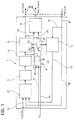
- reference 1 indicates in its entirety a PLL circuit which, according to a configuration known in itself, comprises the following elements or modules:
- control module 8 has been shown here as being ideally subdivided into two parts, indicated as 80 and 81 respectively.
- the term "control module” will also be used to indicate each of the two parts.
- the part 80 performs the normal function of controlling the operation of the PLL, in particular by intervening on the oscillator 5 as well as on dividers 6 and 7 according to a configuration signal Cl coming from outside through a line 13.
- the references 20, 21 and 22 show three lines through which the control module 80 acts, respectively, on the oscillator 5, on the first divider 6 and on the second divider 7.
- the part 81 instead is specifically dedicated to controlling the operation of the oscillator 5, through a line 200.
- CLKIN The clock signal for which the phase lock and/or frequency lock and multiplication functions are to be performed according to the embodiment described herein has been denoted CLKIN.
- This signal is carried through a line 10 to the input of the comparator 2 and, through a line 11, to one of the inputs of the control module 81.
- the latter also receives, through a second line 12, a driving signal related with the output of the comparator 2, in particular the output signal of the loop filter 4.
- This choice is anyway not to be taken as mandatory: an essentially similar function could be performed, for instance, by the output of the current pump 3.
- driving the control module 81 starting from the output of the loop filter 4 is found advantageous because this allows taking advantage of the filtering action of the filter 4 itself.
- the output signal CLKOUT of the oscillator 5 constitutes the output signal of the circuit, present on a line 14.
- the same signal is also sent, through a line 15, to the divider 6 which derives therefrom a frequency-divided output signal DCLKOUT, present on a line 16.
- a feedback signal FBLCK, present on a line 17, is fed back towards the comparator 2 both through a direct line 18 and through a secondary line 19 which passes through the second divider 7.
- FBLCK feedback signal
- the feedback action towards comparator 2 can therefore be effected both starting from the output signal CLKOUT present on the line 14 and starting from the frequency-divided signal DCLKOUT present on the line 16, as well as from any other element positioned downstream of the lines 14 and 16.
- This choice can be found advantageous to take into account, for instance, additional phase displacements that may be induced by those downstream elements. In any case this is a preferential and not mandatory choice and, in the remainder of the present description, it may ideally be imagined that the feedback line 17 is simply closed on the output line 14 as schematically shown in Fig. 1 with a dashed line.
- both dividers 6, 7 whose function is to generate the frequency divided output signal DCLKOUT and, respectively, to allow the frequency multiplication.
- the splitting of the feedback path into the two lines 18, 19 is destined to account for the fact that, in essential analogy with what has been stated above in regard to the output of the circuit 1, the divider 7 may introduce in the feedback loop delays that cannot be exactly determined.
- the circuit 1 can be activated initially by making the comparator 2 exploit, as feedback line, the "direct" line 18, thereby allowing the desired locking conditions to be reached in the circuit.
- the comparator 2 can then take into account the signal present on the line 19 wherein the divider 7 is inserted. This allows the latter to perform its function (in practice, in the form of a "decimation" of order N of the pulses comprising its input signal) without modifying the lock conditions set by using the direct line 18.
- a preferred characteristic of the circuit 1 is the use of a differential structure at least for the current pump 3, the loop filter 4 and the oscillator 5.
- the term differential structure is meant to indicate in general a structure wherein the signal transferred from one element to another actually comprises the difference between the signal values (typically voltage values) present on two complementary lines, respectively positive and negative (or inverting). This choice offers, among other factors, the advantage of offering a lesser sensitivity to noise, in particular to noise on the power supply, also giving rise to a lesser generation of disturbances (for it is possible to work with smaller and complementary signals, with circuits that operate in linear zone).
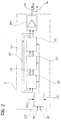
- FIG. 2 shows in greater detail the structure of the oscillator 5, constructed, as stated above, according to the typical configuration of a Voltage Controlled Oscillator or VCO.
- the structure is known in itself, but it is shown to ease understanding of the invention.
- the oscillator 5 comprises three delay elements or stages 23 connected in cascade:
- the drawing clearly shows the complementary structure of the respective connecting lines 24 as well as of the feedback line 25 which connects (in an inverting manner, i. e. by creating a negative feedback) the output of the delay element 23 farthest downstream with the input of the element located farthest upstream.
- the reference 26 indicates an output buffer circuit which acts on the output signal of the element 23 farthest downstream thereby making it suitable for being sent on the line 14 (and on the line 15, if present).
- the reference 27 indicates a control circuit that receives at its input (preferably in complementary configuration, through two lines indicated respectively as 40 and 41) the output signal of the loop filter 4.
- the circuit 27 further requires, as configuration control signals, the signals incoming on the lines 20 and 200.
- the oscillator diagram shown in Fig. 2 provides for frequency control to be effected by varying the output impedance of the individual stage (or element) 23, also aiming at obtaining a constant voltage range at the output of the individual stage.
- the related control procedures starting from module 27 essentially correspond to those described for instance in the work "Fully Integrated CMOS Phase-Locked Loop with 15 to 240 MHz Locking Range and ⁇ 50 ps jitter" by Ilya Novof et al., in ISSCC Dig. Tech. Papers, February 1995, pages 112 - 113.
- the control module 80 acts on the module 27 through the input 20 in the way described in the aforementioned work by Novof et al., in particular with reference to Fig. 7, thereby allowing constructing the filter 4 as an essentially capacitive component, and also controlling the damping of the circuit according to the division factors of the dividers 6 and 7.
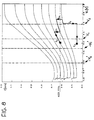
- the control module 81 acts on the module 27 through the input 200 in such a way that the VCO operates according to one among several frequency/voltage characteristics as shown schematically in the diagrams of Figs. 3A - 3C.
- fast parameters and “slow parameters” have been used since the variability of the results of the technological process translates in practice into a higher or lower operating speed of the component.
- each condition there is a family of characteristics (eight in the embodiment shown).
- the various characteristics in each family correspond to a different configuration whereby the oscillator 5 is driven by the circuit 27, i. e. to a number of different behaviours of the output frequency versus the input voltage for different values of the logic combination applied on the line 200.
- the lowermost characteristic in Figs. 3A - 3C corresponds to an input logic combination "000" on the line 200, whereas the uppermost characteristic corresponds to a different combination, such as "111".
- the described embodiment may be implemented by using a greater or smaller number of characteristics or yet again, at least theoretically, with the possibility of choosing the individual characteristic adopted within a range that is no longer discrete (as in the case of the embodiment shown) but continuous or essentially continuous.
- the parameters represented by the characteristics highlighted above may be critical for the correct operation of the device.
- ⁇ n 2Kd ⁇ Ko NC
- ⁇ n the pulsatance in question
- C the capacitance value corresponding to the behaviour of the filter 4
- Kd and Ko are the sensitivities of the comparator 2 and of the oscillator 5.
- Formula (I) allows understanding that the impossibility of implemented high values of capacitance C compels to keep low the value of the product KdKo in order to keep the value of the pulsatance ⁇ n limited.
- pulsatance In practice, for the frequency values indicated in the introductory part of the specification, it is preferred for that pulsatance to remain at values corresponding to frequencies in the order of 1 - 2 MHz.
- Value Kd indicative of the sensitivity of the comparator 2, cannot decrease below a certain value because of the need to prevent the signal itself from being excessively penalised by noise.
- a PLL essentially similar to circuit 1 described here, wherein however the VCO 5 presents a single operating characteristic, for instance the uppermost characteristic in the three diagrams in Figs. 3A - 3C, could be overall acceptable in the case of operation at 80° C (Fig. 3A). However, it would be wholly unacceptable (because it would correspond to an excessively high value of gain) in the case of operation at 0° C (observe the uppermost curve in the diagram in Fig. 3C).
- an oscillator 5 with variable characteristic in particular with the possibility of being made to operate according to a frequency/voltage characteristic selectively identified within a range of available characteristics, allows optimising the operation of the circuit: by adapting the behaviour of the oscillator 5 to the specific conditions (temperature, power supply voltage, process parameters).
- the control module 81 intervene on the oscillator 5 to make it operate with the characteristic corresponding to the third curve from the bottom in the diagram in Fig. 3B.
- the same module 81 can intervene on the oscillator 5 in such a way as to make it operate according to a characteristic corresponding to the sixth curve starting from the bottom in the diagram in Fig. 3A.
- the same module 81 can intervene on the oscillator 5 in such a way as to make it operate according to the characteristic 1, i. e. the lowest one in the diagram in Fig. 3C.
- the adaptation of the operation of the oscillator 5 can be effected, as a function of the working frequency, as a veritable calibration action effected on the circuit.
- the circuit manufactured, (for instance in the form of an integrated circuit) its operation can be adjusted according to the conditions of use in such a way as to optimise its behaviour for instance, as a function of the process parameters (generally not controllable a priori ).
- Figs. 4 and 7 refer to a preferred embodiment where such adjustment becomes an automatic adaptation function.
- the circuit can thus be configured in such a way that, upon activation, it is able to place itself automatically on the operating characteristic of the oscillator 5 that corresponds to the desired optimal conditions, with the possibility of subsequently choosing another characteristic when the one adopted previously is no longer to be considered optimal.
- the transition of the oscillator 5 from one operating characteristic to another may constitute an undesired phenomenon, as it may give rise, for instance, to a "jump" of one period in the clock signal.
- the oscillator 5 it seems therefore preferable, once a given characteristic is adopted upon circuit activation, for the oscillator 5 to be maintained on that operating characteristic even when it has become sub-optimal, except in presence of important phenomena (for instance a strong variation in the input frequency of the device), such as to make the adopted characteristic so unsatisfactory that the onset of a negative phenomenon like the jump of one synchronisation period is nevertheless preferable to continuing operation on a characteristic that has become sub-optimal.
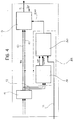
- FIGs in Figs. 4 and 6 show, together with Fig. 8, the possible embodiment of such a function of automatic tracking of the optimal characteristic followed by a function of permanence on such characteristics so as to prevent, or in any case to make very improbable (except in case of a radical change in the operating conditions of the device), further characteristic changes.
- the aforesaid function is driven by the output signal of the loop filter 4 (line 12 of Fig. 1, shown in the diagram in Fig. 4 in its differential configuration).
- the reference 30 indicates a configuration control circuit whose output essentially corresponds to the line 200.
- the circuit 30 allows making the VCO 5 operate according to a characteristic selectively determined.
- the circuit 30 operates when enabled by the input clock CLKIN present on the line 11 and under the control of two signals, respectively defined as rising (UP) signal and falling (DOWN) signal: the sense of "up” and “down” is taken here as the one corresponding to the order according to which the characteristics are presented in the various diagrams in the Figures 3A - 3C.
- the UP signal determines such an intervention of the configuration control circuit 30 as to lead the oscillator 5 to operate on a higher characteristic than the one where it is currently located.
- the DOWN signal determines an intervention in the opposite direction.
- the DOWN and UP signals are produced by a comparator circuit 31 essentially consisting in a double comparator with hysteresis having the characteristics shown in Figs. 5A and 5B.
- the values of the differential input signal V c present on the lines 12 are plotted in the x-axes.
- the y-axes correspond instead to the UP signal (in Fig. 5A) and to the DOWN signal (in Fig. 5B).
- the "high” value corresponds, in both Figures, to the active state of the related signal, with consequent change in the operating characteristic of the oscillator 5.
- the "low” value corresponds instead to the absence of output signal. In practice, when both output signals are at the "low” value, the operating characteristic of the oscillator 5 is retained unaltered.
- the circuit 30 essentially consists in a state machine 301 which reads the UP and DOWN signals at the instants identified by a clock signal generated internally, by means of a divider 302, starting from the signal CLKIN present on the line 11, and in a decoder 303 that converts the states of the machine 301 into logic signals suitable for driving the block 27.
- the state diagram of state machine 301 and the related transitions are shown in Fig. 7.
- Fig. 8 refers, for the sake of simplicity and clarity of illustration, to the family of operating characteristics shown in Fig. 3B and shows the two pairs of threshold values V 1 , V 2 and -V 1 ', -V 2 ' of the comparator 31.
- the circuit 31 emits the UP signal and, in correspondence with the subsequent rising front of CLKIN, the state machine passes to state 1, thereby selecting the first characteristic. Underthose conditions, the operating frequency of the oscillator 5 increases rapidly as is illustrated schematically by the arrow t 1 .
- the operating frequency of the oscillator Upon reaching the cross-over point between the voltage value V 2 and the first characteristic, the operating frequency of the oscillator is still lower than the desired value of 622 MHz and consequently the UP signal is still active. As a result thereof, although it has performed its function of tracking the desired frequency on the first characteristic, the comparator 31 intervenes (UP signal) on the configuration control element 30 thereby causing the oscillator to operate on the second characteristic, as shown in t 2 at the right-hand side of Fig. 8 (passage to state 2).
- the oscillator 5 moves to the desired operating point (arrow t 4 ), which as shown corresponds to an input voltage lower than V 1 and to an output frequency equal to the desired frequency of 622 MHz.
- the UP signal is at a low level and the circuit becomes stabilised in the aforesaid operating condition, remaining there even in the presence of rather marked changes in the behaviour of the VCO 5, due for instance to temperature variations, provided - however - that such changes do not cause the oscillator 5 to depart from the central band comprised between the extreme switching levels (V 2 , -V 2 ') of the comparator with hysteresis 31.
- the control voltage exceeds V 2 or drops below -V 2 ' and a new characteristic is chosen as described above.
- the result is the generation, by the circuit 31, of the UP or DOWN signal so as to cause, through the configuration control module 30, the oscillator 5, to move to the desired characteristic.
Landscapes
- Engineering & Computer Science (AREA)
- Computer Networks & Wireless Communication (AREA)
- Signal Processing (AREA)
- Stabilization Of Oscillater, Synchronisation, Frequency Synthesizers (AREA)
- Manipulation Of Pulses (AREA)
Applications Claiming Priority (2)
| Application Number | Priority Date | Filing Date | Title |
|---|---|---|---|
| IT97TO000970A IT1295950B1 (it) | 1997-11-06 | 1997-11-06 | Circuito ad aggancio di fase. |
| ITTO970970 | 1997-11-06 |
Publications (3)
| Publication Number | Publication Date |
|---|---|
| EP0915568A2 true EP0915568A2 (de) | 1999-05-12 |
| EP0915568A3 EP0915568A3 (de) | 2000-07-19 |
| EP0915568B1 EP0915568B1 (de) | 2004-05-26 |
Family
ID=11416118
Family Applications (1)
| Application Number | Title | Priority Date | Filing Date |
|---|---|---|---|
| EP98120641A Expired - Lifetime EP0915568B1 (de) | 1997-11-06 | 1998-11-03 | Phasenregelkreis und Verfahren zum Steuern des Phasenregelkreises |
Country Status (6)
| Country | Link |
|---|---|
| US (1) | US6127896A (de) |
| EP (1) | EP0915568B1 (de) |
| JP (1) | JPH11225070A (de) |
| CA (1) | CA2253583C (de) |
| DE (1) | DE69824114T2 (de) |
| IT (1) | IT1295950B1 (de) |
Cited By (1)
| Publication number | Priority date | Publication date | Assignee | Title |
|---|---|---|---|---|
| US6259327B1 (en) * | 1998-12-11 | 2001-07-10 | Cselt - Centro Studi E Laboratori Telecomunicazioni S.P.A. | PLL having circuits for selecting optimum VCO input/output characteristics |
Families Citing this family (12)
| Publication number | Priority date | Publication date | Assignee | Title |
|---|---|---|---|---|
| JP3573975B2 (ja) * | 1998-10-23 | 2004-10-06 | 日本オプネクスト株式会社 | 光受信器、位相同期ループ回路、電圧制御発振器および周波数応答可変増幅器 |
| US6674331B2 (en) | 2001-11-09 | 2004-01-06 | Agere Systems, Inc. | Method and apparatus for simplified tuning of a two-point modulated PLL |
| US7187220B1 (en) * | 2003-12-18 | 2007-03-06 | Nvidia Corporation | Memory clock slowdown |
| US7315957B1 (en) | 2003-12-18 | 2008-01-01 | Nvidia Corporation | Method of providing a second clock while changing a first supplied clock frequency then supplying the changed first clock |
| JP4651298B2 (ja) * | 2004-04-08 | 2011-03-16 | 三菱電機株式会社 | 周波数自動補正pll回路 |
| DE102004032130B4 (de) * | 2004-07-01 | 2010-12-16 | Krohne Messtechnik Gmbh | Frequenzsynthesizer und Verfahren zum Betrieb eines Frequenzsynthesizers |
| TWI296464B (en) * | 2005-06-20 | 2008-05-01 | Airoha Tech Corp | Phase lock loop and operating method thereof |
| US9262837B2 (en) | 2005-10-17 | 2016-02-16 | Nvidia Corporation | PCIE clock rate stepping for graphics and platform processors |
| US7671642B2 (en) * | 2006-12-13 | 2010-03-02 | Atmel Corporation | Amplitude controlled sawtooth generator |
| US7336110B1 (en) | 2007-01-17 | 2008-02-26 | Atmel Corporation | Differential amplitude controlled sawtooth generator |
| US20090153252A1 (en) * | 2007-12-13 | 2009-06-18 | Mei-Show Chen | Multi-band voltage controlled oscillator controlling module, phase locked loop utilizing which and related method thereof |
| US7834708B1 (en) * | 2008-04-30 | 2010-11-16 | Integrated Device Technology, Inc. | Method and apparatus for analog smooth switch in VCO loading control |
Family Cites Families (6)
| Publication number | Priority date | Publication date | Assignee | Title |
|---|---|---|---|---|
| JPH0799807B2 (ja) * | 1990-03-09 | 1995-10-25 | 株式会社東芝 | 位相同期回路 |
| DE4031939A1 (de) * | 1990-10-09 | 1992-05-07 | Rohde & Schwarz | Verfahren zum voreinstellen eines phasengeregelten oszillators auf einen vorgegebenen frequenzwert |
| US5257294A (en) * | 1990-11-13 | 1993-10-26 | National Semiconductor Corporation | Phase-locked loop circuit and method |
| KR940005459A (ko) * | 1992-06-22 | 1994-03-21 | 모리시타 요이찌 | Pll회로 |
| US5331292A (en) * | 1992-07-16 | 1994-07-19 | National Semiconductor Corporation | Autoranging phase-lock-loop circuit |
| US5422603A (en) * | 1994-06-02 | 1995-06-06 | International Business Machines Corporation | CMOS frequency synthesizer |
-
1997
- 1997-11-06 IT IT97TO000970A patent/IT1295950B1/it active IP Right Grant
-
1998
- 1998-09-18 US US09/156,930 patent/US6127896A/en not_active Expired - Lifetime
- 1998-10-30 JP JP10324400A patent/JPH11225070A/ja active Pending
- 1998-11-03 DE DE69824114T patent/DE69824114T2/de not_active Expired - Lifetime
- 1998-11-03 EP EP98120641A patent/EP0915568B1/de not_active Expired - Lifetime
- 1998-11-04 CA CA002253583A patent/CA2253583C/en not_active Expired - Fee Related
Cited By (1)
| Publication number | Priority date | Publication date | Assignee | Title |
|---|---|---|---|---|
| US6259327B1 (en) * | 1998-12-11 | 2001-07-10 | Cselt - Centro Studi E Laboratori Telecomunicazioni S.P.A. | PLL having circuits for selecting optimum VCO input/output characteristics |
Also Published As
| Publication number | Publication date |
|---|---|
| CA2253583C (en) | 2001-05-15 |
| IT1295950B1 (it) | 1999-05-28 |
| EP0915568A3 (de) | 2000-07-19 |
| EP0915568B1 (de) | 2004-05-26 |
| ITTO970970A1 (it) | 1999-05-06 |
| JPH11225070A (ja) | 1999-08-17 |
| DE69824114D1 (de) | 2004-07-01 |
| ITTO970970A0 (it) | 1997-11-06 |
| DE69824114T2 (de) | 2005-07-07 |
| US6127896A (en) | 2000-10-03 |
| CA2253583A1 (en) | 1999-05-06 |
Similar Documents
| Publication | Publication Date | Title |
|---|---|---|
| US6259327B1 (en) | PLL having circuits for selecting optimum VCO input/output characteristics | |
| EP0915568B1 (de) | Phasenregelkreis und Verfahren zum Steuern des Phasenregelkreises | |
| US5548235A (en) | Phase-locked loop and resulting frequency multiplier | |
| EP0482823B1 (de) | Frequenzsynthesierer mit PLL, der einen Frequenzwechsel des Ausgangs mit hoher Geschwindigkeit ermöglicht | |
| EP1933464B1 (de) | Phasenregelkreis mit adaptiver Bandbreite und Vorkopplungsteiler | |
| US6747519B2 (en) | Phase-locked loop with automatic frequency tuning | |
| US5534823A (en) | Phase locked loop (PLL) circuit having variable loop filter for shortened locking time | |
| US7277518B2 (en) | Low-jitter charge-pump phase-locked loop | |
| US20020089381A1 (en) | Linear voltage controlled oscillator transconductor with gain compensation | |
| KR100258278B1 (ko) | 위상 동기 루프 시스템 및 위상 동기 클록 신호의 주파수 전환방법 | |
| US5146187A (en) | Synthesizer loop filter for scanning receivers | |
| US5900784A (en) | Very low-gain voltage controlled oscillator | |
| CN116566387B (zh) | 锁相环电路和时钟发生器 | |
| EP1518325A1 (de) | Phasenregelschleife mit automatischer frequenzabstimmung | |
| EP0376847B1 (de) | PLL-Synthetisierer | |
| US6137368A (en) | Frequency synthesizer with constant loop characteristics | |
| US20080036543A1 (en) | Phase-locked loop runaway detector | |
| US6975176B2 (en) | Self-tuning varactor system | |
| US7046058B1 (en) | Delayed-locked loop with fine and coarse control using cascaded phase interpolator and variable delay circuit | |
| US20040240599A1 (en) | Half-rate clock and data recovery circuit | |
| US6683920B1 (en) | Dual-loop system and method for frequency acquisition and tracking | |
| EP0610052B1 (de) | Verfahren und Gerät zur Taktsteuerung | |
| US20040239431A1 (en) | Programmable voltage-controlled oscillator with self-calibration feature | |
| US7109763B1 (en) | Phase locked loop operable over a wide frequency range | |
| JPH09223960A (ja) | 位相同期装置 |
Legal Events
| Date | Code | Title | Description |
|---|---|---|---|
| PUAI | Public reference made under article 153(3) epc to a published international application that has entered the european phase |
Free format text: ORIGINAL CODE: 0009012 |
|
| AK | Designated contracting states |
Kind code of ref document: A2 Designated state(s): DE FR GB IT NL SE |
|
| AX | Request for extension of the european patent |
Free format text: AL;LT;LV;MK;RO;SI |
|
| PUAL | Search report despatched |
Free format text: ORIGINAL CODE: 0009013 |
|
| AK | Designated contracting states |
Kind code of ref document: A3 Designated state(s): AT BE CH CY DE DK ES FI FR GB GR IE IT LI LU MC NL PT SE |
|
| AX | Request for extension of the european patent |
Free format text: AL;LT;LV;MK;RO;SI |
|
| 17P | Request for examination filed |
Effective date: 20000509 |
|
| AKX | Designation fees paid |
Free format text: DE FR GB IT NL SE |
|
| RAP1 | Party data changed (applicant data changed or rights of an application transferred) |
Owner name: TELECOM ITALIA LAB S.P.A. |
|
| 17Q | First examination report despatched |
Effective date: 20021203 |
|
| RAP1 | Party data changed (applicant data changed or rights of an application transferred) |
Owner name: TELECOM ITALIA S.P.A. |
|
| GRAP | Despatch of communication of intention to grant a patent |
Free format text: ORIGINAL CODE: EPIDOSNIGR1 |
|
| RTI1 | Title (correction) |
Free format text: PHASE LOCKED LOOP AND METHOD OF CONTROLLING IT |
|
| RTI1 | Title (correction) |
Free format text: PHASE LOCKED LOOP AND METHOD OF CONTROLLING IT |
|
| GRAA | (expected) grant |
Free format text: ORIGINAL CODE: 0009210 |
|
| GRAS | Grant fee paid |
Free format text: ORIGINAL CODE: EPIDOSNIGR3 |
|
| AK | Designated contracting states |
Kind code of ref document: B1 Designated state(s): DE FR GB IT NL SE |
|
| REG | Reference to a national code |
Ref country code: GB Ref legal event code: FG4D |
|
| REF | Corresponds to: |
Ref document number: 69824114 Country of ref document: DE Date of ref document: 20040701 Kind code of ref document: P |
|
| REG | Reference to a national code |
Ref country code: SE Ref legal event code: TRGR |
|
| ET | Fr: translation filed | ||
| PLBE | No opposition filed within time limit |
Free format text: ORIGINAL CODE: 0009261 |
|
| STAA | Information on the status of an ep patent application or granted ep patent |
Free format text: STATUS: NO OPPOSITION FILED WITHIN TIME LIMIT |
|
| 26N | No opposition filed |
Effective date: 20050301 |
|
| REG | Reference to a national code |
Ref country code: FR Ref legal event code: PLFP Year of fee payment: 18 |
|
| PGFP | Annual fee paid to national office [announced via postgrant information from national office to epo] |
Ref country code: DE Payment date: 20151127 Year of fee payment: 18 Ref country code: GB Payment date: 20151127 Year of fee payment: 18 Ref country code: IT Payment date: 20151124 Year of fee payment: 18 |
|
| PGFP | Annual fee paid to national office [announced via postgrant information from national office to epo] |
Ref country code: SE Payment date: 20151127 Year of fee payment: 18 Ref country code: FR Payment date: 20151117 Year of fee payment: 18 Ref country code: NL Payment date: 20151126 Year of fee payment: 18 |
|
| REG | Reference to a national code |
Ref country code: DE Ref legal event code: R119 Ref document number: 69824114 Country of ref document: DE |
|
| REG | Reference to a national code |
Ref country code: SE Ref legal event code: EUG |
|
| REG | Reference to a national code |
Ref country code: NL Ref legal event code: MM Effective date: 20161201 |
|
| GBPC | Gb: european patent ceased through non-payment of renewal fee |
Effective date: 20161103 |
|
| REG | Reference to a national code |
Ref country code: FR Ref legal event code: ST Effective date: 20170731 |
|
| PG25 | Lapsed in a contracting state [announced via postgrant information from national office to epo] |
Ref country code: SE Free format text: LAPSE BECAUSE OF NON-PAYMENT OF DUE FEES Effective date: 20161104 |
|
| PG25 | Lapsed in a contracting state [announced via postgrant information from national office to epo] |
Ref country code: NL Free format text: LAPSE BECAUSE OF NON-PAYMENT OF DUE FEES Effective date: 20161201 |
|
| PG25 | Lapsed in a contracting state [announced via postgrant information from national office to epo] |
Ref country code: FR Free format text: LAPSE BECAUSE OF NON-PAYMENT OF DUE FEES Effective date: 20161130 Ref country code: IT Free format text: LAPSE BECAUSE OF NON-PAYMENT OF DUE FEES Effective date: 20161103 |
|
| PG25 | Lapsed in a contracting state [announced via postgrant information from national office to epo] |
Ref country code: GB Free format text: LAPSE BECAUSE OF NON-PAYMENT OF DUE FEES Effective date: 20161103 Ref country code: DE Free format text: LAPSE BECAUSE OF NON-PAYMENT OF DUE FEES Effective date: 20170601 |