EP0915569A1 - Procédé et dispositif rapides de récupération de synchronisme dans une boucle à verrouillage de phase - Google Patents
Procédé et dispositif rapides de récupération de synchronisme dans une boucle à verrouillage de phase Download PDFInfo
- Publication number
- EP0915569A1 EP0915569A1 EP98120698A EP98120698A EP0915569A1 EP 0915569 A1 EP0915569 A1 EP 0915569A1 EP 98120698 A EP98120698 A EP 98120698A EP 98120698 A EP98120698 A EP 98120698A EP 0915569 A1 EP0915569 A1 EP 0915569A1
- Authority
- EP
- European Patent Office
- Prior art keywords
- loop
- loop filter
- carrier
- carrier tracking
- filter
- Prior art date
- Legal status (The legal status is an assumption and is not a legal conclusion. Google has not performed a legal analysis and makes no representation as to the accuracy of the status listed.)
- Granted
Links
- 238000011084 recovery Methods 0.000 title claims abstract description 27
- 238000000034 method Methods 0.000 title claims description 41
- 230000001052 transient effect Effects 0.000 claims abstract description 62
- 238000011010 flushing procedure Methods 0.000 claims abstract description 19
- 230000008859 change Effects 0.000 claims abstract description 12
- 230000001419 dependent effect Effects 0.000 claims abstract description 10
- 230000004044 response Effects 0.000 claims abstract description 10
- 230000003466 anti-cipated effect Effects 0.000 claims abstract description 9
- 238000012937 correction Methods 0.000 claims description 9
- 238000012544 monitoring process Methods 0.000 claims 2
- 238000001514 detection method Methods 0.000 abstract description 3
- 230000008569 process Effects 0.000 description 9
- 230000010363 phase shift Effects 0.000 description 5
- 238000004891 communication Methods 0.000 description 4
- 230000001133 acceleration Effects 0.000 description 3
- 239000003990 capacitor Substances 0.000 description 3
- 238000012545 processing Methods 0.000 description 3
- 238000010586 diagram Methods 0.000 description 2
- 230000000694 effects Effects 0.000 description 2
- 238000012360 testing method Methods 0.000 description 2
- 206010042255 Struck by lightning Diseases 0.000 description 1
- 230000006978 adaptation Effects 0.000 description 1
- 230000003044 adaptive effect Effects 0.000 description 1
- 230000002411 adverse Effects 0.000 description 1
- 238000004364 calculation method Methods 0.000 description 1
- 230000001143 conditioned effect Effects 0.000 description 1
- 230000007613 environmental effect Effects 0.000 description 1
- 230000006872 improvement Effects 0.000 description 1
- 230000010354 integration Effects 0.000 description 1
- 230000002452 interceptive effect Effects 0.000 description 1
- 238000012986 modification Methods 0.000 description 1
- 230000004048 modification Effects 0.000 description 1
- 230000005236 sound signal Effects 0.000 description 1
- 238000010408 sweeping Methods 0.000 description 1
Images



Classifications
-
- H—ELECTRICITY
- H03—ELECTRONIC CIRCUITRY
- H03J—TUNING RESONANT CIRCUITS; SELECTING RESONANT CIRCUITS
- H03J7/00—Automatic frequency control; Automatic scanning over a band of frequencies
- H03J7/02—Automatic frequency control
- H03J7/04—Automatic frequency control where the frequency control is accomplished by varying the electrical characteristics of a non-mechanically adjustable element or where the nature of the frequency controlling element is not significant
- H03J7/045—Modification of automatic frequency control sensitivity or linearising automatic frequency control operation; Modification of the working range
-
- H—ELECTRICITY
- H03—ELECTRONIC CIRCUITRY
- H03J—TUNING RESONANT CIRCUITS; SELECTING RESONANT CIRCUITS
- H03J7/00—Automatic frequency control; Automatic scanning over a band of frequencies
- H03J7/18—Automatic scanning over a band of frequencies
- H03J7/20—Automatic scanning over a band of frequencies where the scanning is accomplished by varying the electrical characteristics of a non-mechanically adjustable element
Definitions
- the present invention relates to a method and apparatus for enabling a phase locked loop (PLL) to recover from a loss of lock and for reacquiring a signal to be tracked by the PLL.
- PLL phase locked loop
- the invention is useful in any type of communications receiver, including, without limitation, a satellite modem used to receive digital data, digital video, and/or digital audio information.
- a satellite modem is a receiver for converting and demodulating a digitally modulated carrier that contains digital data, digital video, and/or digital audio information.
- the carrier signal is typically QPSK (Quadrature Phase Shift Keying) or OQPSK (Offset Quadrature Phase Shift Keying) modulated.
- the carrier could alternatively be M-ary PSK (Phase Shift Keying) modulated.
- Other modulation formats may also be used.
- a satellite modem can be provided as a stand alone product, it is more typically found as a component of an integrated receiver decoder (IRD).
- ITD integrated receiver decoder
- the satellite modem receives a signal by acquiring, tracking, synchronizing to, and demodulating the carrier on which the signal is communicated. It then passes the digital video, digital audio, and data down to a digital back end processing section for reconstruction of viewable video and audible audio signals in a conventional manner.
- the present invention maintains the demodulator control signals in the receiver within a specified window, where a fast reset will allow the receiver to re-acquire and demodulate the signal as quickly as possible (given the receiver is operating within the nominal specified parameters) once the actual cause of the interruption has subsided.
- a method in accordance with the invention provides for the rapid recovery from transient loss of a received carrier.
- a carrier tracking loop having a loop filter is provided.
- a steering loop for maintaining the carrier tracking loop in position for rapid recovery from transient loss of lock.
- the transient condition is detected. For example, an abnormally high bit error rate (BER) detected by a forward error correction processor can indicate such a transient condition.
- BER bit error rate
- the loop filter In response to the detection of a transient condition, the loop filter is flushed for a time period dependent upon an anticipated length of the transient condition. For example, it has been determined that the transient effects of lightning typically last for about 5 milliseconds in communication signals. A flush cycle of 20 ms will therefore usually be more than adequate to compensate for a lightning induced transient.
- the loop filter output voltage is forced toward a predetermined reference value (e.g., within a range defined by a "window" having an upper and lower threshold) to minimize any change in frequency of the carrier tracking loop when the loop filter is flushed.
- a predetermined reference value e.g., within a range defined by a "window" having an upper and lower threshold
- the window can comprise a range of about ⁇ 0.1 volt from a nominal loop filter voltage of about 1 volt.
- the carrier tracking loop Prior to the flushing step during normal carrier operation, the carrier tracking loop operates with a loop bandwidth BW.
- a steering loop directs the carrier tracking loop in position for rapid recovery without adversely affecting normal tracking operation.
- a processor measures the loop filter output voltage while carrier tracking is active and, through separate voltage sources added to the loop filter output voltage, slowly steers the loop filter output voltage to the predetermined reference voltage.
- the separate voltage sources can be provided by digital to analog converters (DACs).
- DACs digital to analog converters
- a transient event will likely force the carrier loop out of lock, driving the loop filter output voltage away from the reference voltage (the normal tracking point) and outside the window of upper and lower thresholds.
- the flushing returns the loop filter output voltage to the value (or near the value) it was at before the transient event.
- the carrier tracking loop is enabled using the loop bandwidth BW. This can be accomplished, for example, by storing the loop bandwidth immediately prior to the flush, and then using the stored value to reinitiate carrier tracking at the same BW after the flush. Alternatively, a reference value can be used to set a nominal loop BW value.
- the forward error correction processor can be implemented to initiate resynchronization of the carrier tracking loop with said carrier after carrier tracking and bit timing are lost.
- the apparatus includes a carrier tracking loop having a loop filter and a steering loop for the carrier tracking loop.
- Means are provided for detecting the occurrence of a transient condition affecting the carrier tracking loop.
- the loop filter is flushed in response to the detecting means for a time period dependent upon an anticipated length of the transient condition.
- Means are provided for steering a voltage of the loop filter toward a predetermined value during normal tracking and also while the loop filter is being flushed. The steering operation minimizes any change in frequency of the carrier tracking loop during the flushing operation and maximizes the success of carrier tracking recovery. Thereafter, the carrier tracking loop attempts to pull in the frequency and phase of the carrier.
- apparatus for recovery from transient loss of a received carrier includes a carrier tracking loop having a loop filter and oscillator.
- a forward error corrector provides an error signal upon the occurrence of a transient condition affecting the carrier tracking loop.
- a processor is coupled to flush the loop filter in response to the error signal for a time period dependent upon an anticipated length of the transient condition.
- the processor monitors a voltage of the loop filter, and controls the oscillator in order to maintain the loop filter voltage within a predetermined range while the loop filter is being flushed, thereby minimizing any change in frequency of the carrier tracking loop when the loop filter is flushed.
- the processor in one embodiment continuously controls the oscillator during the operation of said carrier tracking loop, in order to maintain the loop filter voltage within the predetermined range.
- the loop filter can be implemented such that it is responsive to the processor to establish a bandwidth of the carrier tracking loop. Moreover, in such an embodiment the processor can control the loop filter after the filter is flushed to return the bandwidth to a predetermined value.
- the present invention enables a fast recovery from a transient loss of a received carrier.
- the carrier tracking loop (CTL) of a receiver is flushed (e.g., zeroed) when a transient loss of carrier lock occurs.
- the CTL is flushed for a time period which is dependent upon the length of the transient environment.
- the flushing of the CTL can be accomplished, for example, using a switch, which may be actuated by a microprocessor.
- the CTL After waiting out the transient, the CTL is enabled using its previous loop bandwidth (i.e., the bandwidth at which the loop was operating before the transient) or at a nominal operating bandwidth and allowed to pull in frequency and phase.
- a conventional forward error correction (FEC) scheme continues the resynchronization process.
- a background process which maintains the CTL loop filter voltage at or near the "loop flush” value performs continuous tracking to minimize the frequency delta (i.e., change in frequency) when the "loop flush" occurs.
- a key element of the fast recovery method is the assumption that the input receive signal frequency has not changed significantly and remains within the pull-in range of the carrier tracking loop. Although bit timing is potentially lost during the transient, it is assumed that the bit timing loop self acquires after the transient effects have subsided.
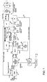
- FIG. 1 provides a system block diagram and Figure 2 illustrates the CTL loop filter steering operation during normal demodulator tracking, i.e., when no transient condition is present.
- an input signal 10 such as an RF signal received from a satellite, cable, or other communication channel is coupled to a tuner 12.
- the tuner selects one of several transmitted signals for further processing, in order to provide a service such as a video program to a user.
- the tuner frequency is maintained by an automatic frequency control (AFC) loop that comprises a prescaler output 13 and a control signal input 15.
- AFC automatic frequency control
- the prescaler output 13 is provided to a microprocessor 34, which is responsive thereto for providing the control signal input 15.
- Tuner 12 outputs an intermediate frequency (IF) signal in a conventional manner to a demodulator, such as a multiphase I/Q baseband demodulator 14.
- a demodulator such as a multiphase I/Q baseband demodulator 14.
- Multiphase demodulators are well known, for example, in order to demodulate quadrature amplitude modulated (QAM), Quadrature Phase Shift Keying (QPSK) or Offset Quadrature Phase Shift Keying (OQPSK) signals.
- QAM quadrature amplitude modulated
- QPSK Quadrature Phase Shift Keying
- OFQPSK Offset Quadrature Phase Shift Keying
- demodulator 14 is responsive to a local oscillator frequency from a voltage controlled oscillator (VCO) 16.
- VCO voltage controlled oscillator
- a prescaler 18 also receives the VCO output for providing a loop control signal to microprocessor 34.
- the microprocessor controls the VCO output frequency via a CTL VCO control voltage on line 31.
- Demodulator 14 outputs in-phase (I) and quadrature phase (Q) signal components at baseband (i.e., demodulated).
- the baseband components are input to analog-to-digital (ADC) converters, which provide corresponding I data and Q data to a carrier tracking loop phase detector and digital-to-analog converter (DAC) 26.
- ADC analog-to-digital
- DAC digital-to-analog converter
- the I and Q data is also provided to conventional forward error correction (FEC) circuitry 22.
- FEC forward error correction
- a bit timing loop 24 receives the I data as well as I-mid data from ADC's 20.
- the I-mid data represents the midpoint data of the I channel eye pattern.
- the CTL phase detector and DAC 26 determines the phase of the I and Q data inputs and converts this information to an analog signal for input to a CTL loop filter 28.
- the loop filter can comprise, for example, an operational amplifier (op amp) integrator circuit that includes an RC circuit to provide the integration.
- op amp operational amplifier
- the CTL loop filter 28 is flushed upon the occurrence of a transient signal loss in order to enable fast recovery therefrom.
- a loop flush signal is provided from microprocessor 34 upon the detection of a transient loss condition.
- the loop flush signal can, for example, be nothing more than a switched ground that grounds the capacitor of the RC integrator circuit provided in the loop filter 28.
- the loop flush zeroes the capacitor charge and directs the loop filter output voltage from the supply bias rails to a constant reference voltage at which the loop was previously locked.
- the resistance value of the RC circuit will determine the bandwidth (BW) of the loop.
- BW bandwidth
- a control voltage can be set by the microprocessor 34 via a BW control signal 29.
- the output of the CTL loop filter 28 comprises a loop filter tracking voltage that is summed in an adder 30 with a frequency sweep and CTL loop filter steering signal from a filter 38.
- Filter 38 can comprise, for example, a resistor/capacitor (RC) circuit that integrates frequency control signals input thereto.
- filter 38 receives frequency sweep signals from a frequency sweep DAC 36 that is responsive to DAC Up and DAC Down commands from the microprocessor 34.
- the DAC Up and DAC Down commands can provide fine or coarse control of the CTL VCO control voltage conditioned by the filter 38 as necessary, in response to calculations performed by the microprocessor.
- the loop filter tracking voltage from CTL loop filter 28 is also provided to an ADC 32, that converts the analog voltage from the loop filter 28 to a corresponding digital data signal which is input to microprocessor 34.
- the microprocessor determines, from the digital data, whether the magnitude of the loop filter tracking voltage is within a range ("loop flush value window") 42 defined by an upper boundary 40 and a lower boundary 44 shown in Figure 2. If the voltage is outside of the normal loop filter tracking range 42, the microprocessor will control the coarse and/or fine adjustment of the filter 38 in order to slowly drive the loop filter tracking voltage back to a point within the range 42.
- the loop filter steering is accomplished outside the CTL using a voltage tracking loop which operates at a much lower bandwidth (relative to the CTL) and operates "small signal" with respect to the CTL. This ensures that the acceleration (loop stress) effects do not cause cycle slips or bit errors in the demodulator.
- the voltage steering source is the frequency sweep DAC 36, which is also used for frequency sweeping the CTL during acquisition.
- the loop filter voltage is measured by the microprocessor 34, which compares it to the calibrated loop flush value window. If the voltage is within the window, no inputs to the frequency sweep DAC 36 are changed. If the voltage is outside the limits, then the frequency sweep DAC is adjusted (at a step size and a rate that does not exceed the CTL tracking dynamics) until the CTL tracking filter voltage is within the assigned limits.
- the transient recovery method is effective only after the CTL tracking filter voltage reaches the loop flush value (within the assigned window).
- a similar Slow DAC function is provided, and once engaged, corrections towards the calibrated target value can be made.
- a "Slow DAC" output from the microprocessor 34 via line 37 is provided to provide coarse control during CTL loop tracking. This signal is used to switch the capacitance of filter 38 in order to slow down the DAC output changes during tracking.
- the object is to steer the CTL loop filter tracking voltage 33 as fast as possible to achieve the target value so that the demodulator can be prepared to undertake the fast reacquisition procedure.
- the corrections to the DACs can be very fast, e.g., on the order of about 1.0 MHz per second acceleration into the CTL.
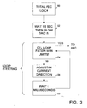
- a flowchart of the CTL loop steering process is provided in Figure 3.
- the process commences at box 50, when the FEC circuitry 22 ( Figure 1) detects total FEC lock. Then, assuming that an event such as a channel change may have just occurred, a wait (e.g., 15 seconds) is initiated as indicated at box 52 for the signals to settle out. A coarse adjustment of the filter 38 is then initiated by microprocessor 34 (via the Slow DAC function and/or via the DAC Up and DAC Down control signals), and at box 54 a determination is made as to whether the CTL loop filter output 28 is within the window 42 which represents normal loop filter tracking. If so, the AFC circuit comprising tuner prescaler 13 and control signal 15 are relied on to maintain the correct tuner frequency.
- the microprocessor 34 will initiate fine or coarse adjustment of the frequency sweep DAC 36, as necessary, in order to bring the CTL loop filter back within the normal window of operation. This step is indicated at box 56.
- a short wait (e.g., 5 milliseconds) is provided at box 58, and the CTL loop filter is again tested at box 54 to determine if it is within the proper limits of operation. This process will continue until the CTL loop filter is within the predefined window (i.e., operating with normal tracking as indicated by numeral 42 in Figure 2).
- RS Reed-Solomon
- Such a Reed-Solomon interrupt is generated by a conventional coder that uses the well known Reed-Solomon non-binary linear block code to correct symbol errors.
- a trial and error process is commenced in which the conventional Viterbi decoder contained in the digital receiver is adjusted to rotate and invert the Viterbi processing through all possible combinations of the multiphase signal constellation. This process is indicated at box 62.
- a determination is made as to whether resynchronization has been achieved. If so, there is no need to reacquire the signal and control is directed to the RS resynchronization procedure, which resynchronizes the remainder of the FEC.
- the CTL loop filter 28 is continuously flushed for a short time, such as 20 milliseconds (or for a variable time if an adaptive control is provided based on different types of transient conditions).
- the flush duration is set to accommodate the entire expected period of a transient. For example, it has been found that the duration of most transients caused by lightning strikes is less than 20 milliseconds, so a 20 ms flush period will generally be sufficient for such transients.
- the continuous loop flush or reset time is selected as a "wait for the storm to pass" time prior to enabling the CTL to reacquire.
- the loop flush time should be as short as possible, but long enough to let the transient subside. The longer the loop flush time, the more erred bits pass to the digital video pipeline which generates more visible artifacts.
- the transient recovery time can be a user programmed feature that can be optimized for the type of transient loss of carrier typically experienced at a particular site, whether it be lightning, momentary RF dropouts, momentary RF interference (such as radar), power line induced transients (that cause loss of lock without resetting the IRD), or other phenomena.
- the loop bandwidth (BW) is set by microprocessor 34 (via BW control signal 29 shown in Figure 1) to a value that will enable reacquisition.
- the loop bandwidth can be set to the previous CTL tracking bandwidth (i.e., the last bandwidth at which the CTL was properly tracking the received signal).
- a short wait (e.g., 1 millisecond) is provided at box 70 for carrier acquisition.
- a determination is made (box 72) as to whether carrier lock has been achieved. If not, the coarse and/or fine DACs are reswept by the microprocessor across an uncertainty range in an attempt to achieve carrier lock.
- resweep full frequency sweep
- Laboratory testing of the described method showed much improved performance over the previous acquisition recovery methods.
- the test consisted of inserting an interfering CW carrier (10 MHz away from the standard carrier) for a period of 5 milliseconds every 10 seconds. The interference would cause the CTL to drop lock. Recovery was successful more than 90 % of the time and the visible effects were limited to some macroblocking.
- FIG. 5 An alternate carrier reacquisition method is illustrated in Figure 5. This method is potentially faster than that shown in Figure 4, has less time for loop flush, and is generally adapted to the transient period.
- Boxes 80, 82, 84, 86, 88, 90, 92, 94 and 96 of Figure 5 correspond to boxes 60, 62, 64, 66, 68, 70, 72, 74 and 76 of Figure 4, respectively.
- the loop flush is engaged (assuming a count is below a preset value, as indicated at boxes 100, 102, 104) for a shorter time than in the Figure 4 embodiment (e.g., 1 millisecond instead of 20 milliseconds), after which the CTL loop BW is set (box 88) and allowed to acquire for 1 millisecond (box 90).
- the process repeats until carrier lock goes true or the event counter reaches the maximum predefined value.
- very short (e.g., 1 millisecond) transients are more quickly recovered from and longer (e.g., 15 millisecond) transients are also recoverable.
- the counter is reset to zero prior to the first loop flush.
- the present invention provides a method and apparatus for fast recovery from a transient loss of a received carrier in a modem, such as a satellite or terrestrial communication modem.
- the modem includes a carrier tracking loop filter, the voltage of which is steered toward a predetermined value within a "pull-in window" to minimize any change in frequency when the loop is flushed.
- the carrier tracking loop filter is flushed for a time period approximating the length of the transient.
- the carrier tracking loop is enabled, and attempts to pull in the frequency and phase of the received carrier.
Landscapes
- Digital Transmission Methods That Use Modulated Carrier Waves (AREA)
- Stabilization Of Oscillater, Synchronisation, Frequency Synthesizers (AREA)
Applications Claiming Priority (2)
| Application Number | Priority Date | Filing Date | Title |
|---|---|---|---|
| US6466697P | 1997-11-06 | 1997-11-06 | |
| US64666P | 1997-11-06 |
Publications (2)
| Publication Number | Publication Date |
|---|---|
| EP0915569A1 true EP0915569A1 (fr) | 1999-05-12 |
| EP0915569B1 EP0915569B1 (fr) | 2003-03-19 |
Family
ID=22057489
Family Applications (1)
| Application Number | Title | Priority Date | Filing Date |
|---|---|---|---|
| EP19980120698 Expired - Lifetime EP0915569B1 (fr) | 1997-11-06 | 1998-11-06 | Procédé et dispositif rapides de récupération de synchronisme dans une boucle à verrouillage de phase |
Country Status (5)
| Country | Link |
|---|---|
| EP (1) | EP0915569B1 (fr) |
| JP (1) | JPH11243335A (fr) |
| CA (1) | CA2252241A1 (fr) |
| DE (1) | DE69812272T2 (fr) |
| TW (1) | TW406484B (fr) |
Families Citing this family (1)
| Publication number | Priority date | Publication date | Assignee | Title |
|---|---|---|---|---|
| JP5793944B2 (ja) * | 2011-04-27 | 2015-10-14 | コニカミノルタ株式会社 | 誘導加熱装置及び画像形成装置 |
Citations (7)
| Publication number | Priority date | Publication date | Assignee | Title |
|---|---|---|---|---|
| US4185246A (en) * | 1978-02-27 | 1980-01-22 | Schlumberger Technology Corporation | Circuit for reducing transients by precharging capacitors |
| US4703520A (en) * | 1986-10-31 | 1987-10-27 | Motorola, Inc. | Radio transceiver having an adaptive reference oscillator |
| EP0289941A2 (fr) * | 1987-05-04 | 1988-11-09 | Motorola, Inc. | Boucle d'asservissement de phase à circuit de commande d'accrochage en fréquence rapide |
| US4855689A (en) * | 1987-02-13 | 1989-08-08 | Hughes Aircraft Company | Phase lock loop with switchable filter for acquisition and tracking modes |
| EP0402113A2 (fr) * | 1989-06-07 | 1990-12-12 | International Business Machines Corporation | Circuit de commande de fréquence pour VCO |
| EP0664616A2 (fr) * | 1994-01-21 | 1995-07-26 | AT&T Corp. | Bouche à verrouillage de phase initialisée par une valeur calibrée de contrôle de l'oscillateur |
| WO1998023036A1 (fr) * | 1996-11-21 | 1998-05-28 | Advanced Micro Devices, Inc. | Boucle de reconstitution de porteuse avec initialisation stockee dans un recepteur radio |
-
1998
- 1998-10-29 CA CA 2252241 patent/CA2252241A1/fr not_active Abandoned
- 1998-10-30 TW TW87118078A patent/TW406484B/zh not_active IP Right Cessation
- 1998-11-06 EP EP19980120698 patent/EP0915569B1/fr not_active Expired - Lifetime
- 1998-11-06 JP JP10315262A patent/JPH11243335A/ja active Pending
- 1998-11-06 DE DE1998612272 patent/DE69812272T2/de not_active Expired - Fee Related
Patent Citations (7)
| Publication number | Priority date | Publication date | Assignee | Title |
|---|---|---|---|---|
| US4185246A (en) * | 1978-02-27 | 1980-01-22 | Schlumberger Technology Corporation | Circuit for reducing transients by precharging capacitors |
| US4703520A (en) * | 1986-10-31 | 1987-10-27 | Motorola, Inc. | Radio transceiver having an adaptive reference oscillator |
| US4855689A (en) * | 1987-02-13 | 1989-08-08 | Hughes Aircraft Company | Phase lock loop with switchable filter for acquisition and tracking modes |
| EP0289941A2 (fr) * | 1987-05-04 | 1988-11-09 | Motorola, Inc. | Boucle d'asservissement de phase à circuit de commande d'accrochage en fréquence rapide |
| EP0402113A2 (fr) * | 1989-06-07 | 1990-12-12 | International Business Machines Corporation | Circuit de commande de fréquence pour VCO |
| EP0664616A2 (fr) * | 1994-01-21 | 1995-07-26 | AT&T Corp. | Bouche à verrouillage de phase initialisée par une valeur calibrée de contrôle de l'oscillateur |
| WO1998023036A1 (fr) * | 1996-11-21 | 1998-05-28 | Advanced Micro Devices, Inc. | Boucle de reconstitution de porteuse avec initialisation stockee dans un recepteur radio |
Also Published As
| Publication number | Publication date |
|---|---|
| DE69812272T2 (de) | 2004-01-29 |
| TW406484B (en) | 2000-09-21 |
| JPH11243335A (ja) | 1999-09-07 |
| CA2252241A1 (fr) | 1999-05-06 |
| EP0915569B1 (fr) | 2003-03-19 |
| DE69812272D1 (de) | 2003-04-24 |
Similar Documents
| Publication | Publication Date | Title |
|---|---|---|
| US6275554B1 (en) | Digital symbol timing recovery network | |
| CA2169551C (fr) | Dispositif et procede destines a maximiser l'execution d'une poursuite de decalage de frequence dans un recepteur numerique | |
| JP4518355B2 (ja) | Hdtv受像機の復調器のための位相誤差算定方法 | |
| CA2207288C (fr) | Circuit de commande automatique de gain et methode associee | |
| US6690740B1 (en) | Methods and apparatus for providing robust synchronization of radio transceivers | |
| EP0568646B1 (fr) | Appareil et procede de correction du decalage de courant continu dans un recepteur | |
| US6501730B1 (en) | Carrier recovery in DAB receivers | |
| US6967694B1 (en) | Demodulator for demodulating digital broadcast signals | |
| CA2003580C (fr) | Commande automatique de frequence en presence de donnees | |
| KR100686990B1 (ko) | 디지털 위성 텔레비전 수상기용의 고속의 신호 포착을달성하기 위한 동조 시스템 | |
| US5812615A (en) | Apparatus and method for maximizing frequency offset tracking performance in a digital receiver | |
| US5533059A (en) | Carrier phase lock detecting apparatus used in PSK-modulated signal receiver for satellite communication system | |
| EP1067785A2 (fr) | Oscillateur commandé dans un réseau de récupération du rythme de symboles numériques | |
| EP0915569B1 (fr) | Procédé et dispositif rapides de récupération de synchronisme dans une boucle à verrouillage de phase | |
| JP3037352B2 (ja) | サテライト無線受信機 | |
| US5815535A (en) | Carrier recovery apparatus | |
| EP0962046B1 (fr) | Systeme et procede permettant d'eviter des interferences d'harmoniques dans un circuit de reconstitution de la porteuse pour une demodulation numerique | |
| MXPA04010334A (es) | Algoritmo de busqueda de temporizacion de simbolo. | |
| CA2195926C (fr) | Demodulateur pour recepteurs de communication | |
| JP4067566B2 (ja) | Rf信号の同調された1つに対応する情報を伝える搬送波信号を生成するチューナおよびその制御方法 | |
| EP1745625B1 (fr) | Correction d'ambiguite de phase de porteuse par decalage en continu | |
| JPH0715482A (ja) | 自動周波数制御装置 | |
| KR20000044166A (ko) | 디지털 텔레비젼 수신장치의 자동이득제어회로및 방법 | |
| KR20000034320A (ko) | 디지털 통신 수신기의 심볼타이밍 복구장치 및 방법 | |
| JPH05227227A (ja) | 疑似引き込み訂正方式 |
Legal Events
| Date | Code | Title | Description |
|---|---|---|---|
| PUAI | Public reference made under article 153(3) epc to a published international application that has entered the european phase |
Free format text: ORIGINAL CODE: 0009012 |
|
| AK | Designated contracting states |
Kind code of ref document: A1 Designated state(s): DE FR GB NL |
|
| AX | Request for extension of the european patent |
Free format text: AL;LT;LV;MK;RO;SI |
|
| 17P | Request for examination filed |
Effective date: 19990929 |
|
| AKX | Designation fees paid |
Free format text: DE FR GB NL |
|
| 17Q | First examination report despatched |
Effective date: 20010302 |
|
| GRAG | Despatch of communication of intention to grant |
Free format text: ORIGINAL CODE: EPIDOS AGRA |
|
| GRAG | Despatch of communication of intention to grant |
Free format text: ORIGINAL CODE: EPIDOS AGRA |
|
| GRAH | Despatch of communication of intention to grant a patent |
Free format text: ORIGINAL CODE: EPIDOS IGRA |
|
| GRAH | Despatch of communication of intention to grant a patent |
Free format text: ORIGINAL CODE: EPIDOS IGRA |
|
| GRAA | (expected) grant |
Free format text: ORIGINAL CODE: 0009210 |
|
| AK | Designated contracting states |
Designated state(s): DE FR GB NL |
|
| PG25 | Lapsed in a contracting state [announced via postgrant information from national office to epo] |
Ref country code: NL Free format text: LAPSE BECAUSE OF FAILURE TO SUBMIT A TRANSLATION OF THE DESCRIPTION OR TO PAY THE FEE WITHIN THE PRESCRIBED TIME-LIMIT Effective date: 20030319 |
|
| REG | Reference to a national code |
Ref country code: GB Ref legal event code: FG4D |
|
| REF | Corresponds to: |
Ref document number: 69812272 Country of ref document: DE Date of ref document: 20030424 Kind code of ref document: P |
|
| NLV1 | Nl: lapsed or annulled due to failure to fulfill the requirements of art. 29p and 29m of the patents act | ||
| ET | Fr: translation filed | ||
| PLBE | No opposition filed within time limit |
Free format text: ORIGINAL CODE: 0009261 |
|
| STAA | Information on the status of an ep patent application or granted ep patent |
Free format text: STATUS: NO OPPOSITION FILED WITHIN TIME LIMIT |
|
| 26N | No opposition filed |
Effective date: 20031222 |
|
| PGFP | Annual fee paid to national office [announced via postgrant information from national office to epo] |
Ref country code: GB Payment date: 20051004 Year of fee payment: 8 |
|
| PGFP | Annual fee paid to national office [announced via postgrant information from national office to epo] |
Ref country code: FR Payment date: 20051104 Year of fee payment: 8 |
|
| PGFP | Annual fee paid to national office [announced via postgrant information from national office to epo] |
Ref country code: DE Payment date: 20051130 Year of fee payment: 8 |
|
| PG25 | Lapsed in a contracting state [announced via postgrant information from national office to epo] |
Ref country code: DE Free format text: LAPSE BECAUSE OF NON-PAYMENT OF DUE FEES Effective date: 20070601 |
|
| GBPC | Gb: european patent ceased through non-payment of renewal fee |
Effective date: 20061106 |
|
| REG | Reference to a national code |
Ref country code: FR Ref legal event code: ST Effective date: 20070731 |
|
| PG25 | Lapsed in a contracting state [announced via postgrant information from national office to epo] |
Ref country code: GB Free format text: LAPSE BECAUSE OF NON-PAYMENT OF DUE FEES Effective date: 20061106 |
|
| PG25 | Lapsed in a contracting state [announced via postgrant information from national office to epo] |
Ref country code: FR Free format text: LAPSE BECAUSE OF NON-PAYMENT OF DUE FEES Effective date: 20061130 |
|
| P01 | Opt-out of the competence of the unified patent court (upc) registered |
Effective date: 20230520 |