EP0402113A2 - Circuit de commande de fréquence pour VCO - Google Patents
Circuit de commande de fréquence pour VCO Download PDFInfo
- Publication number
- EP0402113A2 EP0402113A2 EP90306142A EP90306142A EP0402113A2 EP 0402113 A2 EP0402113 A2 EP 0402113A2 EP 90306142 A EP90306142 A EP 90306142A EP 90306142 A EP90306142 A EP 90306142A EP 0402113 A2 EP0402113 A2 EP 0402113A2
- Authority
- EP
- European Patent Office
- Prior art keywords
- frequency
- vco
- pll
- signal
- error signal
- Prior art date
- Legal status (The legal status is an assumption and is not a legal conclusion. Google has not performed a legal analysis and makes no representation as to the accuracy of the status listed.)
- Granted
Links
Images
Classifications
-
- H—ELECTRICITY
- H03—ELECTRONIC CIRCUITRY
- H03L—AUTOMATIC CONTROL, STARTING, SYNCHRONISATION OR STABILISATION OF GENERATORS OF ELECTRONIC OSCILLATIONS OR PULSES
- H03L7/00—Automatic control of frequency or phase; Synchronisation
- H03L7/06—Automatic control of frequency or phase; Synchronisation using a reference signal applied to a frequency- or phase-locked loop
- H03L7/08—Details of the phase-locked loop
- H03L7/10—Details of the phase-locked loop for assuring initial synchronisation or for broadening the capture range
- H03L7/113—Details of the phase-locked loop for assuring initial synchronisation or for broadening the capture range using frequency discriminator
-
- G—PHYSICS
- G11—INFORMATION STORAGE
- G11B—INFORMATION STORAGE BASED ON RELATIVE MOVEMENT BETWEEN RECORD CARRIER AND TRANSDUCER
- G11B20/00—Signal processing not specific to the method of recording or reproducing; Circuits therefor
- G11B20/10—Digital recording or reproducing
- G11B20/12—Formatting, e.g. arrangement of data block or words on the record carriers
- G11B20/1217—Formatting, e.g. arrangement of data block or words on the record carriers on discs
- G11B20/1258—Formatting, e.g. arrangement of data block or words on the record carriers on discs where blocks are arranged within multiple radial zones, e.g. Zone Bit Recording or Constant Density Recording discs, MCAV discs, MCLV discs
Definitions
- This invention relates to a circuit suitable for setting and dynamically adjusting the free-running frequency of a voltage controlled oscillator (VCO) in a phase-locked loop (PLL).
- VCO voltage controlled oscillator
- PLL phase-locked loop
- VCO is employed, for example, for this purpose in the design of a magnetic recording channel.
- a major problem in the design of PLLs is assuring a very tight tolerance for the free-running frequency of the VCO.
- temperature compensation technigues are often incorporated into the design of the VCO circuitry.
- the variations in process parameters are statistically independent of each other, the effect on the circuit cannot be fully overcome using design techniques.
- the VCO free-running frequency can have as much as 30%-50% variation from chip to chip.
- the free-running frequency tolerance be very tight and not vary more than 1%-2%.
- the chip-to-chip variation in VCO free-running frequency has been resolved by physically modifying the PLL chip by using (1) a laser trim technique involving trimming resistors or capacitors which are on the module substrate and connected to the VCO circuit inside the chip; or (2) a high current zapping technique to blow out resistors on the chip at the wafer level. Both of these techniques are expensive and time consuming, and the high current zapping technique is unreliable for the tight tolerances required for a VCO.
- U.S. Patent 4,380,742 describes a circuit for synchronising the frequency and/or phase of an output frequency signal to reference frequency signal.
- This phase-locked or frequency locked circuit comprises an oscillator the components of which must be trimmed, as in other prior art frequency synthesising circuits such as those described in U.S. Patents 4,654,604; 4,672,477; 3,651,422 and 4,543,661.
- the invention provides a circuit for controlling the frequency of a VCO in a PLL comprising frequency lock loop means (FLL) for initially setting the free-running frequency of the VCO to a preselected value including a first counter for counting output frequency pulses from the VCO, a second counter for counting frequency pulses from a reference clock and providing a strobe pulse on counting to a preselected count value, a register in which the then existing count in the first counter is stored in response to the strobe pulse, a comparator conditioned by the strobe pulse to compare the count stored in the register with a preselected expected count to provide an output when the stored and expected counts differ, and means responsive to the comparator output signal to provide a signal to the VCO to adjust the free-running frequency to its preselected value.
- FLL frequency lock loop means
- the circuit further includes means for maintaining the VCO frequency within a preselected frequency range comprising means responsive to the VCO output signal and a signal input to the PLL, to which the VCO signal is to be locked, to generate a signal indicative of the frequency error of the PLL, control means for summing the PLL frequency error signal and a signal representing the VCO free running frequency and supplying a control signal derived from the resultant sum to the VCO to change the VCO frequency as necessary to maintain it within the lock range.
- the VCO frequency is kept within the correction range permitted by the circuit.
- the circuit also includes means in the PLL responsive to a deviation of the VCO frequency outside the frequency range to apply a signal to means in the FLL to adjust the VCO free-running frequency to lie within the frequency range.
- means in the PLL responsive to a deviation of the VCO frequency outside the frequency range to apply a signal to means in the FLL to adjust the VCO free-running frequency to lie within the frequency range.
- Such a circuit permits the VCO frequency to be adjusted dynamically at the system level to compensate for variations in temperature, power supply, drift of components due to aging, or other factors which cause the VCO frequency to deviate from the frequency range defined within the circuit.
- the circuit should also permit the free-running frequency to be changed dynamically by programming that will adjust the frequency ratio to enable use of several different data frequencies with a single predetermined servo or other reference frequency for data banding.
- a method of controlling the frequency of a VCO in a PLL including the step of initially setting the free-running frequency of the VCO to a preselected value, comprising the steps of: (a) counting output pulses from the VCO, (b) counting pulses from a reference clock, (c) when the number of reference pulses reaches a preselected value, comparing the counted number of VCO output pulses with a preselected expected count corresponding to the preselected free-running frequency value and (d) incrementing or decrementing the VCO free-running frequency according to whether the number of counted VCO pulses is lower or higher than the expected count.
- the method further includes the step of subsequently maintaining the frequency of the VCO within a preselected frequency range, comprising the steps of: enabling the PLL; generating a phase error signal indicative of the phase and/or frequency difference between the VCO output signal and the incoming signal to the PLL, generating a frequency error signal from the phase error signal, adding the phase error and frequency error signals to generate a signal reflecting the PLL frequency error and summing the PLL frequency error signal and signal indicative of the VCO frequency to produce a voltage to adjust the VCO frequency as necessary to maintain it within the preselected frequency range.
- the method includes the step of, in response to a deviation of the VCO frequency outside the frequency range, dynamically adjusting the VCO frequency by combining the frequency error signal generated from the phase error signal with a signal indicative of the VCO frequency and summing the combination signal and PLL phase error signal to produce a voltage to restore the VCO frequency to within the frequency range.
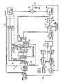
- a circuit embodying the invention which may be used to set the VCO free-running frequency in a PLL of a magnetic recording channel is shown in the figure and comprises two interconnected loops A, B (shown separated by a dotted line), an eight bit digital to analog converter (DAC) 10, a four bit DAC 11, and a VCO 12.
- DAC 10 is set to a preselected centre frequency for VCO 12, e.g. 10 MHz; and DAC 11 is set to the centre of a preselected permissible deviation or lock range (e.g., ⁇ 10 KHz) from said centre frequency.
- An analog-to-digital converter (ADC) 13, a phase error generator 14, timing control logic 15, together with the DAC 11 and VCO 12, constitute a PLL.
- Timing control logic 15 comprises an AND gate 16, an adder 17, a register 18, a multiplexor 20, and an adder 21.
- adder 17, register 18 and multiplexor 20 constitute a digital integrator 19 which converts a digital phase error signal to a digital frequency error signal.
- the PLL timing control logic 15 controls the four bit DAC 11 to adjust phase differences between the VCO output frequency and the data input frequency to ADC 13, so as normally to maintain the PLL within the preselected lock range.
- the PLL is operative to lock an output in line 22 to an analog signal supplied via an input line 23 at a desired sample phase.
- the output signal in 22 is used by the PLL and other parts (not shown) of a utilisation device, such as a magnetic recording channel.
- the circuit further comprises a FLL in combination with the PLL.
- the FLL is used to initially set the free-running frequency of VCO 12 despite variation in components due to process variations; and thereafter it is used to dynamically adjust the free-running frequency to maintain it within the preselected lock range of the PLL in the event of drift due to relatively large changes in supply voltage and/or temperature.
- the FLL comprises a line 29 for supplying servo or reference clock pulses from a source (not shown), three counters 30, 31 and 32, two comparators 33 and 34, two registers 35 and 36, a multiplexor 37, an adder 38 connected to an AND gate 39, and a summing node 40, as well as the DAC 10 and VCO 12.
- Register 36, as well as register 18, is clocked by the VCO 12 output in line 28.
- Node 40 sums the currents from the DACs 10 and 11 and their sum is converted to an analog bias voltage by resistor 29.
- the VCO output frequency is typically a ratio of two integers, N and R, whose values are dependent upon the servo architecture.
- R is the desired count of counter 31, and N is the maximum count of the reference counter 30.
- a "set free-running frequency” signal is brought up in line 41 by programming or firmware for a preselected period of time sufficient to set the free-running frequency for VCO 12.
- This signal temporarily disables the PLL in the following manner.
- the signal in 41 is applied through an inverter 42 to AND gate 16, thereby cutting off the output from phase error generator 14 and forcing the output from AND 16 to adder 21 to zero.
- the signal in 41 is applied via OR gate 43 to multiplexor 20 to connect the "0" input to adder 21. With both inputs to adder 21 zeroed, DAC 11 is set to zero in two's complement form at substantially the centre of the preselected PLL lock range.
- the signal in 41 also conditions multiplexor 37 to connect counter 32 to register 36 for activating the FLL to set the free-running frequency of VCO 12.
- the FLL is locked to the reference clock by counters 30, 31.
- the value of N is controlled by comparator 33. Each time counter 30 counts N reference clock pulses, comparator 33 issues a strobe pulse that resets counters 30, 31 and causes counter 31 to store its count of VCO pulses in register 35.
- Comparator 34 is conditioned by the strobe pulse to compare the actual count M of VCO pulses as supplied by counter 31 to register 35 in response to the previous strobe with a preset expected count R for VCO pulses. If M ⁇ R, the output of comparator 34 will increment counter 32; whereas if M > R, comparator 34 will decrement counter 32. Multiplexor 37 passes the current value of the VCO frequency from counter 32 to register 36, from which it is fed to DAC 10 and converted to a corresponding analog bias voltage. This voltage is applied via summing circuit 40 at the input to VCO 12 for causing the VCO frequency to be incremented or decremented according to whether M ⁇ R or M > R, respectively, until the contents of register 35 equals the value of R.
- the current value fed to the eight bit DAC 10 should be incremented in increments of 1, as illustrated, to progressively raise the VCO frequency by 3 units until VCO output frequency is exactly R/N times the reference clock frequency; whereupon the VCO free-running frequency is established, and the input to the eight bit DAC 10 will then be held constant. After this, four bit DAC 11 takes over to compensate for phase differences between VCO output frequency and the data input frequency to ADC 13.
- the DAC 10 preselected free-running frequency and the obtainable VCO frequency will generally not be identical, a tolerance of e.g., R ⁇ 2, would be expected. It will be apparent that by increasing the value of R, the tolerance percentage can be reduced. Also, the value of the free-running frequency can be set arbitrarily close to the desired frequency depending upon the value of R and the number of bits in DAC 10.
- phase error generator 14 After the initial setting of the VCO free-running frequency by the FLL, the frequency should normally be maintained within the required frequency range, by the PLL.
- Phase error generator 14 When the PLL disabling signal on line 41 goes down, the PLL is enabled.
- Phase error generator 14 thereafter generates a digital phase error signal indicative of the phase and/or frequency difference between the input data and the VCO output signal.
- the digital integrator 19 generates a digital frequency error signal from the phase error signal.
- the frequency and phase error signals are summed by adder 21 and the result is supplied to the DAC 11 in the PLL to provide an analog output signal indicative of the PLL frequency error.
- the outputs from DACs 10 and 11 are summed by summing circuit 40 and the resultant current is converted to a bias voltage by resistor 29 to adjust the VCO frequency as necessary for normally maintaining it within the lock range defined by DAC 11.
- phase error generator 14 If there is no frequency difference between the input signal 23 and the VCO output signal 28, then the PLL would be required to compensate solely for phase difference between the two which would be determined by phase error generator 14. Assuming for the moment that the bottom leg of adder 21 is zero (ie has no influence on the loop) then the phase error would pass through the adder via DAC 11 to VCO 12. This error would act on the VCO in such manner as to correct for this phase error. After several passes round the PLL, the phase error would be driven to zero.
- phase error caused by this frequency difference is added to the total phase error at every clock cycle.
- a second order loop This operates by adding the constant phase error, which is measured by the digital integrator 19, to the measured phase error. If at every clock cycle there is a constant phase error the digital integrator will integrate the value driving the output of the integrator toward the value of the constant phase error. The output of 19 when fed back around the loop reduces the constant phase error. When the magnitude of integrator 19 reaches a value which drives the constant phase error to zero, the integration stops because the phase error is zero.
- the FLL operates to dynamically restore the VCO free-running frequency setting to within the PLL lock range in the following manner.
- Phase error detector 14 generates a digital signal directly proportional to the amount of drift.
- AND gate 16 will pass the phase error signal to adders 21, 17 because the signal in line 41 is down.
- adder 17 overflows or underflows.
- the resultant over/underflow signal passes via OR gate 43 to multiplexor 20 which then connects its "0" input to adder 21.
- the phase error signal from AND 16 is converted to a digital frequency error signal as it passes via adder 17 and register 18 to AND 39.
- the sign bit which is of the most significant bit (MSB) in register 18 denotes whether there is an overflow or underflow condition.
- AND 39 is now enabled by the over/underflow signal and passes the contents of register 18 to adder 38.
- multiplexor 37 passes the contents of adder 38 via register 36 to DAC 10.
- the phase error signal from DAC 11 and the signal from DAC 10 are summed by summing circuit 40, and the resultant current in converted to a bias voltage to increase or decrease the VCO input frequency according to whether the frequency error indicated that the VCO frequency was too low or too high, thereby to adjust the VCO free-running frequency to within the PLL lock range.
- the ratio of the VCO frequency to the reference clock frequency can be established or modified by programming. Also different ratios and hence frequencies can be derived by suitable programming from a single servo or other reference frequency. This enables data banding, for example, in Partial Response Maximum Likelihood (PRML) and Peak Detection (PD) type magnetic recording channels.
- PRML Partial Response Maximum Likelihood
- PD Peak Detection
- This frequency is initially set by the FLL. Thereafter, the PLL is enabled and normally maintains the VCO free-running frequency within the PLL lock range. This frequency is readjusted if and when the PLL exceeds its lock range, as determined by the digital integrator 17, 18, 20. As a result, the VCO free-running frequency is maintained within the PLL lock range.
Landscapes
- Stabilization Of Oscillater, Synchronisation, Frequency Synthesizers (AREA)
- Signal Processing For Digital Recording And Reproducing (AREA)
Applications Claiming Priority (2)
| Application Number | Priority Date | Filing Date | Title |
|---|---|---|---|
| US07/363,566 US4929918A (en) | 1989-06-07 | 1989-06-07 | Setting and dynamically adjusting VCO free-running frequency at system level |
| US363566 | 1989-06-07 |
Publications (3)
| Publication Number | Publication Date |
|---|---|
| EP0402113A2 true EP0402113A2 (fr) | 1990-12-12 |
| EP0402113A3 EP0402113A3 (fr) | 1991-03-20 |
| EP0402113B1 EP0402113B1 (fr) | 1995-09-06 |
Family
ID=23430749
Family Applications (1)
| Application Number | Title | Priority Date | Filing Date |
|---|---|---|---|
| EP90306142A Expired - Lifetime EP0402113B1 (fr) | 1989-06-07 | 1990-06-06 | Circuit de commande de fréquence pour VCO |
Country Status (4)
| Country | Link |
|---|---|
| US (1) | US4929918A (fr) |
| EP (1) | EP0402113B1 (fr) |
| JP (1) | JPH0329516A (fr) |
| DE (1) | DE69022122T2 (fr) |
Cited By (14)
| Publication number | Priority date | Publication date | Assignee | Title |
|---|---|---|---|---|
| EP0540119A3 (en) * | 1991-10-30 | 1993-12-08 | Ibm | Monolithic digital phaselock loop circuit |
| DE4228834A1 (de) * | 1992-08-29 | 1994-03-03 | Thomson Brandt Gmbh | Verfahren und Vorrichtung zum Abgleich einer PLL Stufe |
| EP0557856A3 (fr) * | 1992-02-25 | 1994-04-27 | Thomson Consumer Electronics | |
| WO1995031861A1 (fr) * | 1994-05-12 | 1995-11-23 | Thomas Atkin Denning Riley | Synthetiseur fractionnaire de frequences n a discriminateur de frequences delta-sigma |
| WO1997023048A1 (fr) * | 1995-12-20 | 1997-06-26 | Robert Bosch Gmbh | Procede de synchronisation d'impulsions d'horloge |
| EP0795234A4 (fr) * | 1994-11-28 | 1998-01-21 | Univ Curtin Tech | Boucle a phase asservie a frequence pilotee |
| WO1998039847A1 (fr) * | 1997-03-04 | 1998-09-11 | Level One Communications, Inc. | Comportement d'une boucle asservie en phase a bande etroite a effet d'emulation sur une boucle asservie en phase a bande large |
| EP0866559A1 (fr) * | 1997-03-20 | 1998-09-23 | Nortel Networks Corporation | Boucle à verrouillage de phase |
| US5901119A (en) * | 1996-08-23 | 1999-05-04 | Sony Corporation | Recording apparatus, playback apparatus and recording medium having a management area with program position and playback information |
| EP0915569A1 (fr) * | 1997-11-06 | 1999-05-12 | General Instrument Corporation | Procédé et dispositif rapides de récupération de synchronisme dans une boucle à verrouillage de phase |
| EP1039640A1 (fr) * | 1999-03-26 | 2000-09-27 | Sanyo Electric Co., Ltd. | Circuit à boucle de verrouillage de phase |
| EP1050965A3 (fr) * | 1999-05-03 | 2002-03-06 | STMicroelectronics GmbH | Circuit électrique de commande d'une charge |
| WO2004059847A1 (fr) * | 2002-12-23 | 2004-07-15 | Infineon Technologies Ag | Oscillateur a commande numerique |
| WO2004079912A1 (fr) * | 2003-03-04 | 2004-09-16 | Tait Electronics Limited | Ameliorations de frequence et/ou de boucles a phase asservie |
Families Citing this family (33)
| Publication number | Priority date | Publication date | Assignee | Title |
|---|---|---|---|---|
| US5220466A (en) * | 1991-05-21 | 1993-06-15 | International Business Machines Corporation | Method and apparatus for digital filter control in a partial-response maximum-likelihood disk drive system |
| JP2648554B2 (ja) * | 1992-08-13 | 1997-09-03 | インターナショナル・ビジネス・マシーンズ・コーポレイション | Prmlディスク駆動システムの非同期ゲイン調整方法および装置 |
| US5302916A (en) * | 1992-12-21 | 1994-04-12 | At&T Bell Laboratories | Wide range digital frequency detector |
| US5424881A (en) | 1993-02-01 | 1995-06-13 | Cirrus Logic, Inc. | Synchronous read channel |
| AU6637594A (en) * | 1993-04-20 | 1994-11-08 | Rca Thomson Licensing Corporation | A phase lock loop with error consistency detector |
| US5614870A (en) * | 1993-04-20 | 1997-03-25 | Rca Thomson Licensing Corporation | Phase lock loop with idle mode of operation during vertical blanking |
| US5406592A (en) * | 1993-07-30 | 1995-04-11 | At&T Corp. | First order FLL/PLL system with low phase error |
| US5576666A (en) * | 1993-11-12 | 1996-11-19 | Nippondenso Technical Center Usa, Inc. | Fractional-N frequency synthesizer with temperature compensation |
| US5835544A (en) * | 1993-12-24 | 1998-11-10 | Sony Corporation | Clock signal reproduction circuit and data reproduction circuit |
| US5568512A (en) * | 1994-07-27 | 1996-10-22 | Micron Communications, Inc. | Communication system having transmitter frequency control |
| US5787134A (en) * | 1994-09-12 | 1998-07-28 | Analog Devices, Inc. | Switched capacitance phase locked loop system |
| US5414390A (en) * | 1994-09-12 | 1995-05-09 | Analog Devices, Inc. | Center frequency controlled phase locked loop system |
| US5635934A (en) * | 1995-03-07 | 1997-06-03 | National Semiconductor Corporation | Digital read channel utilizing analog-to-digital converter with offset reduction |
| US5546433A (en) * | 1995-03-21 | 1996-08-13 | National Semiconductor Corporation | Digital phase lock loop having frequency offset cancellation circuitry |
| US5604465A (en) * | 1995-06-07 | 1997-02-18 | International Business Machines Corporation | Adaptive self-calibration for fast tuning phaselock loops |
| US5552750A (en) * | 1995-09-05 | 1996-09-03 | Motorola, Inc. | Method and apparatus for determining an instantaneous phase difference between two signals |
| DE19601013A1 (de) * | 1996-01-13 | 1997-07-17 | Bosch Gmbh Robert | Verfahren und Anordnung zur Frequenzmodulation eines hochfrequenten Signals |
| JP2914287B2 (ja) * | 1996-03-08 | 1999-06-28 | 日本電気株式会社 | Pll回路 |
| US6362737B1 (en) * | 1998-06-02 | 2002-03-26 | Rf Code, Inc. | Object Identification system with adaptive transceivers and methods of operation |
| US5736904A (en) * | 1996-12-02 | 1998-04-07 | Motorola, Inc. | Automatic trimming of a controlled oscillator in a phase locked loop |
| KR100209739B1 (ko) * | 1997-04-28 | 1999-07-15 | 구본준 | 주파수 발생장치 |
| DE19959265A1 (de) * | 1999-12-03 | 2001-06-07 | Deutsche Telephonwerk Kabel | Verfahren zum Regeln der von einem frequenzsteuerbaren Oszillator abgegebenen Ausgangsfrequenz |
| US6920516B2 (en) * | 2000-08-31 | 2005-07-19 | Hewlett-Packard Development Company, L.P. | Anti-starvation interrupt protocol |
| US6281727B1 (en) | 2000-10-05 | 2001-08-28 | Pericom Semiconductor Corp. | Fine-tuning phase-locked loop PLL using variable resistor between dual PLL loops |
| JP4213359B2 (ja) * | 2001-05-11 | 2009-01-21 | 富士通マイクロエレクトロニクス株式会社 | 信号生成回路、タイミングリカバリpll,信号生成システム及び信号生成方法 |
| US6720834B2 (en) | 2002-04-11 | 2004-04-13 | Skyworks Solutions, Inc. | Tunable resonant circuit and voltage controlled oscillator using same |
| US6734748B2 (en) * | 2002-07-29 | 2004-05-11 | International Business Machines Corporation | Phase-locked loop oscillator with counter bypass |
| US6914489B2 (en) | 2002-09-26 | 2005-07-05 | Koninklijke Philips Electronics N.V. | Voltage-controlled oscillator presetting circuit |
| US6778024B2 (en) * | 2002-11-14 | 2004-08-17 | Gennum Corporation | Dynamically trimmed voltage controlled oscillator |
| US6788229B1 (en) * | 2003-03-14 | 2004-09-07 | Intersil Americas Inc. | Margining pin interface circuit for clock adjustment of digital to analog converter |
| US7171576B2 (en) * | 2003-04-09 | 2007-01-30 | International Business Machines Corporation | Method, apparatus and program storage device for providing clocks to multiple frequency domains using a single input clock of variable frequency |
| US6762634B1 (en) | 2003-08-13 | 2004-07-13 | Pericom Semiconductor Corp. | Dual-loop PLL with DAC offset for frequency shift while maintaining input tracking |
| CN113055112A (zh) * | 2021-03-15 | 2021-06-29 | 陕西天基通信科技有限责任公司 | 一种无线中继直放站自激检测方法、系统、设备及储存介质 |
Family Cites Families (13)
| Publication number | Priority date | Publication date | Assignee | Title |
|---|---|---|---|---|
| GB1264903A (fr) * | 1969-07-31 | 1972-02-23 | ||
| US3710274A (en) * | 1971-04-12 | 1973-01-09 | Logimetrics Inc | Frequency control of oscillators using digital techniques |
| JPS4979151A (fr) * | 1972-12-01 | 1974-07-31 | ||
| DE2856320A1 (de) * | 1978-12-27 | 1980-07-17 | Roehm Gmbh | Enzymatisches beizverfahren |
| JPS5676636A (en) * | 1979-11-29 | 1981-06-24 | Sony Corp | Variable oscillation circuit |
| US4380742A (en) * | 1980-08-04 | 1983-04-19 | Texas Instruments Incorporated | Frequency/phase locked loop circuit using digitally controlled oscillator |
| DE3126116A1 (de) * | 1981-07-02 | 1983-01-20 | Blaupunkt-Werke Gmbh, 3200 Hildesheim | Abstimmeinrichtung fuer digitale senderwahl in rundfunkempfaengern, insbesondere in ukw-empfaengern |
| FR2513458A1 (fr) * | 1981-09-23 | 1983-03-25 | Trt Telecom Radio Electr | Procede de gestion des commandes de frequence d'un poste emetteur-recepteur et de la programmation du compteur programmable de son synthetiseur numerique de frequence |
| US4528523A (en) * | 1982-12-20 | 1985-07-09 | Rca Corporation | Fast tuned phase locked loop frequency control system |
| GB8414449D0 (en) * | 1984-06-06 | 1984-07-11 | Motorola Inc | Voltage controlled oscillator |
| DE3432313A1 (de) * | 1984-09-03 | 1986-03-13 | Philips Patentverwaltung Gmbh, 2000 Hamburg | Schaltungsanordnung zum synchronisieren eines signals |
| US4633298A (en) * | 1984-11-30 | 1986-12-30 | Rca Corporation | Digitally controlled phase locked loop system having coarse and fine locking modes |
| JPS62296623A (ja) * | 1986-06-16 | 1987-12-23 | Nec Corp | 位相同期回路 |
-
1989
- 1989-06-07 US US07/363,566 patent/US4929918A/en not_active Expired - Fee Related
-
1990
- 1990-06-06 DE DE69022122T patent/DE69022122T2/de not_active Expired - Fee Related
- 1990-06-06 EP EP90306142A patent/EP0402113B1/fr not_active Expired - Lifetime
- 1990-06-06 JP JP2146413A patent/JPH0329516A/ja active Pending
Cited By (22)
| Publication number | Priority date | Publication date | Assignee | Title |
|---|---|---|---|---|
| EP0540119A3 (en) * | 1991-10-30 | 1993-12-08 | Ibm | Monolithic digital phaselock loop circuit |
| EP0557856A3 (fr) * | 1992-02-25 | 1994-04-27 | Thomson Consumer Electronics | |
| TR28311A (tr) * | 1992-02-25 | 1996-04-09 | Thomson Consumer Electronics | Bir adaptif faza kilitli döngü. |
| DE4228834A1 (de) * | 1992-08-29 | 1994-03-03 | Thomson Brandt Gmbh | Verfahren und Vorrichtung zum Abgleich einer PLL Stufe |
| WO1995031861A1 (fr) * | 1994-05-12 | 1995-11-23 | Thomas Atkin Denning Riley | Synthetiseur fractionnaire de frequences n a discriminateur de frequences delta-sigma |
| US5781044A (en) * | 1994-05-12 | 1998-07-14 | Northern Telecom Limited | Delta-sigma fractional-N frequency synthesizer and frequency discriminator suitable for use therein |
| EP0795234A4 (fr) * | 1994-11-28 | 1998-01-21 | Univ Curtin Tech | Boucle a phase asservie a frequence pilotee |
| US6031428A (en) * | 1994-11-28 | 2000-02-29 | Curtin University Of Technology | Steered frequency phase locked loop |
| WO1997023048A1 (fr) * | 1995-12-20 | 1997-06-26 | Robert Bosch Gmbh | Procede de synchronisation d'impulsions d'horloge |
| US5901119A (en) * | 1996-08-23 | 1999-05-04 | Sony Corporation | Recording apparatus, playback apparatus and recording medium having a management area with program position and playback information |
| WO1998039847A1 (fr) * | 1997-03-04 | 1998-09-11 | Level One Communications, Inc. | Comportement d'une boucle asservie en phase a bande etroite a effet d'emulation sur une boucle asservie en phase a bande large |
| EP0866559A1 (fr) * | 1997-03-20 | 1998-09-23 | Nortel Networks Corporation | Boucle à verrouillage de phase |
| KR100545947B1 (ko) * | 1997-03-20 | 2006-03-23 | 노오텔 네트웍스 리미티드 | 위상고정루프 |
| EP0915569A1 (fr) * | 1997-11-06 | 1999-05-12 | General Instrument Corporation | Procédé et dispositif rapides de récupération de synchronisme dans une boucle à verrouillage de phase |
| EP1039640A1 (fr) * | 1999-03-26 | 2000-09-27 | Sanyo Electric Co., Ltd. | Circuit à boucle de verrouillage de phase |
| US6351164B1 (en) | 1999-03-26 | 2002-02-26 | Sanyo Electric Co., Ltd. | PLL circuit |
| KR100438631B1 (ko) * | 1999-03-26 | 2004-07-03 | 산요덴키가부시키가이샤 | Pll 회로 |
| EP1050965A3 (fr) * | 1999-05-03 | 2002-03-06 | STMicroelectronics GmbH | Circuit électrique de commande d'une charge |
| WO2004059847A1 (fr) * | 2002-12-23 | 2004-07-15 | Infineon Technologies Ag | Oscillateur a commande numerique |
| US7081583B2 (en) | 2002-12-23 | 2006-07-25 | Infineon Technologies Ag | Digitally controllable oscillator |
| WO2004079912A1 (fr) * | 2003-03-04 | 2004-09-16 | Tait Electronics Limited | Ameliorations de frequence et/ou de boucles a phase asservie |
| US7411461B2 (en) | 2003-03-04 | 2008-08-12 | Tait Electronics Limited | Frequency and/or phase lock loops with beat frequency estimation |
Also Published As
| Publication number | Publication date |
|---|---|
| DE69022122T2 (de) | 1996-05-02 |
| DE69022122D1 (de) | 1995-10-12 |
| US4929918A (en) | 1990-05-29 |
| EP0402113A3 (fr) | 1991-03-20 |
| JPH0329516A (ja) | 1991-02-07 |
| EP0402113B1 (fr) | 1995-09-06 |
Similar Documents
| Publication | Publication Date | Title |
|---|---|---|
| EP0402113B1 (fr) | Circuit de commande de fréquence pour VCO | |
| US3882412A (en) | Drift compensated phase lock loop | |
| US5563552A (en) | System and method for calibrating damping factor of analog PLL | |
| US5646564A (en) | Phase-locked delay loop for clock correction | |
| US7177611B2 (en) | Hybrid control of phase locked loops | |
| US5168245A (en) | Monolithic digital phaselock loop circuit having an expanded pull-in range | |
| EP0316543B1 (fr) | Synthétiseur de fréquence ayant un détecteur numérique de phase à commande optimale et indicateur de verrouillage du type à niveau | |
| US6667663B2 (en) | Phase locked loop circuit | |
| US4980899A (en) | Method and apparatus for synchronization of a clock signal generator particularly useful in a digital telecommunications exchange | |
| CA1236534A (fr) | Circuit de centrage a oscillateur commande par tension | |
| WO1980000901A1 (fr) | Methode et dispositif de reglage de la position de phase d'un signal commande par rapport a un signal de reference dans un systeme de telecommunications | |
| US11152947B2 (en) | Feedback control for accurate signal generation | |
| US6229400B1 (en) | Method and apparatus for a calibrated frequency modulation phase locked loop | |
| US4048581A (en) | Oscillator frequency control loop | |
| US6160861A (en) | Method and apparatus for a frequency modulation phase locked loop | |
| JPS63200618A (ja) | 位相同期ループ回路 | |
| US6757349B1 (en) | PLL frequency synthesizer with lock detection circuit | |
| EP0571148B1 (fr) | Circuit de commande automatique de gain non-linéaire pour utilisation dans une boucle à verrouillage de phase | |
| US4970474A (en) | Analog/digital phase locked loop | |
| AU568189B2 (en) | Precision control frequency synthesizer having an unstable, variable frequency input signal | |
| EP0697151B1 (fr) | Oscillator a commande numerique et boucle a phase bloquee numerique asservie | |
| US6512470B2 (en) | Method of voltage controlled oscillator digital/analog converted value adjustment of compact disk read only memory device | |
| US7308066B2 (en) | Clock recovery circuit capable of automatically adjusting frequency range of VCO | |
| JP3505263B2 (ja) | Pllシンセサイザ | |
| US20030003888A1 (en) | Arrangement for generating a decoder clock signal |
Legal Events
| Date | Code | Title | Description |
|---|---|---|---|
| PUAI | Public reference made under article 153(3) epc to a published international application that has entered the european phase |
Free format text: ORIGINAL CODE: 0009012 |
|
| AK | Designated contracting states |
Kind code of ref document: A2 Designated state(s): DE FR GB |
|
| PUAL | Search report despatched |
Free format text: ORIGINAL CODE: 0009013 |
|
| 17P | Request for examination filed |
Effective date: 19901213 |
|
| AK | Designated contracting states |
Kind code of ref document: A3 Designated state(s): DE FR GB |
|
| 17Q | First examination report despatched |
Effective date: 19930901 |
|
| GRAA | (expected) grant |
Free format text: ORIGINAL CODE: 0009210 |
|
| AK | Designated contracting states |
Kind code of ref document: B1 Designated state(s): DE FR GB |
|
| REF | Corresponds to: |
Ref document number: 69022122 Country of ref document: DE Date of ref document: 19951012 |
|
| ET | Fr: translation filed | ||
| PG25 | Lapsed in a contracting state [announced via postgrant information from national office to epo] |
Ref country code: GB Effective date: 19960606 |
|
| PLBE | No opposition filed within time limit |
Free format text: ORIGINAL CODE: 0009261 |
|
| STAA | Information on the status of an ep patent application or granted ep patent |
Free format text: STATUS: NO OPPOSITION FILED WITHIN TIME LIMIT |
|
| 26N | No opposition filed | ||
| GBPC | Gb: european patent ceased through non-payment of renewal fee |
Effective date: 19960606 |
|
| PG25 | Lapsed in a contracting state [announced via postgrant information from national office to epo] |
Ref country code: FR Effective date: 19970228 |
|
| PG25 | Lapsed in a contracting state [announced via postgrant information from national office to epo] |
Ref country code: DE Effective date: 19970301 |
|
| REG | Reference to a national code |
Ref country code: FR Ref legal event code: ST |