EP0917191A2 - Elektronische Bauelementeinheit, elektronischer Zusammenbau welcher diese Einheit anwendet, und Herstellungsverfahren für diese elektronische Bauelementeinheit - Google Patents
Elektronische Bauelementeinheit, elektronischer Zusammenbau welcher diese Einheit anwendet, und Herstellungsverfahren für diese elektronische Bauelementeinheit Download PDFInfo
- Publication number
- EP0917191A2 EP0917191A2 EP98121864A EP98121864A EP0917191A2 EP 0917191 A2 EP0917191 A2 EP 0917191A2 EP 98121864 A EP98121864 A EP 98121864A EP 98121864 A EP98121864 A EP 98121864A EP 0917191 A2 EP0917191 A2 EP 0917191A2
- Authority
- EP
- European Patent Office
- Prior art keywords
- electronic component
- substrate
- component unit
- manufacturing
- roughened
- Prior art date
- Legal status (The legal status is an assumption and is not a legal conclusion. Google has not performed a legal analysis and makes no representation as to the accuracy of the status listed.)
- Withdrawn
Links
Images




Classifications
-
- H—ELECTRICITY
- H05—ELECTRIC TECHNIQUES NOT OTHERWISE PROVIDED FOR
- H05K—PRINTED CIRCUITS; CASINGS OR CONSTRUCTIONAL DETAILS OF ELECTRIC APPARATUS; MANUFACTURE OF ASSEMBLAGES OF ELECTRICAL COMPONENTS
- H05K1/00—Printed circuits
- H05K1/02—Details
- H05K1/11—Printed elements for providing electric connections to or between printed circuits
- H05K1/111—Pads for surface mounting, e.g. lay-out
-
- H—ELECTRICITY
- H05—ELECTRIC TECHNIQUES NOT OTHERWISE PROVIDED FOR
- H05K—PRINTED CIRCUITS; CASINGS OR CONSTRUCTIONAL DETAILS OF ELECTRIC APPARATUS; MANUFACTURE OF ASSEMBLAGES OF ELECTRICAL COMPONENTS
- H05K3/00—Apparatus or processes for manufacturing printed circuits
- H05K3/30—Assembling printed circuits with electric components, e.g. with resistors
- H05K3/32—Assembling printed circuits with electric components, e.g. with resistors electrically connecting electric components or wires to printed circuits
- H05K3/321—Assembling printed circuits with electric components, e.g. with resistors electrically connecting electric components or wires to printed circuits by conductive adhesives
-
- H—ELECTRICITY
- H10—SEMICONDUCTOR DEVICES; ELECTRIC SOLID-STATE DEVICES NOT OTHERWISE PROVIDED FOR
- H10W—GENERIC PACKAGES, INTERCONNECTIONS, CONNECTORS OR OTHER CONSTRUCTIONAL DETAILS OF DEVICES COVERED BY CLASS H10
- H10W70/00—Package substrates; Interposers; Redistribution layers [RDL]
- H10W70/60—Insulating or insulated package substrates; Interposers; Redistribution layers
-
- H—ELECTRICITY
- H10—SEMICONDUCTOR DEVICES; ELECTRIC SOLID-STATE DEVICES NOT OTHERWISE PROVIDED FOR
- H10W—GENERIC PACKAGES, INTERCONNECTIONS, CONNECTORS OR OTHER CONSTRUCTIONAL DETAILS OF DEVICES COVERED BY CLASS H10
- H10W74/00—Encapsulations, e.g. protective coatings
- H10W74/01—Manufacture or treatment
- H10W74/012—Manufacture or treatment of encapsulations on active surfaces of flip-chip devices, e.g. forming underfills
-
- H—ELECTRICITY
- H10—SEMICONDUCTOR DEVICES; ELECTRIC SOLID-STATE DEVICES NOT OTHERWISE PROVIDED FOR
- H10W—GENERIC PACKAGES, INTERCONNECTIONS, CONNECTORS OR OTHER CONSTRUCTIONAL DETAILS OF DEVICES COVERED BY CLASS H10
- H10W74/00—Encapsulations, e.g. protective coatings
- H10W74/10—Encapsulations, e.g. protective coatings characterised by their shape or disposition
- H10W74/15—Encapsulations, e.g. protective coatings characterised by their shape or disposition on active surfaces of flip-chip devices, e.g. underfills
-
- H—ELECTRICITY
- H05—ELECTRIC TECHNIQUES NOT OTHERWISE PROVIDED FOR
- H05K—PRINTED CIRCUITS; CASINGS OR CONSTRUCTIONAL DETAILS OF ELECTRIC APPARATUS; MANUFACTURE OF ASSEMBLAGES OF ELECTRICAL COMPONENTS
- H05K1/00—Printed circuits
- H05K1/02—Details
- H05K1/03—Use of materials for the substrate
- H05K1/0306—Inorganic insulating substrates, e.g. ceramic, glass
-
- H—ELECTRICITY
- H05—ELECTRIC TECHNIQUES NOT OTHERWISE PROVIDED FOR
- H05K—PRINTED CIRCUITS; CASINGS OR CONSTRUCTIONAL DETAILS OF ELECTRIC APPARATUS; MANUFACTURE OF ASSEMBLAGES OF ELECTRICAL COMPONENTS
- H05K1/00—Printed circuits
- H05K1/02—Details
- H05K1/09—Use of materials for the conductive, e.g. metallic pattern
- H05K1/092—Dispersed materials, e.g. conductive pastes or inks
-
- H—ELECTRICITY
- H05—ELECTRIC TECHNIQUES NOT OTHERWISE PROVIDED FOR
- H05K—PRINTED CIRCUITS; CASINGS OR CONSTRUCTIONAL DETAILS OF ELECTRIC APPARATUS; MANUFACTURE OF ASSEMBLAGES OF ELECTRICAL COMPONENTS
- H05K2201/00—Indexing scheme relating to printed circuits covered by H05K1/00
- H05K2201/01—Dielectrics
- H05K2201/0137—Materials
- H05K2201/017—Glass ceramic coating, e.g. formed on inorganic substrate
-
- H—ELECTRICITY
- H05—ELECTRIC TECHNIQUES NOT OTHERWISE PROVIDED FOR
- H05K—PRINTED CIRCUITS; CASINGS OR CONSTRUCTIONAL DETAILS OF ELECTRIC APPARATUS; MANUFACTURE OF ASSEMBLAGES OF ELECTRICAL COMPONENTS
- H05K2201/00—Indexing scheme relating to printed circuits covered by H05K1/00
- H05K2201/03—Conductive materials
- H05K2201/0332—Structure of the conductor
- H05K2201/0364—Conductor shape
- H05K2201/0367—Metallic bump or raised conductor not used as solder bump
-
- H—ELECTRICITY
- H05—ELECTRIC TECHNIQUES NOT OTHERWISE PROVIDED FOR
- H05K—PRINTED CIRCUITS; CASINGS OR CONSTRUCTIONAL DETAILS OF ELECTRIC APPARATUS; MANUFACTURE OF ASSEMBLAGES OF ELECTRICAL COMPONENTS
- H05K2201/00—Indexing scheme relating to printed circuits covered by H05K1/00
- H05K2201/03—Conductive materials
- H05K2201/0332—Structure of the conductor
- H05K2201/0364—Conductor shape
- H05K2201/0373—Conductors having a fine structure, e.g. providing a plurality of contact points with a structured tool
-
- H—ELECTRICITY
- H05—ELECTRIC TECHNIQUES NOT OTHERWISE PROVIDED FOR
- H05K—PRINTED CIRCUITS; CASINGS OR CONSTRUCTIONAL DETAILS OF ELECTRIC APPARATUS; MANUFACTURE OF ASSEMBLAGES OF ELECTRICAL COMPONENTS
- H05K2201/00—Indexing scheme relating to printed circuits covered by H05K1/00
- H05K2201/10—Details of components or other objects attached to or integrated in a printed circuit board
- H05K2201/10613—Details of electrical connections of non-printed components, e.g. special leads
- H05K2201/10621—Components characterised by their electrical contacts
- H05K2201/10674—Flip chip
-
- H—ELECTRICITY
- H05—ELECTRIC TECHNIQUES NOT OTHERWISE PROVIDED FOR
- H05K—PRINTED CIRCUITS; CASINGS OR CONSTRUCTIONAL DETAILS OF ELECTRIC APPARATUS; MANUFACTURE OF ASSEMBLAGES OF ELECTRICAL COMPONENTS
- H05K2201/00—Indexing scheme relating to printed circuits covered by H05K1/00
- H05K2201/10—Details of components or other objects attached to or integrated in a printed circuit board
- H05K2201/10613—Details of electrical connections of non-printed components, e.g. special leads
- H05K2201/10954—Other details of electrical connections
- H05K2201/10977—Encapsulated connections
-
- H—ELECTRICITY
- H05—ELECTRIC TECHNIQUES NOT OTHERWISE PROVIDED FOR
- H05K—PRINTED CIRCUITS; CASINGS OR CONSTRUCTIONAL DETAILS OF ELECTRIC APPARATUS; MANUFACTURE OF ASSEMBLAGES OF ELECTRICAL COMPONENTS
- H05K2203/00—Indexing scheme relating to apparatus or processes for manufacturing printed circuits covered by H05K3/00
- H05K2203/02—Details related to mechanical or acoustic processing, e.g. drilling, punching, cutting, using ultrasound
- H05K2203/025—Abrading, e.g. grinding or sand blasting
-
- H—ELECTRICITY
- H05—ELECTRIC TECHNIQUES NOT OTHERWISE PROVIDED FOR
- H05K—PRINTED CIRCUITS; CASINGS OR CONSTRUCTIONAL DETAILS OF ELECTRIC APPARATUS; MANUFACTURE OF ASSEMBLAGES OF ELECTRICAL COMPONENTS
- H05K2203/00—Indexing scheme relating to apparatus or processes for manufacturing printed circuits covered by H05K3/00
- H05K2203/02—Details related to mechanical or acoustic processing, e.g. drilling, punching, cutting, using ultrasound
- H05K2203/0285—Using ultrasound, e.g. for cleaning, soldering or wet treatment
-
- H—ELECTRICITY
- H05—ELECTRIC TECHNIQUES NOT OTHERWISE PROVIDED FOR
- H05K—PRINTED CIRCUITS; CASINGS OR CONSTRUCTIONAL DETAILS OF ELECTRIC APPARATUS; MANUFACTURE OF ASSEMBLAGES OF ELECTRICAL COMPONENTS
- H05K2203/00—Indexing scheme relating to apparatus or processes for manufacturing printed circuits covered by H05K3/00
- H05K2203/03—Metal processing
- H05K2203/0307—Providing micro- or nanometer scale roughness on a metal surface, e.g. by plating of nodules or dendrites
-
- H—ELECTRICITY
- H05—ELECTRIC TECHNIQUES NOT OTHERWISE PROVIDED FOR
- H05K—PRINTED CIRCUITS; CASINGS OR CONSTRUCTIONAL DETAILS OF ELECTRIC APPARATUS; MANUFACTURE OF ASSEMBLAGES OF ELECTRICAL COMPONENTS
- H05K2203/00—Indexing scheme relating to apparatus or processes for manufacturing printed circuits covered by H05K3/00
- H05K2203/09—Treatments involving charged particles
- H05K2203/095—Plasma, e.g. for treating a substrate to improve adhesion with a conductor or for cleaning holes
-
- H—ELECTRICITY
- H05—ELECTRIC TECHNIQUES NOT OTHERWISE PROVIDED FOR
- H05K—PRINTED CIRCUITS; CASINGS OR CONSTRUCTIONAL DETAILS OF ELECTRIC APPARATUS; MANUFACTURE OF ASSEMBLAGES OF ELECTRICAL COMPONENTS
- H05K3/00—Apparatus or processes for manufacturing printed circuits
- H05K3/22—Secondary treatment of printed circuits
- H05K3/28—Applying non-metallic protective coatings
-
- H—ELECTRICITY
- H05—ELECTRIC TECHNIQUES NOT OTHERWISE PROVIDED FOR
- H05K—PRINTED CIRCUITS; CASINGS OR CONSTRUCTIONAL DETAILS OF ELECTRIC APPARATUS; MANUFACTURE OF ASSEMBLAGES OF ELECTRICAL COMPONENTS
- H05K3/00—Apparatus or processes for manufacturing printed circuits
- H05K3/38—Improvement of the adhesion between the insulating substrate and the metal
- H05K3/382—Improvement of the adhesion between the insulating substrate and the metal by special treatment of the metal
-
- H—ELECTRICITY
- H10—SEMICONDUCTOR DEVICES; ELECTRIC SOLID-STATE DEVICES NOT OTHERWISE PROVIDED FOR
- H10W—GENERIC PACKAGES, INTERCONNECTIONS, CONNECTORS OR OTHER CONSTRUCTIONAL DETAILS OF DEVICES COVERED BY CLASS H10
- H10W72/00—Interconnections or connectors in packages
- H10W72/01—Manufacture or treatment
- H10W72/012—Manufacture or treatment of bump connectors, dummy bumps or thermal bumps
- H10W72/01221—Manufacture or treatment of bump connectors, dummy bumps or thermal bumps using local deposition
- H10W72/01225—Manufacture or treatment of bump connectors, dummy bumps or thermal bumps using local deposition in solid form, e.g. by using a powder or by stud bumping
-
- H—ELECTRICITY
- H10—SEMICONDUCTOR DEVICES; ELECTRIC SOLID-STATE DEVICES NOT OTHERWISE PROVIDED FOR
- H10W—GENERIC PACKAGES, INTERCONNECTIONS, CONNECTORS OR OTHER CONSTRUCTIONAL DETAILS OF DEVICES COVERED BY CLASS H10
- H10W72/00—Interconnections or connectors in packages
- H10W72/071—Connecting or disconnecting
- H10W72/072—Connecting or disconnecting of bump connectors
- H10W72/07231—Techniques
- H10W72/07236—Soldering or alloying
-
- H—ELECTRICITY
- H10—SEMICONDUCTOR DEVICES; ELECTRIC SOLID-STATE DEVICES NOT OTHERWISE PROVIDED FOR
- H10W—GENERIC PACKAGES, INTERCONNECTIONS, CONNECTORS OR OTHER CONSTRUCTIONAL DETAILS OF DEVICES COVERED BY CLASS H10
- H10W72/00—Interconnections or connectors in packages
- H10W72/071—Connecting or disconnecting
- H10W72/073—Connecting or disconnecting of die-attach connectors
-
- H—ELECTRICITY
- H10—SEMICONDUCTOR DEVICES; ELECTRIC SOLID-STATE DEVICES NOT OTHERWISE PROVIDED FOR
- H10W—GENERIC PACKAGES, INTERCONNECTIONS, CONNECTORS OR OTHER CONSTRUCTIONAL DETAILS OF DEVICES COVERED BY CLASS H10
- H10W72/00—Interconnections or connectors in packages
- H10W72/071—Connecting or disconnecting
- H10W72/073—Connecting or disconnecting of die-attach connectors
- H10W72/07331—Connecting techniques
-
- H—ELECTRICITY
- H10—SEMICONDUCTOR DEVICES; ELECTRIC SOLID-STATE DEVICES NOT OTHERWISE PROVIDED FOR
- H10W—GENERIC PACKAGES, INTERCONNECTIONS, CONNECTORS OR OTHER CONSTRUCTIONAL DETAILS OF DEVICES COVERED BY CLASS H10
- H10W72/00—Interconnections or connectors in packages
- H10W72/20—Bump connectors, e.g. solder bumps or copper pillars; Dummy bumps; Thermal bumps
- H10W72/251—Materials
-
- H—ELECTRICITY
- H10—SEMICONDUCTOR DEVICES; ELECTRIC SOLID-STATE DEVICES NOT OTHERWISE PROVIDED FOR
- H10W—GENERIC PACKAGES, INTERCONNECTIONS, CONNECTORS OR OTHER CONSTRUCTIONAL DETAILS OF DEVICES COVERED BY CLASS H10
- H10W72/00—Interconnections or connectors in packages
- H10W72/30—Die-attach connectors
- H10W72/321—Structures or relative sizes of die-attach connectors
- H10W72/325—Die-attach connectors having a filler embedded in a matrix
-
- H—ELECTRICITY
- H10—SEMICONDUCTOR DEVICES; ELECTRIC SOLID-STATE DEVICES NOT OTHERWISE PROVIDED FOR
- H10W—GENERIC PACKAGES, INTERCONNECTIONS, CONNECTORS OR OTHER CONSTRUCTIONAL DETAILS OF DEVICES COVERED BY CLASS H10
- H10W72/00—Interconnections or connectors in packages
- H10W72/30—Die-attach connectors
- H10W72/351—Materials of die-attach connectors
-
- H—ELECTRICITY
- H10—SEMICONDUCTOR DEVICES; ELECTRIC SOLID-STATE DEVICES NOT OTHERWISE PROVIDED FOR
- H10W—GENERIC PACKAGES, INTERCONNECTIONS, CONNECTORS OR OTHER CONSTRUCTIONAL DETAILS OF DEVICES COVERED BY CLASS H10
- H10W72/00—Interconnections or connectors in packages
- H10W72/30—Die-attach connectors
- H10W72/351—Materials of die-attach connectors
- H10W72/352—Materials of die-attach connectors comprising metals or metalloids, e.g. solders
-
- H—ELECTRICITY
- H10—SEMICONDUCTOR DEVICES; ELECTRIC SOLID-STATE DEVICES NOT OTHERWISE PROVIDED FOR
- H10W—GENERIC PACKAGES, INTERCONNECTIONS, CONNECTORS OR OTHER CONSTRUCTIONAL DETAILS OF DEVICES COVERED BY CLASS H10
- H10W72/00—Interconnections or connectors in packages
- H10W72/30—Die-attach connectors
- H10W72/351—Materials of die-attach connectors
- H10W72/353—Materials of die-attach connectors not comprising solid metals or solid metalloids, e.g. ceramics
- H10W72/354—Materials of die-attach connectors not comprising solid metals or solid metalloids, e.g. ceramics comprising polymers
-
- H—ELECTRICITY
- H10—SEMICONDUCTOR DEVICES; ELECTRIC SOLID-STATE DEVICES NOT OTHERWISE PROVIDED FOR
- H10W—GENERIC PACKAGES, INTERCONNECTIONS, CONNECTORS OR OTHER CONSTRUCTIONAL DETAILS OF DEVICES COVERED BY CLASS H10
- H10W72/00—Interconnections or connectors in packages
- H10W72/851—Dispositions of multiple connectors or interconnections
- H10W72/853—On the same surface
- H10W72/856—Bump connectors and die-attach connectors
-
- H—ELECTRICITY
- H10—SEMICONDUCTOR DEVICES; ELECTRIC SOLID-STATE DEVICES NOT OTHERWISE PROVIDED FOR
- H10W—GENERIC PACKAGES, INTERCONNECTIONS, CONNECTORS OR OTHER CONSTRUCTIONAL DETAILS OF DEVICES COVERED BY CLASS H10
- H10W90/00—Package configurations
- H10W90/701—Package configurations characterised by the relative positions of pads or connectors relative to package parts
- H10W90/721—Package configurations characterised by the relative positions of pads or connectors relative to package parts of bump connectors
- H10W90/724—Package configurations characterised by the relative positions of pads or connectors relative to package parts of bump connectors between a chip and a stacked insulating package substrate, interposer or RDL
-
- H—ELECTRICITY
- H10—SEMICONDUCTOR DEVICES; ELECTRIC SOLID-STATE DEVICES NOT OTHERWISE PROVIDED FOR
- H10W—GENERIC PACKAGES, INTERCONNECTIONS, CONNECTORS OR OTHER CONSTRUCTIONAL DETAILS OF DEVICES COVERED BY CLASS H10
- H10W90/00—Package configurations
- H10W90/701—Package configurations characterised by the relative positions of pads or connectors relative to package parts
- H10W90/731—Package configurations characterised by the relative positions of pads or connectors relative to package parts of die-attach connectors
- H10W90/734—Package configurations characterised by the relative positions of pads or connectors relative to package parts of die-attach connectors between a chip and a stacked insulating package substrate, interposer or RDL
-
- Y—GENERAL TAGGING OF NEW TECHNOLOGICAL DEVELOPMENTS; GENERAL TAGGING OF CROSS-SECTIONAL TECHNOLOGIES SPANNING OVER SEVERAL SECTIONS OF THE IPC; TECHNICAL SUBJECTS COVERED BY FORMER USPC CROSS-REFERENCE ART COLLECTIONS [XRACs] AND DIGESTS
- Y02—TECHNOLOGIES OR APPLICATIONS FOR MITIGATION OR ADAPTATION AGAINST CLIMATE CHANGE
- Y02P—CLIMATE CHANGE MITIGATION TECHNOLOGIES IN THE PRODUCTION OR PROCESSING OF GOODS
- Y02P70/00—Climate change mitigation technologies in the production process for final industrial or consumer products
- Y02P70/50—Manufacturing or production processes characterised by the final manufactured product
-
- Y—GENERAL TAGGING OF NEW TECHNOLOGICAL DEVELOPMENTS; GENERAL TAGGING OF CROSS-SECTIONAL TECHNOLOGIES SPANNING OVER SEVERAL SECTIONS OF THE IPC; TECHNICAL SUBJECTS COVERED BY FORMER USPC CROSS-REFERENCE ART COLLECTIONS [XRACs] AND DIGESTS
- Y10—TECHNICAL SUBJECTS COVERED BY FORMER USPC
- Y10T—TECHNICAL SUBJECTS COVERED BY FORMER US CLASSIFICATION
- Y10T29/00—Metal working
- Y10T29/49—Method of mechanical manufacture
- Y10T29/49002—Electrical device making
- Y10T29/49117—Conductor or circuit manufacturing
- Y10T29/49124—On flat or curved insulated base, e.g., printed circuit, etc.
- Y10T29/4913—Assembling to base an electrical component, e.g., capacitor, etc.
- Y10T29/49144—Assembling to base an electrical component, e.g., capacitor, etc. by metal fusion
-
- Y—GENERAL TAGGING OF NEW TECHNOLOGICAL DEVELOPMENTS; GENERAL TAGGING OF CROSS-SECTIONAL TECHNOLOGIES SPANNING OVER SEVERAL SECTIONS OF THE IPC; TECHNICAL SUBJECTS COVERED BY FORMER USPC CROSS-REFERENCE ART COLLECTIONS [XRACs] AND DIGESTS
- Y10—TECHNICAL SUBJECTS COVERED BY FORMER USPC
- Y10T—TECHNICAL SUBJECTS COVERED BY FORMER US CLASSIFICATION
- Y10T29/00—Metal working
- Y10T29/49—Method of mechanical manufacture
- Y10T29/49002—Electrical device making
- Y10T29/49117—Conductor or circuit manufacturing
- Y10T29/49124—On flat or curved insulated base, e.g., printed circuit, etc.
- Y10T29/49147—Assembling terminal to base
- Y10T29/49149—Assembling terminal to base by metal fusion bonding
-
- Y—GENERAL TAGGING OF NEW TECHNOLOGICAL DEVELOPMENTS; GENERAL TAGGING OF CROSS-SECTIONAL TECHNOLOGIES SPANNING OVER SEVERAL SECTIONS OF THE IPC; TECHNICAL SUBJECTS COVERED BY FORMER USPC CROSS-REFERENCE ART COLLECTIONS [XRACs] AND DIGESTS
- Y10—TECHNICAL SUBJECTS COVERED BY FORMER USPC
- Y10T—TECHNICAL SUBJECTS COVERED BY FORMER US CLASSIFICATION
- Y10T29/00—Metal working
- Y10T29/49—Method of mechanical manufacture
- Y10T29/49002—Electrical device making
- Y10T29/49117—Conductor or circuit manufacturing
- Y10T29/49169—Assembling electrical component directly to terminal or elongated conductor
-
- Y—GENERAL TAGGING OF NEW TECHNOLOGICAL DEVELOPMENTS; GENERAL TAGGING OF CROSS-SECTIONAL TECHNOLOGIES SPANNING OVER SEVERAL SECTIONS OF THE IPC; TECHNICAL SUBJECTS COVERED BY FORMER USPC CROSS-REFERENCE ART COLLECTIONS [XRACs] AND DIGESTS
- Y10—TECHNICAL SUBJECTS COVERED BY FORMER USPC
- Y10T—TECHNICAL SUBJECTS COVERED BY FORMER US CLASSIFICATION
- Y10T29/00—Metal working
- Y10T29/49—Method of mechanical manufacture
- Y10T29/49002—Electrical device making
- Y10T29/49117—Conductor or circuit manufacturing
- Y10T29/49174—Assembling terminal to elongated conductor
- Y10T29/49179—Assembling terminal to elongated conductor by metal fusion bonding
Definitions
- the present invention relates to an electronic component unit which an electronic component is mounted on a substrate, and an electronic assembly using the electronic component unit, as well as a method for manufacturing the electronic component unit.
- a substrate is tested, before it is mounted with electronic component, with respect to conduction of electrical conductive patterns formed on the substrate. Only the substrates which passed the conduction test are sent to a subsequent process step to be mounted with electronic component.
- the present invention addresses the prevention of rejection due to poor electrical connection.
- An invented electronic component unit comprises a substrate having a conductive pattern on at least one of the surfaces, and an electronic component mounted on the surface of the substrate, on which surface the conductive pattern has been formed; in which, the electronic component is disposed with its electrode facing to the substrate, the connecting area of the conductive pattern facing the electrode is roughened, and the electrode of electronic component is connected to the roughened surface of connecting area by means of an electroconductive adhesive.
- An invented electronic assembly is structured with an electronic component unit of the present invention mounted on another substrate.
- An invented method for manufacturing an electronic component unit comprises the steps of forming a conductive pattern on at least one of the surfaces of a substrate, roughening at least connecting area of the conductive pattern, and connecting the roughened surface of connecting area and electrode of electronic component by means of electroconductive adhesive.
- the electrical connection between electrode of electronic component and the surface of connecting area is brought to a stable state because, as a result of the roughening operation applied on the connecting area of conductive pattern, the particle of poor conductive material sticking on the surface of connecting area is removed, at the same time the surface area of connecting area is increased. Also, the roughening of the surface increases an anchoring effect of electroconductive adhesive to an enhanced mechanical connection between electrode of electronic component and connecting area of conductive pattern.
- An invented electronic component unit comprises a substrate having a conductive pattern formed on at least one of the surfaces, and an electronic component mounted on the surface of the substrate on which surface the conductive pattern has been formed; in which, the electronic component is disposed with the electrode facing to the substrate, the surface of connecting area of conductive pattern facing the electrode is roughened, and the electrode of electronic component is connected to the surface of roughened area by means of an electroconductive adhesive.
- An electronic component unit in accordance with an embodiment of the present invention contains a semiconductor integrated circuit (hereinafter referred to as IC) for the electronic component.
- IC semiconductor integrated circuit
- the dimensions of an electrode protruding underneath an IC are very small, but the contact area has been enlarged and the anchoring effect of an electroconductive adhesive has been enhanced as a result of the roughening of the contact surface. Therefore, the protruding electrodes of IC are firmly connected to the surface of connecting area. Furthermore, the roughened surface of connecting area contributes to prevent the protruding electrode from making a sidewise sliding on the connecting surface during mounting operation of an IC. This also contributes to an increased reliability of IC mounting As to the degree of surface roughness, it is preferred that depth of the valley (a distance between a bottom of the valley and a top thereof) is not greater than 15 ⁇ m, because of relation to the electroconductive adhesive.
- the conductive pattern is formed by a thick film printing process and the connecting surface is roughened by means of a sand blasting treatment.
- a sand blasting treatment it is easy to have a surface roughened to any desired surface condition through the control of material, grain size, etc. of abrasive and speed of colliding against the conductive pattern.
- the connecting area of conductive pattern may be flattened by the sand blasting treatment and the entire area may be made substantially flat. This eventually makes it easy to connect an electrode of electronic component to the connecting area. It is also preferred to form the connecting area by thick film printing so that the outer circumference is expanding outward. By so doing, the surface of connecting area becomes larger and the strength of connection by means of electroconductive adhesive may be made still higher.
- the conductive pattern is formed by a thick film printing process, and its surface of connecting area is roughened by means of dry etching process.
- the connecting surface may be roughened to any desired state through control of the power of electric output.
- the surface excluding the connecting area of conductive pattern is covered by a glass film having roughened surface.
- a conductive pattern may be held firmly to the substrate and would not peel off easily.
- the glass film also contributes to prevent the short-circuiting between adjacent conductive patterns.
- the sealing resin may proceed along the roughened portion of the glass film to play an anchoring role for an increased sealing strength of the resin.
- the resin permeates into also underneath the electronic component through a capillary channel provided by the roughened surface of glass film.
- the resin functions also as an adhesive to connect the electronic component with the substrate.
- the connecting strength is further enhanced.
- a mark for position sensing having a roughened surface is provided on the substrate in an area void of glass film.
- the accuracy of position sensing may be increased because the reflection at the surface of position mark is lessened by the roughened surface.
- a connecting electrode is provided on the reverse surface, the surface on which no conductive pattern exists, of a substrate and the connecting electrode is electrically coupled via a through hole provided in the substrate with a conductive pattern formed on the front surface of the substrate.
- the surface of a substrate is roughened in an area not covered by a conductive pattern.
- a glass film or a sealing resin on a surface excluding the connecting area of conductive pattern, the strength of adhesion to the substrate is enhanced by the roughened surface.
- the roughening treatments on the substrate surface and the connecting area of conductive pattern may be performed simultaneously by a single operation of roughening treatment. Thus a separate operation for the roughening treatment may be eliminated to an improved operational efficiency.
- a gap between an electronic component and a substrate is filled with a sealing resin.
- the electronic component may be held firmer to the substrate with the sealing resin.
- the anchoring effect of sealing resin may be enhanced by the roughened surface of substrate to a higher adhesive strength.
- the surface of outer circumferential area of a substrate is roughened by means of sand blasting treatment.
- the roughening treatment eliminates cracks staying at the outer circumferential surface of a substrate; as a result, the occurrence of broken substrate during subsequent manufacturing process steps may be suppressed.
- a substrate is provided out of a large-size substrate having splitting grooves formed thereon, which substrate is split into pieces of a substrate.
- Each of the split substrate mostly bears cracks in the outer circumferential surface.
- the crack is liable to induce a broken substrate in subsequent manufacturing steps.
- the removal of cracks by means of sand blasting treatment is effective to curtail the occurrence of broken substrate.
- An invented electronic assembly comprises said electronic component unit consisted of an electronic component mounted on a first substrate, which unit being mounted on a second substrate.
- the electronic assembly employs an electronic component unit in which an electronic component has been mounted firmly on the first substrate in accordance with the present invention, a significantly high reliability may be expected with such electronic assembly.
- the electronic component to be mounted in the unit is a functional circuit consisted of hybrid electronic components including an IC, the functional circuit may be realized in a small volume, which contributes to making an electronic assembly even smaller.
- the invented method for manufacturing an electronic component unit comprises the steps of forming a conductive pattern on at least one of the surfaces of a substrate, roughening at least the surface connecting area of the conductive pattern, and connecting the roughened surface and an electrode of electronic component by means of electroconductive adhesive.
- a conductive pattern is first formed, the conductive pattern is tested in the conductivity by having a contact with an electroconductive rubber piece for conduction test at the surface of a contacting area of the conductive pattern, and then the surface of contacting area is roughened.
- the roughening treatment applied on the connecting area residual particles of the electroconductive rubber piece left on the surface of connecting area after the conductivity test are removed. Therefore, an electrode may be connected with the connecting area in good electrical and mechanical conditions.
- a conductive pattern is formed through a thick film printing process, and the surface of connecting area of the conductive pattern is roughened by means of sand blasting treatment.
- sand blasting treatment control on the grade of surface roughening is easy, and any desired rough surface may be provided.
- the surface of connecting area may also be roughened by means of dry etching treatment. In this treatment, a desired rough surface may be obtained through an appropriate output control.
- the gap between the electronic component and the substrate is filled with a sealing resin.
- the electronic component may be fixed firmer on the substrate by sealing resin.
- the outer circumferential surface of a substrate is roughened in a same process step for roughening the surface of connecting area.
- an individual substrate may be obtained out of a larger-sized substrate having grooves for separation thereon, by separating it along the grooves.
- the above procedure provides a plurality of substrates easily.
- a plurality of substrates In roughening the surface, it is preferred to dispose a plurality of substrates on a plate in a straight line arrangement making a sort of substrates cluster, and then to blast abrasives from a nozzle against the substrates after regulating the position of the substrates cluster at both ends in the length direction with a guide member. By so doing, a plurality of substrates can be roughened in the surface at one time.
- a substrate is stuck on a plate with a tape, and then the substrate is blasted with abrasives coming from a nozzle.
- a substrate stuck on the plate is not swayed by the abrasive blasted from a nozzle; as a result, the portion of substrate connecting with a conductive pattern as well as the outer circumferential surface of substrate can be surely roughened. If the width of the tape is made to be smaller than that of the substrate, the outer circumferential portion of a substrate is left as a surface free from sticking on the plate; in this state, the outer circumferential portion may be roughened in an easier manner by the abrasives blasted from a nozzle.
- the substrate may be peeled off the plate easily from the portion free from the sticking. Further, a plurality of substrates may be stuck on a tape having a certain length providing a certain clearance between each other; by so doing, a plurality of substrates may be roughened at one time to an improved operating efficiency. By virtue of the clearance provided between the substrates, each of the substrates may be roughened surely at the circumferential portion.
- a tape whose outer diameter is smaller than that of a substrate, in sticking a substrate on a plate for the roughening treatment.
- the entire outer circumferential portion of a substrate is left as the surface free from sticking.
- the entire outer circumferential portion of a substrate may be roughened with ease by abrasives blasted from a nozzle.
- a plurality of substrates are disposed on a plate with a certain clearance between each other, and the substrates are roughened by blasting abrasives thereon from a nozzle.
- each of the substrates may be roughened substantially even.
- a conductive pattern formed in an unstable state may be blasted away during the roughening treatment. This means the prevention of a possible rejection that might arise in a subsequent process step.
- a nozzle sweeps in a rectangular wave form.
- a small nozzle can perform a more even roughening treatment on substrates.
- the roughening treatment on substrates may become sufficient and more even.
- a nozzle takes in a second sweep a track that is different from that in a first sweep.
- a nozzle sweeps in both ways after a rectangular waveform By making a nozzle sweep in both ways, a plurality of substrates disposed on a plate may be roughened more homogeneously with a small nozzle. Further, by making a nozzle sweep after different tracks respectively in going and returning, the substrates may be roughened more homogeneously even if the pattern of abrasives blasted from a nozzle was not uniform.
- a nozzle which width of opening is larger than the width of substrate. Because of the nozzle width larger than the substrate width, the entire surface of substrate may be roughened with one operation providing a homogeneous rough surface. It is also preferred that after a plate is swept by a nozzle the plate is rotated to be swept once again by the nozzle. By so doing, the state of roughened surface resembles to that roughened by sweepings conducted in different directions. This helps make the roughened surface more homogeneous. When the rotation angle of plate is set at approximately 90 degrees, the surface of each substrate attached on a plate is roughened from two different directions perpendicular to each other. This helps make the roughened surface more homogeneous.
- a roughening treatment using a nozzle it is also preferred to first blast abrasives of larger grain size and then blast abrasives of smaller grain size for roughening the substrate surface.
- the blasting of abrasives of larger grain size wildly roughens the surface of a substrate, and an imperfect conductive pattern, if there is, may be broken to the prevention of rejects that might arise in a subsequent process step. And then, as the wildly roughened surface is re-treated with abrasives of smaller grain size, there is no difficulty in mounting an electronic component on the substrate.
- a roughened substrate In a surface roughening treatment of a substrate, it is preferred to clean a roughened substrate by means of ultrasonic cleaning in a liquid containing no oxygen.
- the ultrasonic cleaning removes abrasives and chip dusts from the substrate the connection troubles due to residuals may be prevented.
- the liquid used contains no oxygen the ultrasonic cleaning does not cause any connection trouble due to oxidization of connecting surface.
- Alcohol is preferred for the liquid of ultrasonic cleaning. Alcohol is advantageous in that it does not oxidize the surface of connecting area of conductive pattern, and it easily dries up after cleaning.
- an ultrasonic cleaning process it is preferred to house a plurality of substrates in a container in the upright position and immerse the substrates altogether in the container into liquid. By so doing, a plurality of substrates can be cleaned at once, and is efficiently cleaned because they are standing upright and the abrasives and chip dusts fall beneath the level of substrate. It is also preferred to provide an individual space in the container for housing each of the substrates, allowing each substrate to flutter freely within the space. By so doing, substrate flutters during ultrasonic cleaning and an improved cleaning effect may be obtained.
- the substrates In an ultrasonic cleaning process, it is preferred to blow substrates, after being pulled out of liquid, with a gas containing least oxygen.
- a gas containing least oxygen By the gas blowing, the substrate dries quickly, and the abrasives and chip dusts returned onto the surface of substrate may be removed effectively.
- the connection trouble due to oxidation of connecting surface may not be induced as the gas contains least oxygen.
- substrates after gas blowing are stored in an ambient free from the atmospheric air. By so doing, the connecting area of conductive pattern may be prevented from getting oxidized, which contributes to eliminating the rejects due to poor connection with electrode of an electronic component that might arise in a subsequent process step.
- An electronic component unit as shown in Fig. 1 to Fig. 3 is manufactured through the following process steps.
- a substrate 1 made of alumina sheet is provided, in which sheet a plurality of through holes 2 has been disposed, as shown in Fig. 4 and Fig. 6.
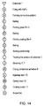
- the through holes 2 are filled with an electroconductive material 3, such as AgPd, as shown in Fig. 3 (Process step A of Fig. 14).
- a line shape conductive pattern 4 (Fig. 3, Fig. 4) which is connected with the electroconductive material 3, and on a reverse surface a round shape conductive pattern 4 (Fig. 3) connected with the electroconductive material 3, respectively, are formed by a thick film printing process (Process step B of Fig. 4).
- the conductive pattern 4 is comprised of an AgPd paste or an Ag paste.
- a mark 9 for location detection is also printed at two places on a diagonal of the substrate 1. And then, the conductive pattern 4 is baked (Process step C of Fig. 14).
- an insulating glass film 5 (Fig. 3, Fig. 5) is printed in a frame shape, and an insulating glass film 5 of square shape in the inner part (Fig. 5); on the reverse surface of substrate 1, an insulating glass film 5 (Fig. 3) is printed over substantially the whole surface excluding the conductive pattern 4 (Process step D of Fig. 14).
- the insulating glass film 5 is comprised of a crystallized glass. The insulating glass film 5 thus formed is effective to avoid the humidity sneaking into substrate 1, and the occurrence of migration with the conductive pattern 4 is also suppressed.
- the insulating glass film 5 is baked at a-temperature 850 °C (Process step E of Fig. 14).
- a coating film 6 (Fig. 1 - Fig. 3, Fig. 5) comprised of an amorphous glass is formed by means of printing process (Process step F of Fig. 14).
- the coating film 6 is baked at a temperature 600 °C (Process step G of Fig. 14).
- a substrate 1 is provided, on which surface the connecting areas 4a of conductive pattern 4 are exposed intermittently in a frame shape region.
- An electroconductive rubber piece (not shown) is pressed to the front surface of substrate 1, and a conductivity test electrode (not shown) is placed to touch on the round conductive pattern 4 formed on the rear surface of the substrate 1, for performing a conductivity test (Process step H of Fig. 14).
- a plurality of connecting areas 4a for connection with electrodes of an electronic component is disposed in the proximity with a small clearance to each other over the front surface of substrate 1. It is quite difficult to make each of the contacting areas 4a touch with a conductivity test electrode. Therefore, all the contacting areas 4a are short-circuited by pressing an electroconductive rubber piece on the surface.
- a round conductive pattern 4 coupled with the connecting area 4a via electroconductive material 3 is provided as shown in Fig. 3.
- the round conductive patterns 4 are placed scattered over the substrate 1, as shown in Fig. 6, with sufficient distance from adjacent ones. So, a conductivity test electrode may easily come into contact with the conductive pattern.
- the conductivity between the connecting area 4a on the front surface and the round conductive pattern 4 on the reverse surface may be tested by confirming the conductivity between two conductive patterns on the reverse surface. As soon as the conductivity test is finished, the electroconductive rubber piece provided on the front surface of substrate 1 and the conductivity test electrode placed on the reverse surface are removed.
- the front surface of substrate 1 undergoes a sand blasting treatment with SiC powder of 5 - 7 ⁇ m grain diameter (Process step I of Fig. 14).
- This treatment is effective with respect to the following function. Namely, a small portion of the electroconductive rubber piece which was pressed to the connecting area 4a, on which surface a protruding electrode 7a of IC 7 is to be connected in a subsequent process step, at the conductivity test inevitably remains sticking on the connecting area 4a. As the small portion sticking on the connecting area is hardly elctroconductive, a conductivity trouble may arise between the surface of connecting area 4a and the protruding electrode 7a when IC 7 is mounted the substrate. This is the reason why the sticking portion has to be removed.
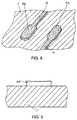
- the conductive pattern 4 before sand blasting treatment is roughened in the surface by the sand blasting to a state as shown in Fig. 8 and Fig. 9.
- the portion sticking on the surface of connecting area 4a is removed; as a result, the conductivity trouble between said connecting area 4a and protruding electrode 7a may be eliminated.
- the surface roughening treatment is effective also to enhance the connecting strength between connecting area 4a and IC 7.
- the dimensions of protruding electrode 7a locating under IC 7 is quite small, the surface roughening treatment applied on the corresponding connecting area 4a of conductive pattern 4 brings about an increased connecting surface area and an enhanced anchoring effect by the electroconductive adhesive 8.
- the protruding electrode 7a is connected firmly with the connecting area 4a.
- the roughened surface of connecting area 4a contributes to prevent the protruding electrode 7a from moving sidewise on the connecting surface 4a during mounting operation of IC 7. Thus the reliability in mounting is also improved.
- depth of the valley (a distance between a bottom of the valley and a top thereof) is not greater than 15 ⁇ m.
- the preferable thickness of the electroconductive adhesive 8 is approximately 15 ⁇ m. If the depth of the valley is greater than 15 ⁇ m, the electroconductive adhesive 8 may be mostly absorbed in the valley when volume of the adhesive 8 is small. This might cause an insufficient connecting strength between the protruding electrode 7a and the connecting area 4a.
- the conductive pattern 4 of the present exemplary embodiment has been formed by a thick film printing process. Therefore, it is easy to have the surface of connecting area 4a roughened to any desired surface condition through the control of material, grain size, etc. of abrasive and the speed of colliding against the surface of conductive pattern 4 during sand blasting treatment. There may be no risk of having a breakage in the connecting area 4a inviting a reduction of connecting surface area; contrary, even if a part of the connecting area 4a, for example, its central portion, had been formed protruded during the printing the sand blasting pushes the protrusion down to make the entire area substantially flat, as shown in Fig. 9.
- a dry etching process may be employed.
- the exposed surface of conductive pattern 4, the surface of coating film 6, the exposed surface of substrate 1 on which the connecting area 4a is disposed, and the surface of a mark 9 for location detection formed at a same process step for forming the conductive pattern 4, shown in Fig. 3 and Fig. 5, may be roughened too, in addition to the surface of connecting area 4a.
- the detection of location of substrate 1 is made by an optical system when mounting an IC 7, the roughened surface of mark 9 reflects less light, which contributes to an increased accuracy of location sensing.
- the IC 7 may be rightly mounted on substrate 1.
- IC 7 is mounted on the substrate by first printing the electroconductive adhesive 8 on the surface of connecting area 4a, and then bringing the protruding electrode 7a to make contact with the surface of connecting area 4a (Process step J of Fig. 14).
- the electroconductive adhesive 8 is then dried at a temperature 50 - 120 °C (Process step K of Fig. 14).
- a sealing resin 10 (Fig. 3) is injected between the substrate 1 and the IC 7 (Process step L of Fig. 14).
- the sealing resin 10 is cured at a temperature 120 - 150 °C (Process step M of Fig. 14).
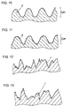
- the surface of coating film 6 (Fig. 5) locating underneath the IC 7 has already been roughened by sand blasting treatment, as shown in Fig. 10 and Fig. 11, when the sealing resin 10 is injected.
- the roughened surface provides a sort of capillary to help the sealing resin 10 go into a gap between IC 7 and substrate 1.
- the interlocating sealing resin 10 plays a role of anchoring the IC 7 firmly onto the roughened surface of coating film 6, in the succeeding step of curing.
- the circumferential area of substrate 1 outside the IC 7 has also been roughened by sand blasting treatment, as shown in Fig. 12 and Fig. 13; therefore, the adhesion strength of sealing resin 10 with the circumferential area is also increased by the anchoring effect.
- a plurality of substrates 1 is stuck on a plate 12 made of a metal or a ceramic using a double-faced adhesive tape 13 of a certain length as shown in Fig. 15, and then the roughening treatment is performed by blasting the abrasives along a direction of the length direction of tape 13 from a nozzle 14 against the substrates 1, as shown in Fig. 16.
- the substrates 1 stuck on the plate 12 are not swayed by the abrasives blasted from nozzle 14; therefore, the surface of connecting area 4a of a conductive pattern 14 on the substrate 1 and the surface of outer circumferential area of the substrate 1 may be surely roughened.
- Each of the substrates 1 shown in Fig. 15 and Fig. 16 has been provided out of a large-size substrate having splitting grooves formed thereon, which substrate is split along the grooves into pieces of individual substrate 1.
- a number of substrates 1 may be easily available in this way from a large-size substrate.
- a substrate 1 manufactured through the above procedure often bears a crack in the outer circumferential portion, which crack having been generated at the time when it was separated from the large-size substrate.
- the crack in the circumferential portion is liable to grow into a broken substrate 1 in the subsequent manufacturing steps.
- the crack is removed in advance by blasting abrasives from nozzle 14 to prevent occurrence of the broken substrate 1.
- the operating efficiency has been raised by performing the roughening treatments on the outer circumferential surface of substrate 1 and on the surface of connecting area 4a at a same time, in the present exemplary embodiment.
- the nozzle 14 sweeps over the plate 12 after a rectangular waveform, as shown in Fig. 16.
- the sweeping motion enables a small nozzle 14 to perform a substantially homogeneous roughening treatment on the plurality of substrates 1 disposed on plate 12.
- the surface roughening may be applied more homogeneously on the substrates. If the nozzle 14 is made to take in a second sweep a track that is different from that in a first sweep, the surface of plurality of substrates 1 disposed on plate 12 may be roughened sufficiently homogeneous even if the pattern of abrasives blasted from nozzle 14 was not uniform.
- a pair of sides 1a, among the total sides, of substrate 1 remains as the surface free of sticking. Therefore, the portion of the pair of sides 1a may easily be roughened by the abrasives blasted from nozzle 14. After the roughening treatment is over, the substrate 1 may be peeled off the plate 12 easily from the portion free of sticking.
- each of the substrates 1 may be stuck on plate 12 with a tape 13 of reduced size whose outer diameter is smaller than that of individual substrate 1.
- One of the methods is to rotate the plate 12 for approximately 90 degrees after the plate 12 is swept once by the nozzle 14, and then the plate 12 is swept again by the nozzle 14.
- the state of roughened surface of substrate 1 becomes resembled to that roughened by nozzle from both ode direction (for example, X direction) and the other direction (Y direction). In this way a surface may be roughened more homogeneously.
- nozzle 14 whose width of opening is larger than the width of substrate 1.
- Each of the substrates 1 may be roughened at each time for the entire surface. Thus a more homogeneous roughened surface may be obtained.
- the blasting of larger grain-size abrasives may roughen the surface of substrate 1 wildly, and break an imperfect conductive pattern 4 in advance for the prevention of possible rejects that might arise in the subsequent process steps.
- the re-treatment with the smaller grain-size abrasives eliminates any difficulty in mounting an electronic component on substrate 1.
- the substrates 1 may also be fixed on a plate 12 by disposing a plurality of substrates 1 on a plate 12 in a straight line arrangement providing a sort of substrates cluster, and then abrasives from nozzle 14 may be blasted against the substrates 1 after regulating the positioning of the substrates cluster at both ends in the length direction with a guide member.
- the surface of a plurality of substrates may receive the roughening treatment at one time.
- the abrasives may be blasted from under the substrate 1 by nozzle 14, as shown in Fig. 17. Namely, the plate 12 is reversed upside down so as the substrate 1 comes under the plate 12, and the nozzle 14 located under the substrate 1 blasts abrasives upward against the substrate 1. The abrasives and chip dusts of roughening fall downward, so it may be difficult for them to stay on the surface of substrate 1. As a result, occurrence of the connection rejects due to residuals staying between connecting area 4a and protruding electrode 7a may be suppressed.
- the surface of substrate 1, after being roughened by abrasives blasted from nozzle 14, is blown with a gas containing least oxygen.
- a gas containing least oxygen As the abrasives and chip dusts remaining after the roughening treatment are blown away from the substrate 1 by the gas, the occurrence of connection trouble between connecting area 4a and protruding electrode 7a due to such residuals may be suppressed.
- a liquid vessel 15 Provided at the bottom of a liquid vessel 15 is an ultrasonic oscillation element 16. Inside the liquid vessel 15, a container 17 made of wire frame is provided and a substrate 1 is placed flutterable in an individual storage sector 17a of the container 17. The vessel 15 is filled with a liquid containing no oxygen, for example, alcohol. By the ultrasonic cleaning the abrasives and chip dusts are removed from the surface of substrate 1.
- the surface of connecting area 4a of conductive pattern 4 is least oxidized, which contributes to suppress the occurrence of connection trouble between the connecting area 4a and the protruding electrode 7a of IC 7 due to surface oxidation.
- alcohol is used for the liquid, drying treatments after cleaning are easy because of its high volatility.
- a number of substrates 1 may be cleaned at once.
- a substrate 1 is disposed standing upright the abrasives and chip dusts fall under the substrate 1, and a high cleaning effect is obtainable.
- a substrate 1 is disposed flutterable in the individual storage sector 17a of container 17, the substrate 1 flutters during ultrasonic cleaning procedure to yield a still higher cleaning effect.
- a substrate 1 After being cleaned, with a gas containing least oxygen.
- a gas containing least oxygen By the gas blowing, substrate 1 dries up quickly, and oxidation of the surface of connecting area 4a is suppressed. Further, it is preferred that substrates 1 after drying are stored in an ambient free from the atmospheric air. By so doing, the surface of connecting area 4a under the storage may be prevented from getting materially oxidized. This contributes to eliminate a connection trouble with the protruding electrode 7a of IC 7 that might occur in a subsequent process step.
Landscapes
- Engineering & Computer Science (AREA)
- Microelectronics & Electronic Packaging (AREA)
- Manufacturing & Machinery (AREA)
- Electric Connection Of Electric Components To Printed Circuits (AREA)
- Manufacturing Of Printed Wiring (AREA)
- Structures Or Materials For Encapsulating Or Coating Semiconductor Devices Or Solid State Devices (AREA)
- Wire Bonding (AREA)
- Structures For Mounting Electric Components On Printed Circuit Boards (AREA)
Applications Claiming Priority (6)
| Application Number | Priority Date | Filing Date | Title |
|---|---|---|---|
| JP316767/97 | 1997-11-18 | ||
| JP31676797 | 1997-11-18 | ||
| JP31676797 | 1997-11-18 | ||
| JP10083365A JPH11214450A (ja) | 1997-11-18 | 1998-03-30 | 電子部品実装体とそれを用いた電子機器と電子部品実装体の製造方法 |
| JP8336598 | 1998-03-30 | ||
| JP83365/98 | 1998-03-30 |
Publications (2)
| Publication Number | Publication Date |
|---|---|
| EP0917191A2 true EP0917191A2 (de) | 1999-05-19 |
| EP0917191A3 EP0917191A3 (de) | 2000-05-24 |
Family
ID=26424402
Family Applications (1)
| Application Number | Title | Priority Date | Filing Date |
|---|---|---|---|
| EP98121864A Withdrawn EP0917191A3 (de) | 1997-11-18 | 1998-11-17 | Elektronische Bauelementeinheit, elektronischer Zusammenbau welcher diese Einheit anwendet, und Herstellungsverfahren für diese elektronische Bauelementeinheit |
Country Status (6)
| Country | Link |
|---|---|
| US (1) | US6792677B1 (de) |
| EP (1) | EP0917191A3 (de) |
| JP (1) | JPH11214450A (de) |
| KR (1) | KR100325566B1 (de) |
| CN (1) | CN1189929C (de) |
| TW (1) | TW410532B (de) |
Cited By (3)
| Publication number | Priority date | Publication date | Assignee | Title |
|---|---|---|---|---|
| WO2006012847A1 (de) * | 2004-07-29 | 2006-02-09 | Infineon Technologies Ag | Vertikales leistungshalbleiterbauteil mit einem halbleiterchip und verfahren zur herstellung desselben |
| US7138298B2 (en) | 1999-06-07 | 2006-11-21 | Rohm Co., Ltd. | Semiconductor chip with external connecting terminal |
| WO2007050166A1 (en) * | 2005-10-24 | 2007-05-03 | Hewlett-Packard Development Company, L.P. | Encapsulating electrical connections |
Families Citing this family (14)
| Publication number | Priority date | Publication date | Assignee | Title |
|---|---|---|---|---|
| US7059512B2 (en) * | 2002-11-06 | 2006-06-13 | Ricoh Company, Ltd. | Solder alloy material layer composition, electroconductive and adhesive composition, flux material layer composition, solder ball transferring sheet, bump and bump forming process, and semiconductor device |
| US20050048680A1 (en) * | 2003-08-29 | 2005-03-03 | Texas Instruments Incorporated | Printing one or more electrically conductive bonding lines to provide electrical conductivity in a circuit |
| JP4427374B2 (ja) * | 2004-04-05 | 2010-03-03 | アルプス電気株式会社 | プリント配線基板およびこの製造方法 |
| JP4729963B2 (ja) * | 2005-04-15 | 2011-07-20 | パナソニック株式会社 | 電子部品接続用突起電極とそれを用いた電子部品実装体およびそれらの製造方法 |
| KR100722647B1 (ko) | 2005-06-25 | 2007-05-28 | 삼성전기주식회사 | 몰딩된 전자부품 패키지를 내장한 기판의 제조방법 |
| CN103210703B (zh) * | 2010-09-13 | 2016-08-10 | Pst传感器(私人)有限公司 | 装配和封装分立电子元件 |
| JP5864954B2 (ja) * | 2011-08-26 | 2016-02-17 | 新光電気工業株式会社 | 基材 |
| JP2013232483A (ja) * | 2012-04-27 | 2013-11-14 | Koito Mfg Co Ltd | 回路基板及び回路基板の製造方法 |
| WO2015046977A1 (ko) * | 2013-09-27 | 2015-04-02 | 주식회사 엘지화학 | 고체 산화물 연료전지의 연료극 지지체 제조방법 및 고체 산화물 연료전지의 연료극 지지체 |
| CN104655561A (zh) * | 2014-12-31 | 2015-05-27 | 东莞美维电路有限公司 | 金手指镀层剥离检测方法 |
| CN107263972A (zh) | 2016-04-08 | 2017-10-20 | 优尔材料工业(深圳)有限公司 | 无机非金属与塑料的复合体及其制备方法 |
| DE102016224909B4 (de) * | 2016-12-14 | 2024-08-14 | Vitesco Technologies Germany Gmbh | Verfahren zur Herstellung einer Leiterplatte mit porösen oder rauen Zinnoberflächen |
| JP2018116037A (ja) * | 2017-01-13 | 2018-07-26 | 株式会社エンプラス | マーカ搭載用ユニットおよびその製造方法 |
| JP2026069981A (ja) * | 2024-10-15 | 2026-04-27 | 矢崎総業株式会社 | 電気接続ユニット |
Citations (1)
| Publication number | Priority date | Publication date | Assignee | Title |
|---|---|---|---|---|
| GB2265224A (en) * | 1992-03-20 | 1993-09-22 | Centalic Tech Dev Ltd | Testing printed circuit boards |
Family Cites Families (10)
| Publication number | Priority date | Publication date | Assignee | Title |
|---|---|---|---|---|
| US3762040A (en) * | 1971-10-06 | 1973-10-02 | Western Electric Co | Method of forming circuit crossovers |
| DE3608010A1 (de) * | 1986-03-11 | 1987-09-17 | Philips Patentverwaltung | Verfahren zum herstellen einer elektrisch leitenden klebverbindung |
| US4767049A (en) * | 1986-05-19 | 1988-08-30 | Olin Corporation | Special surfaces for wire bonding |
| JPH01166956A (ja) * | 1987-12-24 | 1989-06-30 | Shin Kobe Electric Mach Co Ltd | 金属ベース金属箔張積層板の製造法 |
| US4937653A (en) * | 1988-07-21 | 1990-06-26 | American Telephone And Telegraph Company | Semiconductor integrated circuit chip-to-chip interconnection scheme |
| JPH02308597A (ja) * | 1989-05-24 | 1990-12-21 | Asahi Chem Ind Co Ltd | 精細回路を有するセラミック基板の製法 |
| JPH0318826A (ja) * | 1989-06-15 | 1991-01-28 | Matsushita Electric Ind Co Ltd | 液晶表示素子 |
| US5816478A (en) * | 1995-06-05 | 1998-10-06 | Motorola, Inc. | Fluxless flip-chip bond and a method for making |
| DE19622684A1 (de) * | 1996-06-05 | 1997-12-11 | Siemens Ag | Verfahren zur Herstellung mechanisch fester Klebstoffverbindungen zwischen Oberflächen |
| JPH10112479A (ja) * | 1996-10-07 | 1998-04-28 | Fuji Xerox Co Ltd | 基板の接続方法 |
-
1998
- 1998-03-30 JP JP10083365A patent/JPH11214450A/ja active Pending
- 1998-10-20 TW TW087117312A patent/TW410532B/zh not_active IP Right Cessation
- 1998-11-17 EP EP98121864A patent/EP0917191A3/de not_active Withdrawn
- 1998-11-18 US US09/195,595 patent/US6792677B1/en not_active Expired - Fee Related
- 1998-11-18 CN CNB981226612A patent/CN1189929C/zh not_active Expired - Fee Related
- 1998-11-18 KR KR1019980049365A patent/KR100325566B1/ko not_active Expired - Fee Related
Patent Citations (1)
| Publication number | Priority date | Publication date | Assignee | Title |
|---|---|---|---|---|
| GB2265224A (en) * | 1992-03-20 | 1993-09-22 | Centalic Tech Dev Ltd | Testing printed circuit boards |
Cited By (7)
| Publication number | Priority date | Publication date | Assignee | Title |
|---|---|---|---|---|
| US7138298B2 (en) | 1999-06-07 | 2006-11-21 | Rohm Co., Ltd. | Semiconductor chip with external connecting terminal |
| KR100665777B1 (ko) * | 1999-06-07 | 2007-01-09 | 로무 가부시키가이샤 | 반도체장치 및 그 제조방법 |
| US7262490B2 (en) | 1999-06-07 | 2007-08-28 | Rohm Co., Ltd. | Semiconductor chip with external connecting terminal |
| US7339264B2 (en) | 1999-06-07 | 2008-03-04 | Rohm Co., Ltd. | Semiconductor chip with external connecting terminal |
| WO2006012847A1 (de) * | 2004-07-29 | 2006-02-09 | Infineon Technologies Ag | Vertikales leistungshalbleiterbauteil mit einem halbleiterchip und verfahren zur herstellung desselben |
| WO2007050166A1 (en) * | 2005-10-24 | 2007-05-03 | Hewlett-Packard Development Company, L.P. | Encapsulating electrical connections |
| US7691675B2 (en) | 2005-10-24 | 2010-04-06 | Hewlett-Packard Development Company, L.P. | Encapsulating electrical connections |
Also Published As
| Publication number | Publication date |
|---|---|
| KR100325566B1 (ko) | 2002-04-17 |
| JPH11214450A (ja) | 1999-08-06 |
| KR19990045360A (ko) | 1999-06-25 |
| US6792677B1 (en) | 2004-09-21 |
| TW410532B (en) | 2000-11-01 |
| CN1189929C (zh) | 2005-02-16 |
| EP0917191A3 (de) | 2000-05-24 |
| CN1219100A (zh) | 1999-06-09 |
Similar Documents
| Publication | Publication Date | Title |
|---|---|---|
| US6792677B1 (en) | Method of manufacturing an electronic component unit | |
| JP3123483B2 (ja) | プローブカード及びプローブカード形成方法 | |
| JP2007514177A (ja) | 基板の清掃装置及び清掃方法、フラットディスプレイパネル、電子部品の実装装置及び実装方法 | |
| US20080036479A1 (en) | Probe and Method of Manufacturing Probe | |
| JP4202606B2 (ja) | 湿度測定のための装置 | |
| JP2796070B2 (ja) | プローブカードの製造方法 | |
| JP2002124319A (ja) | 異方導電性フィルムおよびそれを用いた半導体素子または電子部品の検査方法 | |
| US5120591A (en) | Conductive pattern board and method for producing the same | |
| JPH10132855A (ja) | Ic検査用プローブカード | |
| JP2001119131A (ja) | 電子部品実装体とそれを用いた電子機器と電子部品実装体の製造方法 | |
| JP2001119131A5 (de) | ||
| JPH10104271A (ja) | コンタクトプローブ及びその製造方法 | |
| JP2005026265A (ja) | クリーニング機構付きプローバ及びそのクリーニング方法 | |
| JP2003121469A (ja) | プローブの製造方法及びプローブカードの製造方法 | |
| JP3252765B2 (ja) | プリント配線板の検査装置 | |
| JP4210002B2 (ja) | コンタクトプローブ及びコンタクトピンの研磨方法 | |
| JP4308371B2 (ja) | コンタクトプローブ及びプローブ装置 | |
| JP3792580B2 (ja) | コンタクトプローブおよびその製造方法 | |
| JP2001099882A (ja) | プリント配線板の検査装置 | |
| JP3794217B2 (ja) | 液晶装置の製造方法 | |
| JPH09281145A (ja) | 異方性導電材を有する検査治具及びその製造方法 | |
| JP2002148279A (ja) | 電気検査用同軸プローブ | |
| JP3269492B2 (ja) | プリント配線板の検査装置および検査方法 | |
| JPS63262849A (ja) | プロ−ブカ−ド | |
| JP2001153922A (ja) | 検査用ソケット |
Legal Events
| Date | Code | Title | Description |
|---|---|---|---|
| PUAI | Public reference made under article 153(3) epc to a published international application that has entered the european phase |
Free format text: ORIGINAL CODE: 0009012 |
|
| AK | Designated contracting states |
Kind code of ref document: A2 Designated state(s): DE FR GB |
|
| AX | Request for extension of the european patent |
Free format text: AL;LT;LV;MK;RO;SI |
|
| PUAL | Search report despatched |
Free format text: ORIGINAL CODE: 0009013 |
|
| AK | Designated contracting states |
Kind code of ref document: A3 Designated state(s): AT BE CH CY DE DK ES FI FR GB GR IE IT LI LU MC NL PT SE |
|
| AX | Request for extension of the european patent |
Free format text: AL;LT;LV;MK;RO;SI |
|
| 17P | Request for examination filed |
Effective date: 20001121 |
|
| AKX | Designation fees paid |
Free format text: DE FR GB |
|
| 17Q | First examination report despatched |
Effective date: 20040203 |
|
| RAP1 | Party data changed (applicant data changed or rights of an application transferred) |
Owner name: PANASONIC CORPORATION |
|
| STAA | Information on the status of an ep patent application or granted ep patent |
Free format text: STATUS: THE APPLICATION IS DEEMED TO BE WITHDRAWN |
|
| 18D | Application deemed to be withdrawn |
Effective date: 20090827 |