EP0917197A2 - Integrierte Schaltung hoher Frequenz und Verfahren zur Herstellung - Google Patents
Integrierte Schaltung hoher Frequenz und Verfahren zur Herstellung Download PDFInfo
- Publication number
- EP0917197A2 EP0917197A2 EP98121227A EP98121227A EP0917197A2 EP 0917197 A2 EP0917197 A2 EP 0917197A2 EP 98121227 A EP98121227 A EP 98121227A EP 98121227 A EP98121227 A EP 98121227A EP 0917197 A2 EP0917197 A2 EP 0917197A2
- Authority
- EP
- European Patent Office
- Prior art keywords
- high frequency
- integrated circuit
- parts
- frequency integrated
- circuit
- Prior art date
- Legal status (The legal status is an assumption and is not a legal conclusion. Google has not performed a legal analysis and makes no representation as to the accuracy of the status listed.)
- Withdrawn
Links
Images

Classifications
-
- H—ELECTRICITY
- H05—ELECTRIC TECHNIQUES NOT OTHERWISE PROVIDED FOR
- H05K—PRINTED CIRCUITS; CASINGS OR CONSTRUCTIONAL DETAILS OF ELECTRIC APPARATUS; MANUFACTURE OF ASSEMBLAGES OF ELECTRICAL COMPONENTS
- H05K1/00—Printed circuits
- H05K1/18—Printed circuits structurally associated with non-printed electric components
- H05K1/182—Printed circuits structurally associated with non-printed electric components associated with components mounted in printed circuit boards [PCB], e.g. insert-mounted components [IMC]
- H05K1/184—Printed circuits structurally associated with non-printed electric components associated with components mounted in printed circuit boards [PCB], e.g. insert-mounted components [IMC] associated with components inserted in holes through the PCBs and wherein terminals of the components are connected to printed contacts on the walls of the holes or at the edges thereof or protruding over or into the holes
-
- H—ELECTRICITY
- H05—ELECTRIC TECHNIQUES NOT OTHERWISE PROVIDED FOR
- H05K—PRINTED CIRCUITS; CASINGS OR CONSTRUCTIONAL DETAILS OF ELECTRIC APPARATUS; MANUFACTURE OF ASSEMBLAGES OF ELECTRICAL COMPONENTS
- H05K1/00—Printed circuits
- H05K1/16—Printed circuits incorporating printed electric components, e.g. printed resistors, capacitors or inductors
- H05K1/165—Printed circuits incorporating printed electric components, e.g. printed resistors, capacitors or inductors incorporating printed inductors
-
- H—ELECTRICITY
- H05—ELECTRIC TECHNIQUES NOT OTHERWISE PROVIDED FOR
- H05K—PRINTED CIRCUITS; CASINGS OR CONSTRUCTIONAL DETAILS OF ELECTRIC APPARATUS; MANUFACTURE OF ASSEMBLAGES OF ELECTRICAL COMPONENTS
- H05K1/00—Printed circuits
- H05K1/18—Printed circuits structurally associated with non-printed electric components
- H05K1/182—Printed circuits structurally associated with non-printed electric components associated with components mounted in printed circuit boards [PCB], e.g. insert-mounted components [IMC]
- H05K1/185—Printed circuits structurally associated with non-printed electric components associated with components mounted in printed circuit boards [PCB], e.g. insert-mounted components [IMC] associated with components encapsulated in the insulating substrate of the PCBs; associated with components incorporated in internal layers of multilayer circuit boards
-
- H—ELECTRICITY
- H10—SEMICONDUCTOR DEVICES; ELECTRIC SOLID-STATE DEVICES NOT OTHERWISE PROVIDED FOR
- H10W—GENERIC PACKAGES, INTERCONNECTIONS, CONNECTORS OR OTHER CONSTRUCTIONAL DETAILS OF DEVICES COVERED BY CLASS H10
- H10W44/00—Electrical arrangements for controlling or matching impedance
- H10W44/20—Electrical arrangements for controlling or matching impedance at high-frequency [HF] or radio frequency [RF]
-
- H—ELECTRICITY
- H05—ELECTRIC TECHNIQUES NOT OTHERWISE PROVIDED FOR
- H05K—PRINTED CIRCUITS; CASINGS OR CONSTRUCTIONAL DETAILS OF ELECTRIC APPARATUS; MANUFACTURE OF ASSEMBLAGES OF ELECTRICAL COMPONENTS
- H05K1/00—Printed circuits
- H05K1/02—Details
- H05K1/03—Use of materials for the substrate
- H05K1/0306—Inorganic insulating substrates, e.g. ceramic, glass
-
- H—ELECTRICITY
- H05—ELECTRIC TECHNIQUES NOT OTHERWISE PROVIDED FOR
- H05K—PRINTED CIRCUITS; CASINGS OR CONSTRUCTIONAL DETAILS OF ELECTRIC APPARATUS; MANUFACTURE OF ASSEMBLAGES OF ELECTRICAL COMPONENTS
- H05K1/00—Printed circuits
- H05K1/02—Details
- H05K1/09—Use of materials for the conductive, e.g. metallic pattern
- H05K1/092—Dispersed materials, e.g. conductive pastes or inks
-
- H—ELECTRICITY
- H05—ELECTRIC TECHNIQUES NOT OTHERWISE PROVIDED FOR
- H05K—PRINTED CIRCUITS; CASINGS OR CONSTRUCTIONAL DETAILS OF ELECTRIC APPARATUS; MANUFACTURE OF ASSEMBLAGES OF ELECTRICAL COMPONENTS
- H05K2201/00—Indexing scheme relating to printed circuits covered by H05K1/00
- H05K2201/08—Magnetic details
- H05K2201/083—Magnetic materials
- H05K2201/086—Magnetic materials for inductive purposes, e.g. printed inductor with ferrite core
-
- H—ELECTRICITY
- H05—ELECTRIC TECHNIQUES NOT OTHERWISE PROVIDED FOR
- H05K—PRINTED CIRCUITS; CASINGS OR CONSTRUCTIONAL DETAILS OF ELECTRIC APPARATUS; MANUFACTURE OF ASSEMBLAGES OF ELECTRICAL COMPONENTS
- H05K2201/00—Indexing scheme relating to printed circuits covered by H05K1/00
- H05K2201/10—Details of components or other objects attached to or integrated in a printed circuit board
- H05K2201/10227—Other objects, e.g. metallic pieces
- H05K2201/10416—Metallic blocks or heatsinks completely inserted in a PCB
-
- H—ELECTRICITY
- H05—ELECTRIC TECHNIQUES NOT OTHERWISE PROVIDED FOR
- H05K—PRINTED CIRCUITS; CASINGS OR CONSTRUCTIONAL DETAILS OF ELECTRIC APPARATUS; MANUFACTURE OF ASSEMBLAGES OF ELECTRICAL COMPONENTS
- H05K2201/00—Indexing scheme relating to printed circuits covered by H05K1/00
- H05K2201/10—Details of components or other objects attached to or integrated in a printed circuit board
- H05K2201/10613—Details of electrical connections of non-printed components, e.g. special leads
- H05K2201/10621—Components characterised by their electrical contacts
- H05K2201/10643—Disc shaped leadless component
Definitions
- the present invention relates to a micro wave integrated circuit (MIC) having a plurality of circuit parts mounted on a ceramic substrate and a method for manufacturing the same integrated circuit.
- the present invention is utilized in a communication equipment, a radar, a measuring equipment or other equipments.
- the present invention is utilized in a filter circuit, an isolator, a transmission/receiving separating circuit, an antenna circuit or other circuits of these equipments.
- the present invention was developed for utilization thereof in a high frequency circuit operating at a frequency exceeding 10 GHz, the utilizing frequency is not limited thereto and the present invention can be utilized in a circuit operating at a frequency not higher than 10 GHz.
- a technique for forming a micro wave integrated circuit having a plurality of circuit parts mounted on a ceramic substrate by soldering or ribbon or wire connection has been known. Although it is usual to form conductors of a circulator, among the circuit parts mounted on a ceramic substrate, on a soft ferrite substrate, Japanese Patent Application Laid-open No. Hei 61-288486 discloses a technique in which holes are formed in a green sheet of an alumina substrate which is to be sintered at low temperature, ferrite parts are fitted in these holes and the green sheet is sintered to fixedly secure the ferrite parts in the holes.
- This technique is useful technique in mounting ferrite parts in a ceramic substrate and the present invention is based on this technique.
- this technique is to form a circulator part by mounting a ferrite unit on a low temperature sintered alumina substrate and does not suggest a technique for arranging a plurality of mutually related circuit parts on a low temperature sintered alumina substrate to unify them as an integrated circuit.
- the disclosed technique does not suggest a use of hard ferrite as the ferrite material and a magnetization of the hard ferrite correspondingly to a circuit characteristics after sintering.
- Japanese Patent Application Laid-open No. Hei 6-334413 of the same assignee as that of the present invention discloses a technique for unifying a high frequency filter as a monolithic micro wave integrated circuit.
- an insulating film is formed on a surface of a semiconductor substrate and a conductor lines are formed on the insulating film.
- a dielectric resonator is mounted in the vicinity of the conductor lines. The dielectric resonator is fitted in a recess formed in the insulating film.
- a high frequency band exceeding 10 GHz has being used in various equipments.
- a frequency of an automobile radar or a distance meter is assigned to a 60 GHz band or a 70 GHz band. Therefore, in view of a limited space in which such device is mounted, a technique for mass-producing a compact high frequency integrated circuit having uniform characteristics at low cost is required.
- an area for connecting such parts as a circulator, high frequency filter and MMIC, etc. is necessary, with which there is a limitation in reducing the size of device.
- the conventional technique is basically superior in forming a high frequency filter integrally with the MMIC.
- integration of a conventional circulator with MMIC is impossible in principle since the conventional circulator requires an external magnet.
- parts themselves have stable characteristics. Even if such parts are obtained, loss which can not be considered in design stage of the device may occur in connecting portions of the parts and it is impossible to control such loss, so that there may occur variation of characteristics between substrates. Therefore, it is necessary to regulate the characteristics of the device after assembled, the number of working steps is increased and skilled workers are necessary for the regulation of characteristics of the device.
- the present invention was made in view of the above background and has an object to provide a micro wave integrated circuit (MIC) including dielectric parts and magnetic parts both formed on a single substrate and a method for manufacturing the same.
- MIC micro wave integrated circuit
- Another object of the present invention is to provide a reliable high frequency integrated circuit having substantially no power loss at connecting points which is the problem in the structure in which individual parts are connected and a method for manufacturing the same high frequency integrated circuit.
- Another object of the present invention is to provide a high frequency integrated circuit which has a stable characteristics and is capable of being manufactured uniformly and a method for manufacturing the same high frequency integrated circuit.
- Another object of the present invention is to provide a high frequency integrated circuit capable of being manufactured with a small number of manufacturing steps and a method of manufacturing the same high frequency integrated circuit.
- a further object of the present invention is to provide a high frequency integrated circuit which can be mass-produced at low cost and a method of manufacturing the same high frequency integrated circuit.
- Another object of the present invention is to provide a high frequency integrated circuit which is suitable for use in designing and manufacturing a filter or an antenna circuit which can be utilized in several tens GHz frequency band and a method for manufacturing the same high frequency integrated circuit.
- a further object of the present invention is to provide a high frequency integrated circuit whose electric characteristics can be reversibly regulated while monitoring the characteristics thereof after manufactured and a method for manufacturing the same high frequency integrated circuit.
- a high frequency integrated circuit is featured by having a structure in which magnetic parts or magnetic parts and dielectric parts are unified in a single integrated circuit substrate and in which two or more of these circuit parts form a desired high frequency characteristics. That is, a plurality of parts constructing an isolator, a circulator or a filter are constituted as a circuit having a high frequency characteristics as a whole. A conductor pattern is formed on a surface of the ceramic substrate as lead lines of the circuit or micro strip lines.
- the magnetic parts may be of hard ferrite.
- the hard ferrite can be utilized as a constructive element of a circulator or an isolator.
- the dielectric parts can be utilized as constructive elements of a high frequency filter.
- the dielectric substrate may be of organic material and, particularly, polytetrafluoroethylene is a suitable material thereof.
- the dielectric substrate is preferably a ceramic substrate.
- a method for manufacturing a high frequency integrated circuit which is featured by comprising, in a case where the dielectric substrate is a glass ceramic substrate, the steps of forming a plurality of holes in a green sheet of the glass ceramic, fitting circuit parts in the respective holes, forming the ceramic substrate by sintering the green sheet at a temperature not high than a temperature at which the circuit parts are deformed and not lower than a sintering temperature of the green sheet and fixedly securing the circuit parts in the ceramic substrate by utilizing the shrinking nature of the holes during the sintering process of the ceramic substrate.
- the circuit pats include magnetic parts and dielectric parts and these parts are unified in a single substrate.
- the sintering temperature of the ceramic substrate is preferably in a range from 800°C to 1200°C.
- Height of the circuit part is not smaller than a thickness of the ceramic substrate and the hole is circular.
- An outer configuration of at least a portion of the circuit part is preferably a circular rod.
- the sintering temperature of the green sheet is not higher than the sintering temperature of the hard ferrite and the magnetic parts of hard ferrite are magnetized by applying magnetic field thereto after the sintering of the ceramic substrate.
- Curie temperature of hard ferrite is within a range from 400°C to 700°C depending upon the nature thereof and the magnetizing step is preferably performed during a cooling period for cooling the substrate from about Curie temperature to room temperature after the sintering of the ceramic substrate is completed. It is, of course, possible to perform the magnetization or demagnetization of the magnetic parts or to regulate the magnetized state after the ceramic substrate is cooled to room temperature.
- the electric characteristics of the integrated circuit is preferably regulated while monitoring it by regulating magnetic field applied to the magnetic parts of hard ferrite.
- a plurality of holes are formed in the glass ceramic substrate in a green sheet state before sintering by punching and the circuit parts are fitted in the respective holes. Then, the substrate is sintered.
- the holes By forming the holes by punching, the holes can be in a uniform and precise mutual positional relation. Since the green sheet is shrunken by sintering, the mutual positional relation of the holes is regulated by testing a plurality of samples such that the final configuration of the green sheet after sintering becomes a desired one. Once the mutual positional relation of the holes is regulated, it is possible to produce a large number of integrated circuits having identical configuration without necessity of regulating it individually.
- the size of hole formed in the green sheet is also regulated by testing a plurality of samples such that the magnetic parts and the dielectric parts are rigidly secured to the holes after sintering. Once the size of hole is regulated, it is possible to produce a large number of integrated circuits uniformly.
- Height of the circuit part is preferably equal to or larger than the thickness of the substrate.
- the height of the magnetic part is preferably the same as the thickness of the substrate, since it is usual to form a conductor between the magnetic part and the substrate and the characteristics of the integrated circuit may be degraded if there is a step in the conductor.
- the height of the dielectric part is larger than the thickness of the substrate, it is also possible to machine it. In such case, the freedom of configuration of the part becomes large and it becomes possible to design various circuits.
- the outer configuration of the circuit part may be other than circular rod, such as ellipsoidal. In such case, the number of tests to be performed in order to make the firm tightening optimal may be increased.
- the external magnet becomes unnecessary.
- an isolator or a circulator is realized by applying magnetic field to a magnetic element thereof by the external magnet in a high frequency integrated circuit operating in a frequency band of several tens GHz
- the magnetic field may influence other elements close to the aimed magnetic element since the integrated circuit is small and the inter-element distance is small, so that the mutual relation becomes complex, causing the design thereof to be difficult.
- the hard ferrite the influence of magnetic field on other elements is minimized and it becomes possible to realize a desired characteristics by a relatively simple design.
- the sintering temperature of the green sheet should be selected such that it changes the natures of the magnetic parts, particularly, the hard ferrite. According to experiments conducted by the inventors, it has been found that, even in a case where the sintering is performed at a temperature equal to or higher than Curie temperature of hard ferrite, a desired characteristics can be obtained by lowering temperature after the sintering is completed and regulating the magnetic orientation again by applying magnetic field to the hard ferrite when the temperature of the hard ferrite becomes about the Curie temperature or lower than the Curie temperature.
- the temperature in the sintering step and the temperature in the magnetizing step are selected according to the nature of the hard ferrite. It is not always necessary to set the sintering temperature equal to or higher than the Curie temperature of hard ferrite.
- the magnetization When the magnetization is performed after the sintering is completed, it may be possible to magnetize after the sample temperature becomes room temperature. However, it is easily possible to magnetize the magnetic part to a desired value when the magnetization is performed while lowering the temperature from a relatively high temperature. It is further possible to change the magnetizing state while monitoring the characteristics of the high frequency circuit by operating the high frequency circuit after magnetized once.
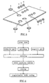
- Fig. 1 is a perspective view showing a whole construction of a high frequency integrated circuit according to an embodiment of the present invention.
- an input/output circuit of a radar transmitter/receiver is formed on a glass ceramic substrate of a size 18 X 11 X 0.3 mm.
- the input/output circuit of this radar transmitter/receiver is mounted on a front portion of a car and adapted to measure a distance between the car and a preceding car.
- the frequency in 60 ⁇ 70 GHz band (wavelength 4.3 - 5.0 mm) is assigned to such automobile radar.
- a dielectric part 2 As shown in Fig. 1, a dielectric part 2, two magnetic parts 3 and two sets of three dielectric parts 4 are buried in a glass ceramic substrate 1. Further, micro strip lines L and electrodes M of a metal, that is, gold, are also formed on a surface of the substrate.
- a metal that is, gold
- Fig. 2 is an equivalent circuit of the embodiment shown in Fig. 1.
- a portion of the circuit indicated by MIC in Fig. 2 is an integrated circuit formed on the substrate shown in Fig. 1.
- electromagnetic wave in 60 GHz band generated by a transmitter porion X is supplied to the micro strip lines L, a spurious wave thereof is removed by a band-pass filter F and supplied to a first terminal of a circulator C.
- the circulator C supplies the signal at its first terminal to an antenna A through a second terminal thereof. This signal from the antenna A is transmitted as electromagnetic wave.
- a receiving electromagnetic wave (reflected wave in a case of a radar) input to the antenna A is input to the second terminal of the circulator C and output to a third terminal thereof
- a first terminal of an isolator I is connected to the third terminal of the circulator C.
- the isolator I outputs the signal input to the first terminal to a second terminal thereof.
- a terminating resistor R having a value equal to a characteristics impedance of this circuit is connected to a third terminal of the isolator I.
- Noise component of the output signal at the second terminal of the isolator I is removed by another band-pass filter F, passes through the micro strip lines L and is supplied to an input terminal of a receiver portion RX.
- the circulator C supplies the signal at its first terminal to the second terminal thereof and does not supply the signal at the second terminal to the first terminal.
- the circulator C supplies the signal at its second terminal to the third terminal thereof and does not supply the signal at the third terminal to the second terminal.
- the isolator I supplies the signal at its first terminal to the second terminal.
- the signal at the second terminal of the isolator I is absorbed by the terminating resistor R and can not be supplied to the first terminal.
- Such working of the circulator C and the isolator I are realized by the magnetic parts as well known.
- Each of the circulator C and the isolator I shown in Fig. 2 is formed by providing a metal electrode on one of the magnetic parts 3.
- the antenna A is formed by forming a metal electrode on the dielectric part 2.
- the band-pass filter F is formed by one set of three dielectric parts 4.
- the terminating resistor R is formed by a resistance member provided on the surface of the substrate 1.
- Fig. 3 is a perspective view illustrating an assembling of the magnetic parts and the dielectric parts to a green sheet of the high frequency integrated circuit shown in Fig. 1 and Fig. 4 is a flowchart of a manufacture of the high frequency integrated circuit of the present invention.
- the glass ceramic substrate 1' in the form of a green sheet before sintering is punched to form holes and a circular ceramic dielectric rod as the dielectric part 2, circular hard ferrite rods as the magnetic parts 3 and circular ceramic dielectric rods as the dielectric parts 4 are fitted in the holes.
- the green sheet is sintered as shown in Fig. 4.
- the sintering temperature of the green sheet is lower than the sintering temperature of the hard ferrite.
- the sintering temperature of the green sheet is controlled to about 870°C.
- a conductor pattern of gold paste is printed on the surface of the glass ceramic substrate 1 by using a printing mask and the pattern is close adhered to the substrate surface and surfaces of the magnetic and dielectric parts by baking it at about 850°C.
- the substrate is naturally cooled in air and, when its surface temperature becomes about 600°C, magnetic field is applied to the magnetic parts 3 to magnetize them while being cooled.
- a plurality of the high frequency integrated circuits each prepared as mentioned above were acceptable in physical structure.
- ripple of the frequency-gain characteristics in the pass band is reduced by about 1 ⁇ 2 dB compared with the conventional case in which the dielectric elements are arranged by using adhesive and, thus, the pass band characteristics is flattened.
- the isolation band width was 2.5 GHz ⁇ 1.9 GHz for 5 samples whose metal conductor sizes were changed such that the operating center frequency of the circulator becomes in a range from 55 GHz to 64 GHz.
- the substrate 1 of the high frequency integrated circuit shown in Fig. 1 is of not glass ceramic but an organic material will be described.
- the circuit construction and operation are the same as those mentioned previously and, therefore, details thereof are omitted for avoidance of duplication.
- holes each having a diameter larger than a diameter of a cylindrical part to be buried in a substrate of polytetrafluoroethylene by about 0.05 ⁇ 0.1 mm are formed in the substrate.
- Adhesive is applied to inner walls of these holes by painting and magnetic parts and/or dielectric parts are fitted in and secured to the holes.
- metal conductors are formed on one surface of the substrate by plating such that the positional relation of the respective parts becomes desirable.
- magnetic parts are attached on a metal foil by using electrically conductive adhesive and dielectric parts are attached thereon by using an electrically conductive adhesive or an electrically insulating adhesive.
- a height of the dielectric part is made equal to or larger than a height of the magnetic part.
- An organic resin is painted on the surface of the metal foil on which the magnetic parts and the dielectric parts are attached to a thickness equal to the height of the magnetic parts and the organic substrate is formed by hardening the organic resin. Thereafter, metal conductors are formed on the surface of the substrate by plating such that a desired positional relation between the respective parts is obtained.
- holes each having a diameter larger than a diameter of a cylindrical part to be buried in an organic substrate by about 0.05 ⁇ 0.1 mm are formed in the substrate.
- magnetic parts are attached on a metal foil by using electrically conductive adhesive and dielectric parts are attached thereon by using an electrically conductive adhesive or an electrically insulating adhesive.
- a height of the dielectric part is made equal to or larger than a height of the magnetic part.
- the parts attached to the metal foil are inserted into the holes, respectively, from one of surfaces of the organic substrate and the metal foil is adhered to the surface of the substrate by using an adhesive.
- the thickness of the substrate is selected such that surfaces of the magnetic parts become coplanar with the other surface of the substrate. Thereafter, metal conductors are formed on the other surface of the substrate by plating such that a desired positional relation between the respective parts is obtained.
- the present invention it is possible to realize a high frequency integrated circuit capable of being used in a frequency region of 60 to 70 GHz band.
- the high frequency integrated circuit according to the present can provide uniform and stable characteristics and, when the present invention is applied to a mass-production of high frequency integrated circuit, it is possible to manufacture the high frequency integrated circuit at low cost.
- the structure in which magnetization is performed for hard ferrite parts buried in a dielectric substrate without using external magnet is very effective.
Landscapes
- Engineering & Computer Science (AREA)
- Microelectronics & Electronic Packaging (AREA)
- Non-Reversible Transmitting Devices (AREA)
- Structures For Mounting Electric Components On Printed Circuit Boards (AREA)
- Control Of Motors That Do Not Use Commutators (AREA)
- Transceivers (AREA)
- Shielding Devices Or Components To Electric Or Magnetic Fields (AREA)
- Ceramic Products (AREA)
- Waveguides (AREA)
Applications Claiming Priority (3)
| Application Number | Priority Date | Filing Date | Title |
|---|---|---|---|
| JP306011/97 | 1997-11-07 | ||
| JP30601197 | 1997-11-07 | ||
| JP30601197A JP3149831B2 (ja) | 1997-11-07 | 1997-11-07 | 高周波集積回路およびその製造方法 |
Publications (2)
| Publication Number | Publication Date |
|---|---|
| EP0917197A2 true EP0917197A2 (de) | 1999-05-19 |
| EP0917197A3 EP0917197A3 (de) | 2000-09-20 |
Family
ID=17952014
Family Applications (1)
| Application Number | Title | Priority Date | Filing Date |
|---|---|---|---|
| EP98121227A Withdrawn EP0917197A3 (de) | 1997-11-07 | 1998-11-06 | Integrierte Schaltung hoher Frequenz und Verfahren zur Herstellung |
Country Status (3)
| Country | Link |
|---|---|
| US (1) | US6504444B1 (de) |
| EP (1) | EP0917197A3 (de) |
| JP (1) | JP3149831B2 (de) |
Cited By (6)
| Publication number | Priority date | Publication date | Assignee | Title |
|---|---|---|---|---|
| WO2002067640A1 (en) * | 2001-02-16 | 2002-08-29 | Koninklijke Philips Electronics N.V. | Electronic device and method of manufacturing the same |
| WO2002078120A1 (en) * | 2001-03-23 | 2002-10-03 | Telefonaktiebolaget Lm Ericsson (Publ) | Circulator and network |
| WO2004055936A1 (en) * | 2002-12-17 | 2004-07-01 | Philips Intellectual Property & Standards Gmbh | Non-reciprocal circuit element |
| WO2005025001A1 (en) * | 2003-09-03 | 2005-03-17 | Raytheon Company | Embedded rf vertical interconnect for flexible conformal antenna |
| CN104577281A (zh) * | 2015-01-21 | 2015-04-29 | 南京大学 | 基于基片集成波导加载铁氧体的微波隔离器 |
| CN112366437A (zh) * | 2020-10-16 | 2021-02-12 | 武汉心浩智能科技有限公司 | 一种环行器的装配工艺 |
Families Citing this family (15)
| Publication number | Priority date | Publication date | Assignee | Title |
|---|---|---|---|---|
| US20050107612A1 (en) * | 2002-12-30 | 2005-05-19 | Dr. Reddy's Laboratories Limited | Process for preparation of montelukast and its salts |
| US7057560B2 (en) * | 2003-05-07 | 2006-06-06 | Agere Systems Inc. | Dual-band antenna for a wireless local area network device |
| US7239266B2 (en) * | 2004-08-26 | 2007-07-03 | Honeywell International Inc. | Radar altimeter |
| JP2006351627A (ja) * | 2005-06-13 | 2006-12-28 | Fdk Corp | 永久磁石の多極着磁装置 |
| JP4873300B2 (ja) * | 2006-06-21 | 2012-02-08 | 日立金属株式会社 | 携帯通信機器 |
| US7687014B2 (en) * | 2008-03-26 | 2010-03-30 | Skyworks Solutions, Inc. | Co-firing of magnetic and dielectric materials for fabricating composite assemblies for circulators and isolators |
| US8344955B2 (en) | 2010-01-08 | 2013-01-01 | Nokia Corporation | Integrated antenna with e-flex technology |
| US8716603B2 (en) | 2010-11-24 | 2014-05-06 | Nokia Corporation | Printed wiring board with dielectric material sections having different dissipation factors |
| EP2975687B1 (de) | 2013-03-15 | 2022-10-05 | NEC Corporation | Duplexer mit in-band-filtern und out-of-band-filtern, die mit zirkulatoren verbunden sind |
| JP6672904B2 (ja) * | 2016-03-08 | 2020-03-25 | 日本電気株式会社 | 位置決め装置および位置決め方法 |
| US20180166763A1 (en) | 2016-11-14 | 2018-06-14 | Skyworks Solutions, Inc. | Integrated microstrip and substrate integrated waveguide circulators/isolators formed with co-fired magnetic-dielectric composites |
| JP7115941B2 (ja) * | 2017-09-08 | 2022-08-09 | スカイワークス ソリューションズ,インコーポレイテッド | 複合材料の形成方法、及び無線周波数アイソレータ又はサーキュレータの形成方法 |
| US11603333B2 (en) | 2018-04-23 | 2023-03-14 | Skyworks Solutions, Inc. | Modified barium tungstate for co-firing |
| US11565976B2 (en) | 2018-06-18 | 2023-01-31 | Skyworks Solutions, Inc. | Modified scheelite material for co-firing |
| CN116365200A (zh) * | 2021-12-21 | 2023-06-30 | 华为技术有限公司 | 环形器滤波器集成结构、射频单元和基站 |
Family Cites Families (19)
| Publication number | Priority date | Publication date | Assignee | Title |
|---|---|---|---|---|
| DE1909936B1 (de) * | 1969-02-27 | 1970-06-04 | Philips Patentverwaltung | Integriertes Mikrowellensystem mit einem Substrat aus nicht-magnetischem keramischem Material und Verfahren zur Herstellung derartiger Substrate |
| GB1512605A (en) * | 1976-08-05 | 1978-06-01 | Standard Telephones Cables Ltd | Microwave integrated printed circuits |
| JPS5974703A (ja) | 1982-10-22 | 1984-04-27 | Nec Corp | マイクロ波回路用基板 |
| JPS59194504A (ja) | 1983-04-20 | 1984-11-05 | Nec Corp | マイクロ波回路用基板の製造方法 |
| JPS604308A (ja) | 1983-06-23 | 1985-01-10 | Fujitsu Ltd | Micサーキュレータ |
| JPS61288486A (ja) | 1985-06-15 | 1986-12-18 | 富士電気化学株式会社 | フエライト埋込み形基板の製造方法 |
| US4714903A (en) * | 1986-06-20 | 1987-12-22 | Motorola, Inc. | Dielectric resonator directional filter |
| US4740762A (en) * | 1987-02-02 | 1988-04-26 | Hercules Incorporated | Thin film integrated microcircuit |
| JPS62269801A (ja) | 1987-04-24 | 1987-11-24 | 久保田 善一 | ゴミ袋用箱 |
| JPS6477301A (en) | 1987-09-18 | 1989-03-23 | Mitsubishi Electric Corp | Dielectric filter |
| JPH02244786A (ja) * | 1989-03-17 | 1990-09-28 | Toshiba Chem Corp | プリント回路用複合基板 |
| JPH05167347A (ja) * | 1991-12-18 | 1993-07-02 | Sumitomo Electric Ind Ltd | 発振回路装置及びそれに用いる誘電体共振器の実装方法 |
| JPH05251834A (ja) * | 1992-03-05 | 1993-09-28 | Fujitsu Ltd | 配線用複合基板 |
| JPH084201B2 (ja) * | 1993-05-21 | 1996-01-17 | 日本電気株式会社 | モノリシック共振回路の製造方法 |
| JP3275928B2 (ja) | 1993-08-18 | 2002-04-22 | エフ・ディ−・ケイ株式会社 | 誘電体フィルタ部品、その製造方法及び誘電体フィルタ |
| JPH07283497A (ja) | 1994-04-06 | 1995-10-27 | Japan Gore Tex Inc | 誘電体基板 |
| JPH0955606A (ja) * | 1995-08-11 | 1997-02-25 | Fujitsu Ltd | 無線装置用フィルタ装置並びに無線装置用フィルタ装置の誘電体配置用治具並びに治具を用いた無線装置用フィルタ装置の誘電体配置方法 |
| JP3087664B2 (ja) * | 1996-11-06 | 2000-09-11 | 株式会社村田製作所 | 誘電体共振器装置及び高周波モジュール |
| US6127907A (en) * | 1997-11-07 | 2000-10-03 | Nec Corporation | High frequency filter and frequency characteristics regulation method therefor |
-
1997
- 1997-11-07 JP JP30601197A patent/JP3149831B2/ja not_active Expired - Fee Related
-
1998
- 1998-11-06 EP EP98121227A patent/EP0917197A3/de not_active Withdrawn
- 1998-11-06 US US09/187,868 patent/US6504444B1/en not_active Expired - Fee Related
Cited By (10)
| Publication number | Priority date | Publication date | Assignee | Title |
|---|---|---|---|---|
| WO2002067640A1 (en) * | 2001-02-16 | 2002-08-29 | Koninklijke Philips Electronics N.V. | Electronic device and method of manufacturing the same |
| WO2002078120A1 (en) * | 2001-03-23 | 2002-10-03 | Telefonaktiebolaget Lm Ericsson (Publ) | Circulator and network |
| US6750731B2 (en) | 2001-03-23 | 2004-06-15 | Telefonaktiebolaget Lm Ericsson (Publ) | Circulator and network |
| WO2004055936A1 (en) * | 2002-12-17 | 2004-07-01 | Philips Intellectual Property & Standards Gmbh | Non-reciprocal circuit element |
| CN100375331C (zh) * | 2002-12-17 | 2008-03-12 | 皇家飞利浦电子股份有限公司 | 非可逆电路元件 |
| WO2005025001A1 (en) * | 2003-09-03 | 2005-03-17 | Raytheon Company | Embedded rf vertical interconnect for flexible conformal antenna |
| US6992629B2 (en) | 2003-09-03 | 2006-01-31 | Raytheon Company | Embedded RF vertical interconnect for flexible conformal antenna |
| CN104577281A (zh) * | 2015-01-21 | 2015-04-29 | 南京大学 | 基于基片集成波导加载铁氧体的微波隔离器 |
| CN104577281B (zh) * | 2015-01-21 | 2017-06-16 | 南京大学 | 基于基片集成波导加载铁氧体的微波隔离器 |
| CN112366437A (zh) * | 2020-10-16 | 2021-02-12 | 武汉心浩智能科技有限公司 | 一种环行器的装配工艺 |
Also Published As
| Publication number | Publication date |
|---|---|
| JP3149831B2 (ja) | 2001-03-26 |
| EP0917197A3 (de) | 2000-09-20 |
| US6504444B1 (en) | 2003-01-07 |
| JPH11145577A (ja) | 1999-05-28 |
Similar Documents
| Publication | Publication Date | Title |
|---|---|---|
| US6504444B1 (en) | High frequency integrated circuit including an isolator and dielectric filter | |
| EP0746054B1 (de) | Antenne und dazugehöriges Kommunikationsgerät | |
| US20020079981A1 (en) | Center-electrode assembly and manufacturing method therefor, nonreciprocal circuit device and communication apparatus using the same | |
| EP0996188A2 (de) | Mikrowellen-Millimeterwellenschaltungsanordnung und Herstellungsverfahren mit Zirkulator oder Isolator | |
| CN217507618U (zh) | 滤波器部件 | |
| US6127907A (en) | High frequency filter and frequency characteristics regulation method therefor | |
| US6512424B2 (en) | High frequency nonreciprocal circuit element with a protruding embedded magnetized member | |
| JPH0955607A (ja) | 非可逆回路素子 | |
| JP3008939B1 (ja) | 高周波回路基板 | |
| JP3075237B2 (ja) | 高周波濾波器およびその周波数特性の調整方法 | |
| US7394330B2 (en) | Non-reciprocal circuit element | |
| US5786736A (en) | Non-reciprocal circuit element | |
| US6724276B2 (en) | Non-reciprocal circuit device and communication apparatus | |
| JP2000323905A (ja) | 高周波非可逆回路素子 | |
| US6930566B2 (en) | Small nonreciprocal circuit element that can be easily wired | |
| WO2006013865A1 (ja) | 非可逆回路素子 | |
| JP2000323904A (ja) | 高周波非可逆回路素子 | |
| JP2000049508A (ja) | 非可逆回路素子、非可逆回路装置及びその製造方法 | |
| JP2003204207A (ja) | 非可逆回路素子 | |
| JP2998947B2 (ja) | マイクロ波回路用パッケージ | |
| JP4438228B2 (ja) | アイソレータおよび通信装置 | |
| JPH11205012A (ja) | 高周波回路 | |
| JP2003283216A (ja) | 高周波非可逆回路素子 | |
| JPH0936610A (ja) | 非可逆回路素子 | |
| JP2006157094A (ja) | 2ポートアイソレータの特性調整方法 |
Legal Events
| Date | Code | Title | Description |
|---|---|---|---|
| PUAI | Public reference made under article 153(3) epc to a published international application that has entered the european phase |
Free format text: ORIGINAL CODE: 0009012 |
|
| AK | Designated contracting states |
Kind code of ref document: A2 Designated state(s): DE FR |
|
| AX | Request for extension of the european patent |
Free format text: AL;LT;LV;MK;RO;SI |
|
| PUAL | Search report despatched |
Free format text: ORIGINAL CODE: 0009013 |
|
| AK | Designated contracting states |
Kind code of ref document: A3 Designated state(s): AT BE CH CY DE DK ES FI FR GB GR IE IT LI LU MC NL PT SE |
|
| AX | Request for extension of the european patent |
Free format text: AL;LT;LV;MK;RO;SI |
|
| RIC1 | Information provided on ipc code assigned before grant |
Free format text: 7H 01L 23/14 A, 7H 01L 23/66 B |
|
| 17P | Request for examination filed |
Effective date: 20000822 |
|
| AKX | Designation fees paid |
Free format text: DE FR |
|
| STAA | Information on the status of an ep patent application or granted ep patent |
Free format text: STATUS: THE APPLICATION HAS BEEN WITHDRAWN |
|
| 18W | Application withdrawn |
Effective date: 20031031 |