EP0917309B1 - Emetteur et récepteur par fibre optique pour communications de données à longue distance - Google Patents
Emetteur et récepteur par fibre optique pour communications de données à longue distance Download PDFInfo
- Publication number
- EP0917309B1 EP0917309B1 EP98308369A EP98308369A EP0917309B1 EP 0917309 B1 EP0917309 B1 EP 0917309B1 EP 98308369 A EP98308369 A EP 98308369A EP 98308369 A EP98308369 A EP 98308369A EP 0917309 B1 EP0917309 B1 EP 0917309B1
- Authority
- EP
- European Patent Office
- Prior art keywords
- data signal
- optical
- pulse
- digital data
- fiber
- Prior art date
- Legal status (The legal status is an assumption and is not a legal conclusion. Google has not performed a legal analysis and makes no representation as to the accuracy of the status listed.)
- Expired - Lifetime
Links
- 238000004891 communication Methods 0.000 title claims description 26
- 230000003287 optical effect Effects 0.000 claims abstract description 120
- 230000000630 rising effect Effects 0.000 claims abstract description 22
- 238000000034 method Methods 0.000 claims description 5
- 230000010076 replication Effects 0.000 claims description 3
- 238000012986 modification Methods 0.000 claims description 2
- 230000004048 modification Effects 0.000 claims description 2
- 230000003321 amplification Effects 0.000 claims 1
- 238000003199 nucleic acid amplification method Methods 0.000 claims 1
- 230000001681 protective effect Effects 0.000 abstract description 7
- 239000003990 capacitor Substances 0.000 description 20
- 230000005540 biological transmission Effects 0.000 description 14
- 238000010586 diagram Methods 0.000 description 6
- 239000000835 fiber Substances 0.000 description 6
- 239000000919 ceramic Substances 0.000 description 5
- 238000013459 approach Methods 0.000 description 3
- 230000008901 benefit Effects 0.000 description 3
- 239000002184 metal Substances 0.000 description 2
- 230000008569 process Effects 0.000 description 2
- 238000012545 processing Methods 0.000 description 2
- 230000004044 response Effects 0.000 description 2
- 230000035945 sensitivity Effects 0.000 description 2
- 230000003139 buffering effect Effects 0.000 description 1
- 238000001816 cooling Methods 0.000 description 1
- 230000001934 delay Effects 0.000 description 1
- 238000001514 detection method Methods 0.000 description 1
- 230000009977 dual effect Effects 0.000 description 1
- 230000000694 effects Effects 0.000 description 1
- 238000001914 filtration Methods 0.000 description 1
- 238000002955 isolation Methods 0.000 description 1
- 239000013307 optical fiber Substances 0.000 description 1
- 230000003071 parasitic effect Effects 0.000 description 1
- 230000001105 regulatory effect Effects 0.000 description 1
- 238000006467 substitution reaction Methods 0.000 description 1
- 230000001360 synchronised effect Effects 0.000 description 1
- 230000007704 transition Effects 0.000 description 1
Images


Classifications
-
- H—ELECTRICITY
- H04—ELECTRIC COMMUNICATION TECHNIQUE
- H04B—TRANSMISSION
- H04B10/00—Transmission systems employing electromagnetic waves other than radio-waves, e.g. infrared, visible or ultraviolet light, or employing corpuscular radiation, e.g. quantum communication
- H04B10/40—Transceivers
Definitions
- This invention generally concerns the fiber-optic communication of asynchronous data between widely spaced electronic devices, such as protective relays, in a power system, and more specifically concerns a transceiver for use on a fiber-optic communication line, the transceiver converting digital electronic signals from the electronic device to corresponding optical signals and vice versa.
- Asynchronous communication typically uses the EIA-232 ASCII communication format. The internal clocks of the transmitter and the receiver are not synchronized in asynchronous communications.
- the metal cable has a certain capacitance. If the data communication has a maximum Baud rate of 38.4 kBaud, the typical maximum distance between a transmitter and receiver will be less than 50 feet. This is disadvantageous in those circumstances, such as in power systems, where the distance between two electronic devices will be significantly greater than 50 feet. For instance, nine miles (15km) may be a typical distance between electric power substations in concentrated load centers, while in many cases, the distance between two substations will be significantly greater than nine miles and in some cases greater than 50-70 miles.
- Metallic cables in conventional communications systems, have several disadvantages, including safety problems which can occur during electrical faults. Also, there will typically be a substantial increase in the bit error rate (BER), which results in communication of data becoming unreliable, during such faults. Further, metallic cables are susceptible to interference associated with electrical disturbances such as lightening which may result in momentary or permanent damage to the communications electronics.
- BER bit error rate
- Fiber-optic cables have become the preferred method of communication where high security and reliability is required. Fiber-optic cables in addition provide the desired electrical isolation which eliminates or significantly reduces safety concerns with metallic cables and eliminates or significantly reduces the increase in BER during faults. On the other hand, fiber-optic cables have some disadvantages, most of which concern power requirements.
- the attenuation of fiber-optic cable is known, depending upon the characteristics of the cable. A significant objective relative to fiber-optic cable transmission is to maximize the optical power budget, which is calculated according to a known formula, in order to provide the greatest distance capability with the least power.
- High power lasers are frequently used in fiber-optic communication systems to achieve long distance communication. Such lasers, however, are typically large, expensive, require significant electrical power to operate, and pose a safety hazard to the eyes and skin of the operator. In addition, if it is desired that the transceiver obtain its power from the electronic device and hence be mountable to the electronic device, high powered lasers cannot be used.
- a low power laser known as the Vertical Cavity Surface Emitting Laser (VCSEL) while closer to desirable power output loads, and while in addition having a desirable small size, still has an optical power output which exceeds recognized eye safety limits. It is important and desirable for the present invention to provide a transceiver which operates below the recognized eye safety limits.
- VCSEL Vertical Cavity Surface Emitting Laser
- optical receivers used in long distance fiber-optic communication.
- Such receivers should be as sensitive as possible, such as for instance APD (avalanche photodetector), or a pin photodiode.
- An APD would not be an appropriate choice because of the requirements of large negative bias and cooling.
- a pin photodiode can be used, although such configurations usually require that the pin diode be reverse biased and configured in the photoconductive mode, which can lead to damage or the amplifiers being driven to saturation if too strong a signal is receiver.
- attenuation jumpers are typically provided in the fiber-optic line, which is undesirable.
- a transceiver for fiber-optic communication is needed which meets existing eye safety standards yet has enough power and sensitivity to communicate over a variety of distances, including short distances and long distances, without the need for attenuation jumpers.
- US 4,481,676 discloses an optical transceiver which uses a three level code in order to code a data signal for optical transmission. In its quiescent state the optical transceiver transmits an optical signal which is the mean of its maximum and minimum values. A rising edge of the data signal is represented by a positive optical pulse and a falling edge of the data signal is represented by a negative optical pulse (i.e. below the quiescent level).
- the present invention is a fiber-optic transceiver for communication of data, comprising: means for receiving from a terminal device such as a power system protective relay, a digital data signal having high states and low states, means for generating a series of optical pulses from the data signal, wherein a first optical pulse arrangement represents a rising edge of the data signal and a second optical pulse arrangement represents a falling edge of the data signal, the first and second pulse arrangements, respectively, occurring repetitively at preselected times during said high and low states if the high and low states exceed a preselected length of time; means for transmitting said series of optical pulses along a fiber-optic cable; means for receiving a transmitted series of optical pulses from a fiber-optic cable and for recognizing first and second pulse arrangements in the series of optical pulses and reconstructing a digital data signal having high and low states therefrom, the reconstructed digital data signal being a substantial replication of the digital data signal from which the series of optical pulses were generated; and means for providing said reconstructed digital data signals to the terminal device
- FIG. 1 is a generalized block diagram illustrating the transceiver of the present invention connected to a transmission line.
- Two transceivers 10 and 12 are shown connected to opposing ends of a fiber-optic line 14.
- the fiber-optic line 14 can be various lengths, including relatively short (approximately .5 meters) to quite long (greater than 100 kilometers).
- the actual line distance which is possible will depend on the wavelength of the optical transmitter and the thickness of the optical fibers. For instance, a wavelength of 850 nanometers (NM), using multimode fiber (50 micrometers thick) will permit a line distance of up to 15 kilometers, while wavelengths of 1300 NM with a single mode fiber will permit a distance of up to 100 km.
- two-way communication is illustrated, so transceivers 10 and 12 are capable of operating in either the transmitting or receiving mode, as appropriate.
- transceiver 10 will be discussed in its transmitting mode, while transceiver 12 will be discussed in its receiving mode. The modes will be reversed when communication is from transceiver 12 to transceiver 10.
- Transceiver 10 receives E1A-232 digital signals from an electronic device, such as a protective relay on a power transmission line.
- a "handshaking" circuit provides feedback of control signals from the electronic device back to the electronic device to fulfill any handshaking requirements of the electronic device. This can be accomplished both when the transceiver is to transmit or receive.
- the power for the transceiver 10 is supplied by a voltage supply circuit, shown at 18, which includes the handshaking circuit.
- the voltage supply circuit 18 processes selected signal(s) from the electronic device and provides the power signals to the various transceivers, including a transmitter encoder 20 which drives a fiber-optic transmitter 22 for transmission of the resulting optical pulses over fiber-optic line 14 to transceiver 12 at the other end of the line.
- transmitter encoder 20 and transmitter 22 will be discussed in further detail in following paragraphs.
- the transceiver 10 also includes a fiber-optic receiver and receiver decoder, which are explained in more detail below.
- Figure 2 shows a typical eight-bit digital character, with a start bit 26 and a stop bit 28, serially encoded against time.
- This eight-bit character is representative of conventional asynchronous data communication.
- the bit interval would be 25 microseconds.
- the transceiver in its transmit mode encodes the digital electrical signal of Figure 2 into a corresponding optical signal, which would then be transmitted over the fiber-optic line.
- the fiber-optic transceiver in its receive mode will decode the received fiber-optic signal and reproduce the original digital electrical signal.
- the present invention includes a particular optical coding system for an electrical data signal.
- this coding approach when the original transmit data signal goes high (rising edge), double optical pulses are produced and transmitted, while when the transmit data goes low (falling edge), a single optical pulse is produced and transmitted.
- the time between a rising or falling edge of the electrical signal data and the leading edge of the corresponding optical pulse arrangement (double pulse or single) is fixed, i.e. slightly less than one-bit interval in the embodiment shown or slightly less than 25 microseconds for a 40 kBaud rate.
- the width of the optical pulses will be around 1/10th of the bit interval.
- the transmit data remains at a low signal level for successive bits, additional single optical pulses are produced and transmitted at a repetition rate in the embodiment shown of approximately one optical pulse per 1/2-bit interval. If the transmit data remains at a high level for successive bits, the double optical pulses are produced and transmitted at a repetition rate of about one double optical pulse pair per bit interval. Hence, the total energy of the single and double pulses, over one bit interval, is approximately the same. The rising edges of the successive optical pulses are separated by about one-third of the bit interval in the embodiment shown. The timing details of the optical pulses will be discussed further in the following paragraphs.
- Figure 3 illustrates the optical coding principles of the present invention discussed briefly above,
- a fixed time following the rising edge of the start pulse 30, in the transmitted (TXD) data a pair of optical pulses 32 are produced and transmitted.
- a fixed time after the falling edge of start pulse 30, a single optical pulse 34 is transmitted.
- additional single pulses 36 and 38 are transmitted at fixed intervals.
- the transmit signal is low for a first bit and a second bit and a total of three single optical pulses are transmitted.
- the third data bit 40 is high, so after a fixed time following the rising edge of data bit 40, double optical pulses 42 are transmitted.
- the falling edge of the data bit 40 will result in a single pulse 44.
- the rising edge of data bit 46 will result in a first double optical pulse 48 a fixed time later, followed by an additional double optical pulse 50, which occurs a fixed time later because the following data bit 47 is still high.
- a single optical pulse 52 follows the falling edge of data bit 47 a fixed time thereafter. Since double pulse 50 was in the process of being transmitted at the time of falling edge of data bit 47, double pulse 50 is completed and transmitted.
- the actual optical pulse widths and the specific timing of the pulses can be optimized to achieve the greatest signal strength for a given optical pulse transmission.
- transceiver 12 receives the optical pulse data such as shown in Figure 3 and described above.
- a receiver portion 53 of the transceiver detects whether a single or double optical pulse has been received, depending upon the preestablished timing of the pulses. If a single optical pulse is detected, a decoder 55 maintains the resulting reconstructed receive signal at a low level. If a double optical pulse is detected, a rising edge signal to a high level is produced.
- a decision point (in time) as to whether a single or double pulse has been received is typically a fixed period of time following the first rising edge of the received optical pulse (or pulses). In the embodiment shown, the decision point is approximately 2/5 of a bit interval from the rising edge of the first optical pulse, whether it be a single or double pulse.
- the reconstructed receive signal changes levels only at this decision point. Since the transmitter in transceiver 10 keys on the edges of the transmit data and the receiver in transceiver 12 keys off the rising edges of the received optical pulses, the resulting reconstructed receive signal is a near replica of the original transmit signal.
- the significant advantage of the above optical coding approach is a relatively low duty cycle.
- the duty cycle of the optical pulses is no greater than 20%.
- the duty cycle can even be less, depending upon the number of actual bits contained in the transmit electrical data stream.
- This low duty cycle has the advantage of reducing the optical transmit power to safe levels. For instance, in the case of an 850 NM wavelength VCSEL laser, the average optical transmit power will be reduced from a previous level of 1.5 milliwatt, which is above eye safety levels of 0.44 milliwatt, down to 0.3 milliwatt, which is well below eye safety levels.
- the electrical data stream from the electronic device can be used as it is, without any regard to protocol, data format or Baud rate. Further, no buffering is required in the transceiver for the transmit signal. Further, the overall delay of the data signal from the time of its entering the transmitter transceiver 10 to exiting the receiver transceiver 12 is relatively small, typically less than 1.5 bit intervals. Still further, as indicated above, the low duty cycle reduces the average optical power of the transmitter to a safe level. The optical power is optimized so as to satisfy appropriate eye safety levels, while providing enough power for long distance communication. For instance, the distance goals set forth above are achievable with the present invention
- the low duty cycle in addition permits the electrical power requirements of the transceiver to be obtained from its associated electronic device.
- the consistent duty cycle permits the receiver transceiver 12 to be AC-coupled, eliminating any DC noise associated with the "dark" current (current which flows from the PIN photodiode in the receiver when no light is being received).
- the system can be used with speeds up to 40 kBaud, while maintaining a BER of less than 10 -9 , for various fiber cable distances, without any need for attenuation jumpers.
- FIG. 4 illustrates one particular timing arrangement between the transmit signal (TXD), the resulting optical signal (fiber) and the reconstructed receive signal (RXD). It should be emphasized that other timing arrangements within the approach of the present invention can be used.
- the transmit signal shows a falling edge at 58. 20 microseconds later, a single fiber-optic pulse 60 occurs.
- the fiber-optic pulse 60 has a pulse width of 2.5 microseconds. If the transmit signal continues to be low, additional single pulses such as 62 are transmitted. In the embodiment shown, these additional single pulses will occur every 13.5 microseconds, as long as the transmit signal is low.
- the falling edge 64 of the reconstructed receive signal will occur 10 microseconds from the start of the single pulse 60.
- a rising edge transmit signal is also illustrated.
- a rising edge is shown at 66 in the transmit data signal.
- the total width of the double pulse is 10 microseconds, while the time between the rising edges of the successive double pulses is 7.5 microseconds, leaving a pulse width of 2.5 microseconds for each of the double pulses. 25.75 microseconds later, if data transmit signal is still high, another double pulse 70 is transmitted.
- a rising pulse 72 is reconstructed approximately 10 microseconds after the double pulse 68 is received and recognized, with a delay of approximately 30 microseconds apart from any transmission delay.
- a rising pulse 72 is reconstructed approximately 10 microseconds after the double pulse 68 is received and recognized, with a delay of approximately 30 microseconds apart from any transmission delay.
- the transmitter portion of the fiber-optic transceiver uses a VCSEL transmitter which operates at 850 NM, which is in the infrared range.
- the transmitter could also use an LED instead of a laser.
- the laser transmitter is controlled with a constant current source of around 12 milliamps. As indicated above, the duty cycle will be approximately 20% and can be lower than that, depending upon the data sequence to be transmitted.
- the maximum peak optical power output of the laser in the embodiment shown is less than 1.5 milliwatts over a temperature range of -40° to 85°C. As indicated above, this results in an average power which is well under the required safety limitations.
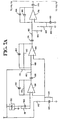
- FIG. 5 shows the transmitter circuit of the present invention.
- the voltage supply circuit (not shown) provides both positive and negative voltages to the transmitter circuit. As indicated above, the power is obtained from the associated electronic device and processed minimally to provide the required voltage levels for the transceiver.
- the transmitter circuit shown in Figure 5 in schematic form comprises the VSCEL laser 76, a ceramic resonator circuit, a transmitter encoder 80 which in the embodiment shown is a gate array logic processing circuit (GAL) which contains and executes logic equations for generating the pulses to be transmitted and a constant current source for driving laser 76.
- GAL gate array logic processing circuit
- the ceramic resonator circuit includes an inverter 84, a ceramic resonator 86, resistors 88 and 90 and capacitors 92 and 94.
- the ceramic resonator circuit produces an 800 kHz square wave clock signal at the output of inverter 84. The rising edge of this clock signal advances (clocks) the logic in the transmitter encoder 80.
- the encoder 80 generates an output signal (shown as a "fiber" signal in Figure 5), which causes light pulses to be transmitted from laser 76.
- an output signal shown as a "fiber" signal in Figure 5
- the electrical data signal which is to be transmitted from the electronic device is low, a 2.5 microsecond light pulse is transmitted every 13.5 microseconds.
- the transmit signal is high, two 2.5 microsecond pulses are transmitted every 28.75 microseconds.
- the equations present in GAL 80 to generate these pulses are shown in Figure 6.
- the transmit signal is applied to the encoder 80 by means of a circuit which includes a resistor 96, a resistor 98, FET 100 and resistor 102.
- the signal to the encoder 80 is an inverted version of the electrical data signal.
- FET 100 produces the transition from the data signal voltage levels to the logic voltage levels used in the encoder.
- the constant current source for the laser 76 drives the laser when the "fiber" signal from encoder 80 is high.
- the current is regulated, in the embodiment shown, between 11.5 milliamps to 13.5 milliamps over the selected temperature range.
- An approximate 1.2 volt reference is provided by operational amplifier 103 (pins 1,2 and 3)
- Operational amplifier (op-amp) 104 pins 5, 6 and 7) is connected as a follower.
- the negative feedback path forces the voltage at pin 6 to follow the voltage at pin 5.
- the voltage on pin 5 is the buffered output of the voltage regulator less one Schottky diode drop, as determined by diode 106 and resistor 108. This diode drop compensates for the diode drop of peak detector diode 110 and resistor 112.
- the source of the feedback path of the op-amp follower is a peak detection circuit for the voltage across resistor 114.
- the output of the op-amp 104 thus remains at a fairly constant DC voltage, even though FET 113 is being turned on and off to generate the optical pulses.
- the peak detector will have little ripple, which results in the output of the op-amp 104 remaining constant.
- the op-amp will drive transistor 118 into its active region the right amount of time to maintain a constant peak voltage across resistor 114, such that the peak voltage is equal to the voltage regulator reference voltage from op-amp 103, approximately 1.2 volts.
- the collector emitter voltage across transistor 118 will vary so as to keep the current flow through the laser constant whenever FET 113 is on.
- Resistor 120 in series with the gate of FET 113 will limit the current spike that could flow through transistor 118 when the FET is first turned on, while resistor 122 limits the transistor 118 base current when the transceiver is initially powering up.
- Capacitor 124 dampens the op-amp ringing that may occur when the FET 113 is initially turned on.
- the output of laser 76 is a series of optical pulses, such as shown in Figure 3. These optical pulses are then transmitted over the fiber-optic cable, of selected length, depending upon the application, to the transceiver at the other end of the line. The received optical pulses are applied to a receiver portion of the transceiver.
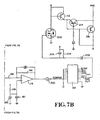
- the receiver portion of the transceiver is shown in Figure 7. Necessary power for the receiver is supplied by the voltage supply circuit which obtains its power from the associated electronic device to which it is connected, just like the transceiver at the transmitting end.
- the receiver circuit includes a pin photodiode 130, four op-amp stages, a GAL receiver decoder 132, which is similar to GAL 80 in the transmitter section and which converts the received optical pulses back to the original data signal form and a level shifting circuit to generate the data signal from GAL 132.
- GAL 132 in the embodiment shown is a gate array logic processing circuit which contains and executes the logic equations for decoding the received pulses into the original data signal.
- the four op-amp stages convert the optical pulses received from the fiber-optic cable into digital pulses which have enough resolution that single pulses can be readily distinguished from double pulses. As indicated above, a single received optical pulse will result in the reconstructed data signal being low, while a double optical pulse will result in the data signal being high.
- the first op-amp 138 determines the receiver sensitivity level. It operates as a transimpedance amplifier, converting a current signal into a voltage signal.
- the first stage op-amp maximizes the signal-to-noise ratio (SNR) for a given optical receiver level. This is accomplished by choosing the largest possible value for feedback resistor 140, since signal strength is directly proportional to the value of resistor 140, while the noise is directly proportional to the square root of resistor 140.
- SNR signal-to-noise ratio
- the maximum value of resistor 140 is determined by the minimum allowable bandwidth and the minimum value of capacitor 142 necessary to maintain stability of op-amp 138.
- a practical minimum value for capacitor 142 is 1 pF, while the minimum allowable bandwidth is determined by the digital pulse resolution required at the output of the last op-amp stage, which in this particular case is approximately 160 kHz.
- the minimum value of 1 pF for capacitor 142 and a minimum band width of 160 kHz establishes the value of the feedback resistor to be 1 MOhm.
- resistor 151 and capacitor 153 basically have no operational effect on the received signal, and the pin diode 130 is reverse-biased at approximately -3 volts. This reverse bias is accomplished with a supply voltage of +5 volts and a voltage divider formed by resistors 142, 144 and capacitor 146.
- This circuit is connected to the positive input of op-amp 138.
- the output of op-amp 138 when there is no received optical pulses, will be approximately 2 volts, less the DC voltage drop of the pin diode "dark" current (when no light is being received) through the 1 MOhm feedback resistor 140.
- pin diode 130 When an optical pulse (2.5 microseconds in the embodiment shown) is received, pin diode 130 produces 2.5 microseconds of current.
- the magnitude of the current pulse from the pin photodiode is based on the power level of the optical pulse and the responsivity of the pin photodiode.
- the gain of the op-amp 138 is approximately 10. At this gain level, a capacitor current divider exists between the feedback capacitor 142 and the parasitic capacitance of the op-amp input and pin photodiode. Approximately 1/2 to 3/4 of the pin diode current then actually flows through the feedback resistor 140.
- the first stage op-amp and associated circuitry is susceptible to noise, and accordingly is enclosed in an EMI-grounded shell, which shields the two high impedance nodes from radiated noise from the voltage supply circuit or the logic circuitry.
- the voltage supply for the first and second op-amps is filtered. The filtering removes unwanted noise generated by the supply voltage switching frequencies.
- the first stage op-amp It is important in order to accommodate a large, dynamic range of optical power levels that the first stage op-amp not be allowed to saturate. If op-amp 138 were driven into saturation, the width of the digital pulse of the resulting electrical signal would be so large that it would be impossible to make a correct distinction between single and double pulses.
- the op-amp 138 is kept from saturation by the 20 MOhm resistor 151 which is located between pin photodiode 130 and the first stage op-amp 138. Once the average pin photodiode current exceeds 150 nanoamperes, the pin photodiode will no longer be reverse biased. At this point, the pin photodiode is operating in the photovoltaic mode. Removing the reverse bias from the pin diode during high levels of optical power will also protect the pin diode from damage.
- capacitor 153 Since the peak positive voltage at the pin diode anode cannot exceed the forward voltage diode drop of around 0.7 volts above the +5 volt supply, the peak current flowing through resistor 151 is limited to 185 nanoamperes. This guarantees that the first stage op-amp will not go into saturation. Thus, for high optical power signals, the pin diode is maintained in the photovoltaic mode.
- the value of capacitor 153 is chosen so that there is only a minimal difference in the magnitude of current pulses that flow through feedback resistor 140. Capacitor 153 has a value such that there is only a small difference in the magnitude of the current pulses between when the pin diode is just barely reverse-biased (photoconductive mode) and just barely forward-biased (photovoltaic mode). Hence, there will not be large variances in the magnitude of the current pulses where the pin diode alternates rapidly between the photovoltaic and photoconductive modes due to slight variations in duty cycle.
- the first op-amp is decoupled from the second stage op-amp 156 by a capacitor 158.
- This capacitor 158 removes any DC signal which may be present in the op-amp output signal due to the photodiode "dark" current or first stage op-amp offsets.
- the primary purpose of op-amp 156 is to provide a large gain without introducing any significant levels of noise into the resulting signal.
- Op-amp 156 is configured as an inverting summing amplifier. Nominally, the AC signal gain is determined by feedback resistor 160 divided by the source resistor 162. The gain is limited, however, by the gain band width product (GBW) of the op-amp, which depends upon the characteristics of the particular op-amp selected.
- GW gain band width product
- Feedback capacitor 164 with feedback resistor 160 provides a low pass filter with a corner frequency of around 160 kHz.
- Resistor 168 in series with the negative input of the op-amp limits the power consumption of the first and second stage op-amps for high levels of optical power.
- op-amp 156 Applied to the negative input of op-amp 156 is the output of a unity buffer amplifier which is actually internal of the op-amp. The output of the op-amp is adjusted such that the current into or out of the negative input of the op-amp 156 is maintained at zero. However, if the op-amp goes into saturation, the negative input could "sink" a significant amount of current. Resistor 168 limits this current. Resistor 170 causes a DC signal to be summed with the input signal. Therefore, the output of the second op-amp when no optical pulses are being received is approximately 1.4 volts.
- the output of the second stage op-amp will be at saturation.
- the DC level shifting introduced by resistor 170 causes the "window" of the first stage output signal to be adjusted downwardly. This DC adjustment keeps this "window” away from the upper portion of the signal where an undamped response of the first stage could be mistaken for a received optical pulse.
- the window is kept away from the lower portion of the signal as well, where the magnitude of a second 2.5 microsecond pulse is not as strong and could be missed.
- the second op-amp stage is decoupled from the third stage by capacitor 174. This eliminates the DC current that was summed into the second op-amp stage, as well as any offset voltages and currents.
- the third op-amp 176 and fourth op-amp 178 in the embodiment shown are part of a dual op-amp.
- the purpose of the third stage op-amp 176 is to provide a gain of about 40 and to clamp the output signal at approximately +0.7 volts.
- the third op-amp 176 is configured as an inverted summing amplifier.
- the input signal gain is determined by a "feedback" resistance divided by a source resistor 182. Since there is no feedback resistor per se , the feedback resistance is determined by clamping diodes 184 and 186.
- the feedback resistance will be large, while for strong signals, the feedback resistance will be small.
- the gain of the third stage is also limited by the GBW of the op-amp.
- the output of the third stage will be fairly constant and the peak-to-peak voltage will remain somewhat less than 1.4 volts.
- the output signal will be centered about the DC bias (approximately 2 volts) of the op-amp, which is provided by the divider comprising resistor 188, resistor 190 and capacitor 192 connected to the op-amp.
- Resistor 194 causes a DC signal to be summed with the input signal.
- the output of the third op-amp stage when there are no optical pulses being received will be slightly greater than 2 volts.
- this addition of a DC level shifts the "window" for the third stage gain.
- this window shifts positive to be more centered about the peak-to-peak signal. This centering function causes the signal-to-noise ratio to be consistent when the second stage output is either at its high or low point.
- the fourth stage op-amp 178 converts the input signal into a digital signal.
- the fourth stage 178 is decoupled from the third stage by capacitor 179. This is accomplished through an inverting op-amp configuration, using a feedback resistor 196 and a source resistor 198.
- the output of the fourth-stage op-amp saturates for positive output and is clamped just above ground for a low or negative output.
- a DC bias point of approximately .7 volts is derived from diode 183, resistor 185 and capacitor 187.
- the output of the op-amp 178 is applied to a Schmitt trigger buffer 200 before being fed into the receiver decoder 132.
- the output of the Schmitt trigger goes low (pulses) in response to optical pulses being received by the pin diode.
- the delay between the receipt of the received optical signal at the input to the first op-amp and the output to the Schmitt trigger will be typically around 5 microseconds.
- the width of the pulses from the Schmitt trigger may also vary slightly, due to strength of the fiber-optic signal, temperature range variations, etc.
- the corresponding width of the output signal from the Schmitt trigger may be anywhere from 3.7-9 microseconds.
- the Schmitt trigger signal may be two narrow pulses or one long pulse.
- the width of the pulse can vary between 12.1-15.6 microseconds in the embodiment shown.
- the pulses are at least 4.2 microseconds wide and the second pulse begins not more than 8.7 microseconds from the rising edge of the first pulse.
- the receiver decoder 132 analyzes the input pulses from the Schmitt trigger circuit and generates the reconstructed digital signal. When only a single pulse is recognized, the decoder drives or maintains the receive digital signal low. When double pulses are recognized, the decoder drives or maintains the receive data signal high. Due to the ceramic resonator clocking the transmitter, the optical pulse widths received by the receiving transducer are very consistent, around 2.5 microseconds. The other timing for the optical pulses is quite consistent as well.
- the receiver decoder logic clock rate is 1.25 microseconds, so that the decision point in the embodiment shown between single and double pulses can be anywhere between 10-11.25 microseconds. After 10 microseconds, the single optical pulse would no longer be present. For the double pulse, after 11.25 microseconds, either the falling edge of both pulses would have occurred, or the second pulse would still be present.
- the decoder uses a three-bit counter to help count to 10 microseconds. It also uses two registers to count the number of pulses that have been received within the 10-microsecond span.
- Figure 8 shows the set of logic equations used in receiver decoder 132 to decode the received optical pulses into the original transmit signal.
- the actual data signal is generated by a level shifting transistor circuit. Diode 202, resistor 204 and capacitor 206 slightly delays the turning on of FET 208. This is done to balance the pulse widths of the high and low data signals. Otherwise, the pulse widths may be slightly distorted due to the FET used.
- FET 208 When the received signal from the decoder 132 goes high, FET 208 will turn on, after the slight delay. When the receive signal from the encoder goes low, FET 208 will be driven off.
- the positive and negative reference voltages are provided by the transducer voltage supply.
- the output signal transistor 212 will turn on when the base current flows due to FET 208 turning on.
- transistor 214 turns on due to transistor 212 turning on.
- the receive signal switches to a low level whenever transistor 212 turns off, which turns transistor 214 off and turns transistor 216 on.
- the resulting signal is a reconstruction of the original data transmit signal.
- a fiber-optic transceiver which because of a particular optical pulse arrangement representing the digital data signal and a particular hardware implementation thereof provides a transceiver which meets the eye safety standards, yet has sufficient power to transmit a fiber-optic signal over a considerable length of fiber-optic cable, depending to some extent upon the wave length of the optical transmitter.
Landscapes
- Physics & Mathematics (AREA)
- Electromagnetism (AREA)
- Engineering & Computer Science (AREA)
- Computer Networks & Wireless Communication (AREA)
- Signal Processing (AREA)
- Optical Communication System (AREA)
- Dc Digital Transmission (AREA)
- Communication Cables (AREA)
- Auxiliary Devices For And Details Of Packaging Control (AREA)
- Surgical Instruments (AREA)
Claims (16)
- Un émetteur et récepteur par fibre optique (10 ; 12) pour communication de données comprenant :des moyens (20) pour recevoir, à partir d'un dispositif terminal, un signal de données numériques présentant des états hauts et des états bas ;des moyens (20) pour former une série d'impulsions optiques à partir du signal de données, où une première disposition d'impulsions optiques représente un bord montant du signal de données et une seconde disposition d'impulsions optiques représente un bord descendant du signal de données, les première et seconde dispositions d'impulsions, respectivement, se produisant de manière répétée à des temps présélectionnés pendant lesdits états hauts et bas si les états hauts et bas dépassent une durée présélectionnée ;des moyens (22) pour émettre ladite série d'impulsions optiques le long d'un câble à fibre optique ;des moyens (53, 55) pour recevoir une série émise d'impulsions optiques en provenance d'un câble à fibre optique et pour reconnaître de première et seconde dispositions d'impulsions dans la série d'impulsions optiques et reconstruire à partir de là un signal de données numériques présentant des états hauts et bas, le signal de données numériques ainsi reconstruit étant sensiblement une copie du signal de données numériques à partir duquel a été formée une série d'impulsions optiques ; etdes moyens (55) pour fournir au dispositif terminal ledit signal de données numériques ainsi reconstruit,caractérisé en ce que la première disposition d'impulsions optiques est une impulsion double et la seconde disposition d'impulsions optiques est une impulsion unique.
- Un appareil selon la revendication 1, dans lequel le temps entre les bords montant et descendant du signal de données numériques et les première et seconde dispositions d'impulsions résultantes est approximativement d'un intervalle d'un bit du signal de données numériques.
- Un appareil selon la revendication 1, dans lequel la première disposition d'impulsions a une énergie moyenne approximativement égale à la moyenne de la seconde disposition d'impulsions.
- Un appareil selon l'une quelconque des revendications précédentes, dans lequel le temps présélectionné pour la première disposition d'impulsions est approximativement d'un intervalle de 1/2 bit et le temps présélectionné pour la seconde disposition d'impulsions est approximativement d'un intervalle d'un bit.
- Un appareil selon l'une quelconque des revendications précédentes, dans lequel l'énergie électrique de l'appareil est obtenue à partir du dispositif terminal électronique.
- Un appareil selon l'une quelconque des revendications précédentes, dans lequel la série d'impulsions optiques a un cycle opératoire qui est inférieur à 30 %.
- Un appareil selon la revendication 6, dans lequel la série émise d'impulsions optiques a un niveau de puissance qui ne présente pratiquement aucun danger pour les yeux de l'utilisateur.
- Un appareil selon l'une quelconque des revendications précédentes, comprenant des moyens pour fournir un secouage à la main pour le dispositif terminal.
- Un appareil selon l'une quelconque des revendications précédentes, dans lequel les moyens de formation comprennent un petit laser de faible puissance et un récepteur-codeur pour produire des signaux de commande pour le laser à partir du signal de données numériques.
- Un appareil de la revendication 9, dans lequel le laser est un laser VCSEL et les moyens de commande du récepteur-codeur comprennent des moyens à logique numérique et un oscillateur d'horloge pour commander lesdits moyens à logique numérique.
- Un appareil selon l'une quelconque des revendications précédentes, dans lequel les moyens de formation comprennent une DEL ainsi que des moyens pour produire des signaux de commande pour la DEL à partir du signal de données numériques.
- Un appareil selon l'une quelconque des revendications précédentes, dans lequel les moyens de formation sont capables d'utiliser le signal de données numériques directement issu de la borne de données, sans une quelconque modification de son format ou d'autres caractéristiques.
- Un appareil selon l'une quelconque des revendications précédentes, dans lequel les moyens de réception comprennent un photodiode PIN, une pluralité d'étages amplificateurs, un récepteur-décodeur et un dispositif de décalage de niveau pour produire un signal de données numériques reconstruit.
- Un appareil selon la revendication 13, comprenant quatre étages amplificateurs, où le premier étage amplificateur maximise le rapport signal sur bruit pour un niveau donné du récepteur optique, où les seconds et troisième étages fournissent une amplification desdites impulsions numériques et où le quatrième étage convertit en un signal numérique le signal vers le récepteur.
- Un appareil selon la revendication 13, dans lequel les moyens récepteurs sont couplés en courant alternatif, et où le récepteur-décodeur comprend des moyens à logique numérique et un oscillateur d'horloge pour commander les moyens à logique numérique.
- Un procédé de communication de données au moyen d'un câble à fibre optique, le procédé comprenant les étapes consistant à :recevoir, à partir d'un dispositif terminal, un signal de données numériques présentant des états hauts et des états bas ;former une série d'impulsions optiques à partir du signal de données, où une première disposition d'impulsions optiques représente un bord montant du signal de données et une seconde disposition d'impulsions optiques représente un bord descendant du signal de données, les première et seconde dispositions d'impulsions, respectivement se produisant de manière répétée à des temps présélectionnés pendant les états hauts et bas si les états hauts et bas dépassent une durée présélectionnée ;émettre ladite série d'impulsions optiques le long d'un câble à fibre optique ;recevoir une série émise d'impulsions optiques en provenance d'un câble à fibre optique, reconnaître de première et seconde dispositions d'impulsions dans la série d'impulsions optiques et reconstruire à partir de là un signal de données numériques présentant des états hauts et bas, le signal de données numériques ainsi reconstruit étant sensiblement une copie du signal de données numériques à partir duquel a été formée une série d'impulsions optiques ; etfournir au dispositif terminal ledit signal de données numériques ainsi reconstruit,caractérisé en ce que la première disposition d'impulsions optiques est une impulsion double et la seconde disposition d'impulsions optiques est une impulsion unique.
Applications Claiming Priority (2)
| Application Number | Priority Date | Filing Date | Title |
|---|---|---|---|
| US08/953,170 US6188494B1 (en) | 1997-10-17 | 1997-10-17 | Fiber-optic transceiver for long distance data communications |
| US953170 | 1997-10-17 |
Publications (3)
| Publication Number | Publication Date |
|---|---|
| EP0917309A2 EP0917309A2 (fr) | 1999-05-19 |
| EP0917309A3 EP0917309A3 (fr) | 2003-11-12 |
| EP0917309B1 true EP0917309B1 (fr) | 2005-09-21 |
Family
ID=25493672
Family Applications (1)
| Application Number | Title | Priority Date | Filing Date |
|---|---|---|---|
| EP98308369A Expired - Lifetime EP0917309B1 (fr) | 1997-10-17 | 1998-10-14 | Emetteur et récepteur par fibre optique pour communications de données à longue distance |
Country Status (7)
| Country | Link |
|---|---|
| US (1) | US6188494B1 (fr) |
| EP (1) | EP0917309B1 (fr) |
| CN (1) | CN1265565C (fr) |
| AT (1) | ATE305187T1 (fr) |
| BR (1) | BR9803929A (fr) |
| DE (1) | DE69831636T2 (fr) |
| ES (1) | ES2247663T3 (fr) |
Families Citing this family (32)
| Publication number | Priority date | Publication date | Assignee | Title |
|---|---|---|---|---|
| US20030042571A1 (en) | 1997-10-23 | 2003-03-06 | Baoxing Chen | Chip-scale coils and isolators based thereon |
| JP2000049712A (ja) * | 1998-05-28 | 2000-02-18 | Sharp Corp | ディジタル光通信装置およびその方法 |
| US6590687B1 (en) * | 1999-03-11 | 2003-07-08 | El Paso Natural Gas | Low power optically coupled serial data link |
| US6920289B2 (en) * | 2001-02-01 | 2005-07-19 | International Business Machines Corporation | System and method for remote optical digital networking of computing devices |
| US7605649B2 (en) * | 2001-03-13 | 2009-10-20 | Marvell World Trade Ltd. | Nested transimpedance amplifier |
| US7551024B2 (en) * | 2001-03-13 | 2009-06-23 | Marvell World Trade Ltd. | Nested transimpedance amplifier |
| US7276965B1 (en) | 2001-03-13 | 2007-10-02 | Marvell International Ltd. | Nested transimpedance amplifier |
| US20030157891A1 (en) * | 2002-02-15 | 2003-08-21 | Masahiro Maki | Method and apparatus for inspecting cable set and method for selecting cable set in transmission line, and communications system |
| US7342884B2 (en) * | 2002-03-13 | 2008-03-11 | Harmonic, Inc. | Method and apparatus for one directional communications in bidirectional communications channel |
| DE10262239B4 (de) | 2002-09-18 | 2011-04-28 | Infineon Technologies Ag | Digitales Signalübertragungsverfahren |
| US7088518B2 (en) * | 2002-12-03 | 2006-08-08 | Finisar Corporation | Bidirectional optical device |
| US7075329B2 (en) * | 2003-04-30 | 2006-07-11 | Analog Devices, Inc. | Signal isolators using micro-transformers |
| US7558014B1 (en) | 2004-06-24 | 2009-07-07 | Marvell International Ltd. | Programmable high pass amplifier for perpendicular recording systems |
| CN100388591C (zh) * | 2004-12-24 | 2008-05-14 | 许继集团有限公司 | 一种继电保护信号传输中的大码距分组码编解码方法 |
| JP4550712B2 (ja) * | 2005-10-17 | 2010-09-22 | ルネサスエレクトロニクス株式会社 | 受光回路 |
| US8139948B2 (en) * | 2006-06-12 | 2012-03-20 | Acist Medical Systems, Inc. | Process and system for providing electrical energy to a shielded medical imaging suite |
| KR101430168B1 (ko) * | 2008-01-09 | 2014-08-13 | 삼성전자주식회사 | 3단계 신호를 송수신하는 광 송수신 장치 |
| JP5315839B2 (ja) * | 2008-08-01 | 2013-10-16 | 日本電気株式会社 | 光通信装置及び光出力制御方法及び光通信システム及びプログラム |
| US20100124272A1 (en) * | 2008-11-19 | 2010-05-20 | Gene Fein | Coded pulse data transmission using a look-up table |
| EP2399350B1 (fr) * | 2009-02-23 | 2017-10-18 | Hewlett-Packard Enterprise Development LP | Circuit récepteur à détecteur optique à impédance dynamique |
| CN101800597B (zh) * | 2010-02-04 | 2013-07-10 | 深圳市金宏威技术股份有限公司 | 一种防止光纤接口抖动的方法及系统 |
| GB2506383A (en) * | 2012-09-27 | 2014-04-02 | Isis Innovation | Apparatus and method for data communication that uses optical concentration devices |
| US9065544B2 (en) * | 2012-09-28 | 2015-06-23 | Osram Sylvania Inc. | Pulse-based binary communication |
| WO2014063728A1 (fr) * | 2012-10-24 | 2014-05-01 | Kongsberg Defence & Aerospace As | Commande d'armes par fibre optique de sécurité |
| US9293997B2 (en) | 2013-03-14 | 2016-03-22 | Analog Devices Global | Isolated error amplifier for isolated power supplies |
| US9660848B2 (en) | 2014-09-15 | 2017-05-23 | Analog Devices Global | Methods and structures to generate on/off keyed carrier signals for signal isolators |
| US10270630B2 (en) | 2014-09-15 | 2019-04-23 | Analog Devices, Inc. | Demodulation of on-off-key modulated signals in signal isolator systems |
| US10536309B2 (en) | 2014-09-15 | 2020-01-14 | Analog Devices, Inc. | Demodulation of on-off-key modulated signals in signal isolator systems |
| US9998301B2 (en) | 2014-11-03 | 2018-06-12 | Analog Devices, Inc. | Signal isolator system with protection for common mode transients |
| US10659168B2 (en) * | 2016-08-23 | 2020-05-19 | Schweitzer Engineering Laboratories, Inc. | Low-power fiber optic transceiver |
| US11309975B2 (en) | 2020-02-10 | 2022-04-19 | Schweitzer Engineering Laboratories, Inc. | Fiber-optically powered antenna |
| US12334977B2 (en) | 2022-12-19 | 2025-06-17 | Schweitzer Engineering Laboratories, Inc. | Fiber optic signal monitoring |
Family Cites Families (7)
| Publication number | Priority date | Publication date | Assignee | Title |
|---|---|---|---|---|
| FR2511824A1 (fr) * | 1981-08-21 | 1983-02-25 | Thomson Csf | Systeme emetteur-recepteur de transmission numerique par voie optique et a debit variable |
| US4584719A (en) * | 1984-08-24 | 1986-04-22 | System Development Corp. | Fiber optic workstation datalink interface |
| US4713841A (en) * | 1985-06-03 | 1987-12-15 | Itt Electro Optical Products, A Division Of Itt Corporation | Synchronous, asynchronous, data rate transparent fiber optic communications link |
| DE3524871A1 (de) * | 1985-07-12 | 1987-01-22 | Licentia Gmbh | Verfahren zur optischen rbertragung binaerer signale und anordnung zur durchfuehrung des verfahrens |
| US5559053A (en) * | 1994-04-14 | 1996-09-24 | Lucent Technologies Inc. | Vertical cavity semiconductor laser |
| US5905758A (en) * | 1996-04-24 | 1999-05-18 | Schweitzer Engineering Laboratories | Fiber-optic transceiver for combined serial data and time code communication |
| US5914976A (en) * | 1997-01-08 | 1999-06-22 | W. L. Gore & Associates, Inc. | VCSEL-based multi-wavelength transmitter and receiver modules for serial and parallel optical links |
-
1997
- 1997-10-17 US US08/953,170 patent/US6188494B1/en not_active Expired - Lifetime
-
1998
- 1998-10-14 ES ES98308369T patent/ES2247663T3/es not_active Expired - Lifetime
- 1998-10-14 EP EP98308369A patent/EP0917309B1/fr not_active Expired - Lifetime
- 1998-10-14 DE DE69831636T patent/DE69831636T2/de not_active Expired - Fee Related
- 1998-10-14 AT AT98308369T patent/ATE305187T1/de not_active IP Right Cessation
- 1998-10-16 CN CNB981209696A patent/CN1265565C/zh not_active Expired - Fee Related
- 1998-10-16 BR BR9803929-6A patent/BR9803929A/pt not_active IP Right Cessation
Also Published As
| Publication number | Publication date |
|---|---|
| BR9803929A (pt) | 1999-12-21 |
| EP0917309A3 (fr) | 2003-11-12 |
| EP0917309A2 (fr) | 1999-05-19 |
| US6188494B1 (en) | 2001-02-13 |
| ES2247663T3 (es) | 2006-03-01 |
| CN1223507A (zh) | 1999-07-21 |
| CN1265565C (zh) | 2006-07-19 |
| ATE305187T1 (de) | 2005-10-15 |
| DE69831636T2 (de) | 2006-06-14 |
| DE69831636D1 (de) | 2005-10-27 |
Similar Documents
| Publication | Publication Date | Title |
|---|---|---|
| EP0917309B1 (fr) | Emetteur et récepteur par fibre optique pour communications de données à longue distance | |
| US6724993B2 (en) | Optical transmitter-receiver | |
| US6075634A (en) | Gigabit data rate extended range fiber optic communication system and transponder therefor | |
| US4471494A (en) | Optical transmission system for high frequency digital signals | |
| US5510919A (en) | Optical system for transmitting a multilevel signal | |
| US4620321A (en) | Optical fibre receiver | |
| US4236256A (en) | Asynchronous data receiver | |
| US20020027689A1 (en) | Fiber optic transceiver employing front end level control | |
| US4481676A (en) | Transmitter-receiver system for variable-rate digital data transmission via optical-fiber links | |
| US5214526A (en) | Pulse modulated infrared data communications link | |
| JPH0131741B2 (fr) | ||
| US5255111A (en) | Full-duplex optical transmission system | |
| US6535308B1 (en) | Method and apparatus for converting electrical signals and optical signals for bidirectional communication over a single optical fiber | |
| EP0292117A1 (fr) | Circuit d'ajustement de seuil automatique pour transmission de données numérique | |
| CN110943781A (zh) | 一种单模光纤和多模光纤的模式转换设备 | |
| JP2536178B2 (ja) | 光送受信器 | |
| CN204990748U (zh) | 一种具有应急电源的智能交通防碰撞装置 | |
| CA1217818A (fr) | Systeme modulateur-demodulateur optique | |
| JP3607378B2 (ja) | 光送信装置および動作条件調整支援装置 | |
| TW202220399A (zh) | 收發裝置、終端裝置以及收發系統 | |
| JPH04123482A (ja) | 光伝送装置 | |
| JPS60169248A (ja) | 光フアイバ通信方式 | |
| JP2006060640A (ja) | 光受信回路およびその識別閾値制御方法 | |
| JPH08316520A (ja) | 光/電気変換回路 | |
| JPS6362429A (ja) | 送受信装置 |
Legal Events
| Date | Code | Title | Description |
|---|---|---|---|
| PUAI | Public reference made under article 153(3) epc to a published international application that has entered the european phase |
Free format text: ORIGINAL CODE: 0009012 |
|
| AK | Designated contracting states |
Kind code of ref document: A2 Designated state(s): AT BE CH CY DE DK ES FI FR GB GR IE IT LI LU MC NL PT SE |
|
| AX | Request for extension of the european patent |
Free format text: AL;LT;LV;MK;RO;SI |
|
| PUAL | Search report despatched |
Free format text: ORIGINAL CODE: 0009013 |
|
| AK | Designated contracting states |
Kind code of ref document: A3 Designated state(s): AT BE CH CY DE DK ES FI FR GB GR IE IT LI LU MC NL PT SE |
|
| AX | Request for extension of the european patent |
Extension state: AL LT LV MK RO SI |
|
| 17P | Request for examination filed |
Effective date: 20040428 |
|
| AKX | Designation fees paid |
Designated state(s): AT BE CH CY DE DK ES FI FR GB GR IE IT LI LU MC NL PT SE |
|
| 17Q | First examination report despatched |
Effective date: 20041112 |
|
| GRAP | Despatch of communication of intention to grant a patent |
Free format text: ORIGINAL CODE: EPIDOSNIGR1 |
|
| GRAS | Grant fee paid |
Free format text: ORIGINAL CODE: EPIDOSNIGR3 |
|
| GRAA | (expected) grant |
Free format text: ORIGINAL CODE: 0009210 |
|
| AK | Designated contracting states |
Kind code of ref document: B1 Designated state(s): AT BE CH CY DE DK ES FI FR GB GR IE IT LI LU MC NL PT SE |
|
| PG25 | Lapsed in a contracting state [announced via postgrant information from national office to epo] |
Ref country code: NL Free format text: LAPSE BECAUSE OF FAILURE TO SUBMIT A TRANSLATION OF THE DESCRIPTION OR TO PAY THE FEE WITHIN THE PRESCRIBED TIME-LIMIT Effective date: 20050921 Ref country code: FI Free format text: LAPSE BECAUSE OF FAILURE TO SUBMIT A TRANSLATION OF THE DESCRIPTION OR TO PAY THE FEE WITHIN THE PRESCRIBED TIME-LIMIT Effective date: 20050921 Ref country code: BE Free format text: LAPSE BECAUSE OF FAILURE TO SUBMIT A TRANSLATION OF THE DESCRIPTION OR TO PAY THE FEE WITHIN THE PRESCRIBED TIME-LIMIT Effective date: 20050921 Ref country code: AT Free format text: LAPSE BECAUSE OF FAILURE TO SUBMIT A TRANSLATION OF THE DESCRIPTION OR TO PAY THE FEE WITHIN THE PRESCRIBED TIME-LIMIT Effective date: 20050921 |
|
| REG | Reference to a national code |
Ref country code: GB Ref legal event code: FG4D |
|
| REG | Reference to a national code |
Ref country code: CH Ref legal event code: EP |
|
| PG25 | Lapsed in a contracting state [announced via postgrant information from national office to epo] |
Ref country code: IE Free format text: LAPSE BECAUSE OF NON-PAYMENT OF DUE FEES Effective date: 20051014 Ref country code: CY Free format text: LAPSE BECAUSE OF FAILURE TO SUBMIT A TRANSLATION OF THE DESCRIPTION OR TO PAY THE FEE WITHIN THE PRESCRIBED TIME-LIMIT Effective date: 20051014 |
|
| REG | Reference to a national code |
Ref country code: IE Ref legal event code: FG4D |
|
| REF | Corresponds to: |
Ref document number: 69831636 Country of ref document: DE Date of ref document: 20051027 Kind code of ref document: P |
|
| PG25 | Lapsed in a contracting state [announced via postgrant information from national office to epo] |
Ref country code: MC Free format text: LAPSE BECAUSE OF NON-PAYMENT OF DUE FEES Effective date: 20051031 |
|
| REG | Reference to a national code |
Ref country code: CH Ref legal event code: NV Representative=s name: E. BLUM & CO. PATENTANWAELTE |
|
| PG25 | Lapsed in a contracting state [announced via postgrant information from national office to epo] |
Ref country code: LU Free format text: LAPSE BECAUSE OF NON-PAYMENT OF DUE FEES Effective date: 20051121 |
|
| REG | Reference to a national code |
Ref country code: SE Ref legal event code: TRGR |
|
| PG25 | Lapsed in a contracting state [announced via postgrant information from national office to epo] |
Ref country code: GR Free format text: LAPSE BECAUSE OF FAILURE TO SUBMIT A TRANSLATION OF THE DESCRIPTION OR TO PAY THE FEE WITHIN THE PRESCRIBED TIME-LIMIT Effective date: 20051221 Ref country code: DK Free format text: LAPSE BECAUSE OF FAILURE TO SUBMIT A TRANSLATION OF THE DESCRIPTION OR TO PAY THE FEE WITHIN THE PRESCRIBED TIME-LIMIT Effective date: 20051221 |
|
| PG25 | Lapsed in a contracting state [announced via postgrant information from national office to epo] |
Ref country code: PT Free format text: LAPSE BECAUSE OF FAILURE TO SUBMIT A TRANSLATION OF THE DESCRIPTION OR TO PAY THE FEE WITHIN THE PRESCRIBED TIME-LIMIT Effective date: 20060221 |
|
| NLV1 | Nl: lapsed or annulled due to failure to fulfill the requirements of art. 29p and 29m of the patents act | ||
| REG | Reference to a national code |
Ref country code: ES Ref legal event code: FG2A Ref document number: 2247663 Country of ref document: ES Kind code of ref document: T3 |
|
| ET | Fr: translation filed | ||
| PLBE | No opposition filed within time limit |
Free format text: ORIGINAL CODE: 0009261 |
|
| STAA | Information on the status of an ep patent application or granted ep patent |
Free format text: STATUS: NO OPPOSITION FILED WITHIN TIME LIMIT |
|
| REG | Reference to a national code |
Ref country code: IE Ref legal event code: MM4A |
|
| 26N | No opposition filed |
Effective date: 20060622 |
|
| PGFP | Annual fee paid to national office [announced via postgrant information from national office to epo] |
Ref country code: GB Payment date: 20061002 Year of fee payment: 9 |
|
| PGFP | Annual fee paid to national office [announced via postgrant information from national office to epo] |
Ref country code: ES Payment date: 20061011 Year of fee payment: 9 Ref country code: CH Payment date: 20061011 Year of fee payment: 9 |
|
| PGFP | Annual fee paid to national office [announced via postgrant information from national office to epo] |
Ref country code: SE Payment date: 20061017 Year of fee payment: 9 |
|
| PGFP | Annual fee paid to national office [announced via postgrant information from national office to epo] |
Ref country code: IT Payment date: 20061031 Year of fee payment: 9 |
|
| PGFP | Annual fee paid to national office [announced via postgrant information from national office to epo] |
Ref country code: DE Payment date: 20061227 Year of fee payment: 9 |
|
| REG | Reference to a national code |
Ref country code: CH Ref legal event code: PFA Owner name: SCHWEITZER ENGINEERING LABORATORIES, INC. Free format text: SCHWEITZER ENGINEERING LABORATORIES, INC.#2350 NORTHEAST HOPKINS COURT#PULLMANN, WA 99163 (US) -TRANSFER TO- SCHWEITZER ENGINEERING LABORATORIES, INC.#2350 NORTHEAST HOPKINS COURT#PULLMANN, WA 99163 (US) |
|
| EUG | Se: european patent has lapsed | ||
| GBPC | Gb: european patent ceased through non-payment of renewal fee |
Effective date: 20071014 |
|
| REG | Reference to a national code |
Ref country code: CH Ref legal event code: PL |
|
| PG25 | Lapsed in a contracting state [announced via postgrant information from national office to epo] |
Ref country code: LI Free format text: LAPSE BECAUSE OF NON-PAYMENT OF DUE FEES Effective date: 20071031 Ref country code: DE Free format text: LAPSE BECAUSE OF NON-PAYMENT OF DUE FEES Effective date: 20080501 Ref country code: CH Free format text: LAPSE BECAUSE OF NON-PAYMENT OF DUE FEES Effective date: 20071031 |
|
| REG | Reference to a national code |
Ref country code: FR Ref legal event code: ST Effective date: 20080630 |
|
| PG25 | Lapsed in a contracting state [announced via postgrant information from national office to epo] |
Ref country code: SE Free format text: LAPSE BECAUSE OF NON-PAYMENT OF DUE FEES Effective date: 20071015 |
|
| PGFP | Annual fee paid to national office [announced via postgrant information from national office to epo] |
Ref country code: FR Payment date: 20061012 Year of fee payment: 9 |
|
| PG25 | Lapsed in a contracting state [announced via postgrant information from national office to epo] |
Ref country code: GB Free format text: LAPSE BECAUSE OF NON-PAYMENT OF DUE FEES Effective date: 20071014 |
|
| REG | Reference to a national code |
Ref country code: ES Ref legal event code: FD2A Effective date: 20071015 |
|
| PG25 | Lapsed in a contracting state [announced via postgrant information from national office to epo] |
Ref country code: FR Free format text: LAPSE BECAUSE OF NON-PAYMENT OF DUE FEES Effective date: 20071031 Ref country code: ES Free format text: LAPSE BECAUSE OF NON-PAYMENT OF DUE FEES Effective date: 20071015 |
|
| PG25 | Lapsed in a contracting state [announced via postgrant information from national office to epo] |
Ref country code: IT Free format text: LAPSE BECAUSE OF NON-PAYMENT OF DUE FEES Effective date: 20071014 |