EP0917778B1 - Procede et appareil de reception d'un signal dans un systeme de communication numerique a radiofrequence - Google Patents
Procede et appareil de reception d'un signal dans un systeme de communication numerique a radiofrequence Download PDFInfo
- Publication number
- EP0917778B1 EP0917778B1 EP97925661A EP97925661A EP0917778B1 EP 0917778 B1 EP0917778 B1 EP 0917778B1 EP 97925661 A EP97925661 A EP 97925661A EP 97925661 A EP97925661 A EP 97925661A EP 0917778 B1 EP0917778 B1 EP 0917778B1
- Authority
- EP
- European Patent Office
- Prior art keywords
- signal
- outputs
- output
- time
- received
- Prior art date
- Legal status (The legal status is an assumption and is not a legal conclusion. Google has not performed a legal analysis and makes no representation as to the accuracy of the status listed.)
- Expired - Lifetime
Links
- 238000000034 method Methods 0.000 title claims description 26
- 238000004891 communication Methods 0.000 title description 44
- 230000003111 delayed effect Effects 0.000 claims description 4
- 238000007476 Maximum Likelihood Methods 0.000 description 7
- 238000010586 diagram Methods 0.000 description 6
- 238000001228 spectrum Methods 0.000 description 5
- 230000001413 cellular effect Effects 0.000 description 4
- 230000001427 coherent effect Effects 0.000 description 4
- 238000011084 recovery Methods 0.000 description 4
- 239000011159 matrix material Substances 0.000 description 3
- 239000000737 potassium alginate Substances 0.000 description 3
- 230000008569 process Effects 0.000 description 3
- 238000012545 processing Methods 0.000 description 3
- 238000012937 correction Methods 0.000 description 2
- 230000010363 phase shift Effects 0.000 description 2
- 230000011664 signaling Effects 0.000 description 2
- 230000005540 biological transmission Effects 0.000 description 1
- 238000010276 construction Methods 0.000 description 1
- 238000001514 detection method Methods 0.000 description 1
- 238000001914 filtration Methods 0.000 description 1
- 230000003993 interaction Effects 0.000 description 1
- 238000012986 modification Methods 0.000 description 1
- 230000004048 modification Effects 0.000 description 1
- 239000013307 optical fiber Substances 0.000 description 1
- 230000004044 response Effects 0.000 description 1
- 230000007480 spreading Effects 0.000 description 1
Images

Classifications
-
- H—ELECTRICITY
- H04—ELECTRIC COMMUNICATION TECHNIQUE
- H04L—TRANSMISSION OF DIGITAL INFORMATION, e.g. TELEGRAPHIC COMMUNICATION
- H04L7/00—Arrangements for synchronising receiver with transmitter
-
- H—ELECTRICITY
- H04—ELECTRIC COMMUNICATION TECHNIQUE
- H04B—TRANSMISSION
- H04B1/00—Details of transmission systems, not covered by a single one of groups H04B3/00 - H04B13/00; Details of transmission systems not characterised by the medium used for transmission
- H04B1/69—Spread spectrum techniques
- H04B1/707—Spread spectrum techniques using direct sequence modulation
- H04B1/7073—Synchronisation aspects
- H04B1/7085—Synchronisation aspects using a code tracking loop, e.g. a delay-locked loop
-
- H—ELECTRICITY
- H04—ELECTRIC COMMUNICATION TECHNIQUE
- H04L—TRANSMISSION OF DIGITAL INFORMATION, e.g. TELEGRAPHIC COMMUNICATION
- H04L7/00—Arrangements for synchronising receiver with transmitter
- H04L7/02—Speed or phase control by the received code signals, the signals containing no special synchronisation information
- H04L7/033—Speed or phase control by the received code signals, the signals containing no special synchronisation information using the transitions of the received signal to control the phase of the synchronising-signal-generating means, e.g. using a phase-locked loop
- H04L7/0331—Speed or phase control by the received code signals, the signals containing no special synchronisation information using the transitions of the received signal to control the phase of the synchronising-signal-generating means, e.g. using a phase-locked loop with a digital phase-locked loop [PLL] processing binary samples, e.g. add/subtract logic for correction of receiver clock
Definitions
- This invention relates generally to wireless communication systems, and, more particularly, to a method and apparatus for receiving a signal in a digital radio frequency communication system.
- a base station having a controller and a plurality of transmitters and receivers communicates via an RF channel with a mobile station operating within an area served by the base station.
- RF radio frequency
- Transmitting a communication signal over an RF channel through a medium such as air causes a received communication signal to significantly differ from the originally transmitted communication signal.
- the transmitted communication signal may be altered by slowly-changing channel parameters such as channel gain, phase shift and time delay, and may further be corrupted by an amount of noise.
- a receiver particularly a non-coherent receiver, to maintain accurate timing during recovery of the communication signal.
- WO 96 22661 A discloses a method and apparatus for tracking the frequency and phase of signals in spread spectrum communication systems that makes more efficient use of available carrier frequency and phase information by utilizing a substantial portion or all of the energy occupying the frequency spectrum of a received carrier signal, including energy from communication signals intended for other system users.
- Multiple spread spectrum communication signals are input in parallel to data receivers where they are despread using preselected despreading codes at an adjustable phase angle and decoded over multiple orthogonal codes active within the communication system.
- Multiple decoded signals are then combined to form a single phase detection signal which is used by at least one tracking loop to track frequency and phase of the carrier signal for the received communication signals.
- the tracking loop generates a timing signal which is used to adjust the phase angle used during despreading.
- the communication signals are despread using appropriate PN codes and separated into in-phase (I) and quadrature channels (Q) where data symbols are processed by fast Hadamard transformers to generate corresponding data bits.
- the data is formed into pairwise products between the channels and summed over multiple or all active subscriber orthogonal codes. This sum indicates a degree to which the estimated phase differs from the actual phase of received communication signals and is used to adjust the phase of application for the PN codes.
- US 4,805,191 discloses that in a digital data receiver, it is desirable to use the equalized data for deriving time synchronization information.
- the invention of D2 purports to minimize timing contention between an equalizer operating at a T/2 rate and a timing recovery circuit which utilizes the output of the equalizer.
- An interpolator interpolates T1 and T2 data samples from the equalizer and provides data signals R and S equally spaced relative to the peak baud amplitude which can be easily processed by the timing recovery circuit.
- a method for receiving a signal comprising a plurality of received symbols associated with a plurality of transmitted symbols, as claimed in claim 1.
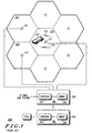
- FIG. 1 illustrates a wireless communication system 200 , such as a code division multiple access (CDMA) digital radiotelephone system.
- Base stations 210, 212 and 214 communicate with a mobile station 216 operating within an area 220 served by base station 212 . Areas 222 and 224 are served by base stations 214 and 210, respectively.
- Base stations 210, 212 and 214 are coupled to a base station controller 250, which includes, among other things, a processor 262 and a memory 264 , and which is in turn coupled to a mobile switching center 260, also including a processor 262 and a memory 264.
- a base station controller 250 which includes, among other things, a processor 262 and a memory 264 , and which is in turn coupled to a mobile switching center 260, also including a processor 262 and a memory 264.
- RF radio frequency
- Base-to-mobile station communications are said to occur on a forward-link channel, while mobile-to-base station communications are referred to as being on a reverse-link channel.
- a communication system using CDMA channelization is described in detail in TIA/EIA Interim Standard IS-95A, Mobile Station-Base Station Compatibility Standards for Dual-Mode Wideband Spread Spectrum Cellular Systems, Telecommunications Industry Association, Washington, D.C. July 1993 [IS-95A], and "TIA Telecommunications Systems Bulletin: Support for 14.4 kbps Data Rate and PCS Interaction for Wideband Spread Spectrum Cellular Systems", February 1996 [the Bulletin], both IS-95A and the Bulletin.
- communication signal 213 has been transmitted on an IS-95 forward-link channel such as a Paging Channel or a Traffic Channel by base station 212 to mobile station 216.
- Communication signal 215 has been transmitted via an IS-95 reverse-link channel such as an Access Channel or a Traffic Channel by mobile station 216 to base station 212 .
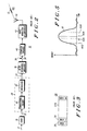
- FIG. 2 is a block diagram of a transmitter 10 , for use in a mobile station such as mobile station 216 , for generating communication signal 215.
- Encoder block 28 includes a convolutional encoder 30 and an interleaver 32 .
- transmit channel frame may be encoded by a rate 1/3 encoder using well-known algorithms such as convolutional encoding algorithms which facilitate subsequent decoding of the frames.
- Interleaver 32 operates to shuffle the contents of the frames using commonly-known techniques such as block interleaving techniques.
- each frame 34 of digitally coded and interleaved bits includes ninety-six groups of six coded bits, for a total of 576 bits.
- Each group of six coded bits represents an index 35 to one of sixty-four symbols such as Walsh codes.
- a Walsh code corresponds to a single row or column of a sixty-four-by-sixty-four Hadamard matrix, a square matrix of bits with a dimension that is a power of two.
- the bits comprising a Walsh code are referred to as Walsh chips.
- each of the ninety-six Walsh code indices 35 in frame 34 are input to an M-ary orthogonal modulator 36 , which is preferably a sixty-four-ary orthogonal modulator.
- M-ary orthogonal modulator 36 For each input Walsh code index 35, M-ary orthogonal modulator 36 generates at output 38 a corresponding sixty-four-bit Walsh code W 39.
- W 39 a series of ninety-six Walsh codes W 39 is generated for each frame 34 input to M-ary orthogonal modulator 36.
- Scrambler/spreader block 40 applies a pseudorandom noise (PN) sequence to the series of Walsh codes W 39 using well-known scrambling techniques.
- PN pseudorandom noise
- the scrambled series of Walsh codes W 39 is phase modulated using an offset quaternary phase-shift keying (OQPSK) modulation process or another modulation process, up-converted and transmitted as communication signal S(T) 12 from antenna 46 .
- OFPSK offset quaternary phase-shift keying
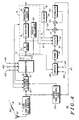
- FIG. 4 is a partial block diagram of an apparatus 60 within a base station such as base station 212 (shown in FIG. 1), for receiving communication signal R(T), originally transmitted by mobile station 216 as communication signal S(T) 12.
- Receiver 60 is preferably a RAKE receiver having a number of fingers, although only a single finger is shown.
- Receiver 60 may be coherent, non-coherent or quasi-coherent.
- Antenna 62 receives communication signal R(T) 18, which comprises a number of received frames.
- Front-end processing such as filtering, frequency down-converting and phase demodulation of communication signal R(T) 18 is performed by well-known methods and circuits at block 64.
- Searcher 300 attempts to lock onto received signal R(T) 18 at approximately the time of reception of R(T) 18 , looking for R(T) 18 at a plurality of time offsets.
- receiver 60 may also monitor R(T) 18 at a time offset slightly earlier than OT 400 , referred to as early offset E 402 , and at a time offset slightly later than OT 400, known as late offset L 404.
- Early offset E 402 and late offset 404 are preferably approximately one Walsh chip period apart.
- de-scrambler/de-spreader block 66 removes the PN code applied by scrambler block 44 (shown in FIG. 2) to the series of Walsh codes W 39 (also shown in FIG. 2).
- a received frame of received signal 18 includes ninety-six received symbols, or Walsh codes, which are each sixty-four bits long.
- the received Walsh codes have been altered during transmission by various channel parameters, however, and simply appear to receiver 60 to be received signal samples. Nevertheless, the received Walsh codes are referred to herein as received Walsh codes RW.
- each received Walsh code RW 68 after leaving de-scrambler/de-spreader 66 , is input to an orthogonal demodulator 70, such as a Fast Hadamard Transform (FHT).
- FHT 70 may be implemented using commercially available hardware as an array of adders or as a multiplexed adder, depending on its size.
- FHT 70 may be implemented utilizing a conventional digital signal processor (DSP) such as a Motorola DSP, part no. 56166 or an application specific integrated circuit (ASIC).
- DSP digital signal processor
- ASIC application specific integrated circuit
- FHT 70 Upon receiving a received Walsh code RW 68, FHT 70 generates a number of output signals 72. Outputs 72 associated with the received Walsh code RW 68 input to FHT 70 at early offset time E 402 are referred to as the set of early outputs, outputs 72 produced by FHT 70 in response to the received Walsh code 68 at on-time offset time OT 400 are referred to as the set of on-time outputs, and outputs 72 associated with late offset time L 404 are referred to as the set of late outputs.
- Each output signal 72 is generated by FHT 70 per Walsh code RW 68 .
- Each output signal 72 has an index which references one of the sixty-four possible Walsh codes w 39 generated by M-ary orthogonal modulator 36 (shown in FIG. 2).
- M-ary orthogonal modulator 36 shown in FIG. 2.
- each output signal 72 also has an associated complex number (not shown). Seven bits are preferably allocated to the real and imaginary portions, respectively, of the complex number, although fewer or more bits are possible. For simplicity, the index and the complex number will be referred to collectively as output signal 72.
- Each output signal 72 further has an associated energy value (not shown), commonly calculated by magnitude-squaring the complex number associated with output signal 72 .
- the energy value generally corresponds to a measure of confidence, or a likelihood, that output signal 72 indexes a Walsh code W 39 which corresponds to a received Walsh codes RW 68 input to FHT 70 .
- the energy value may have any suitable bit width, and may be, for example, fourteen bits wide.
- decoder block 76 Acting on the set of on-time outputs, decoder block 76, which may include a Maximum Likelihood decoder 77 , a de-interleaver 78 and a convolutional decoder 80 , further demodulates received signal R(T) 18 , estimating transmitted signal 12 , and outputting signal 81 .
- re-encoder 28 After the demodulation process, re-encoder 28 , which may be substantially similar to encoder 28 shown in FIG. 2, may re-create the transmitted digitally coded and interleaved bits, depicted in FIG. 3, which represent indices to Walsh codes 39 .
- Elements of decoder block 76 may be implemented in a variety of ways.
- Maximum Likelihood decoder 77 which estimates indices to Walsh codes 39 , may be implemented in hardware or software according to well-known methods. Maximum Likelihood decoders are described in general in J. Proakis, "Digital Communications", McGraw-Hill, Chapter 6, Section 7 (1983), and a description of a Maximum Likelihood decoder for use in an IS-95A base station receiver may be found in R. Walton and M. Wallace, "Near Maximum Likelihood Demodulation for M-ary Orthogonal Signalling", IEEE VTC, pp. 5-8 (1993).
- comparator 100 accepts the set of early outputs and the set of late outputs from FHT 70 , calculating the difference between the energy value of at least one late output from the set of late outputs and the energy value of at least one early output from the set of early outputs.
- the selected output 72 is preferably the output 72 having an energy value representing the highest measure of confidence that selected output 72 indexes a Walsh code 39 which corresponds to the received Walsh code group RW 68 input to FHT 70 .
- the selected output 72 from the set of early outputs has a different index than the selected output 72 from the set of late outputs.
- the calculated difference between selected output 72 from the late output set and selected output 72 from the early output set exits comparator 100 at line 101.
- This calculated difference may be represented by any number of bits, but is preferably represented by a single bit associated with the sign of the difference, referred to as a timing measure.
- the timing measure is input to searcher/timing adjustment circuit 300 , which adjusts on-time offset OT 400 so that receiver 60 remains locked onto signal R(T) 18 at the time offset which approximates the ideal time of reception of R(T) 18 (also discussed further below).
- a memory 110 which may be a commercially available random-access memory, for example, may be positioned at a point within receiver 60 to store timing measures output from comparator 100 at line 101.
- a separate memory 110 is preferably provided for each diversity element within receiver 60 .
- Comparator 100 preferably calculates the difference between the energy values associated with each pair of corresponding indices in the set of late outputs and the set of early outputs, storing timing measures resulting from each of the sixty-four comparisons.
- memory 110 may store less than all of the sixty-four timing measures generated by comparator 100 per received Walsh code 68 .
- memory 110 may retain only a subset (for example, one or eight or sixteen) of the timing measures.
- the timing measures may be represented by any number of bits, but are preferably represented by a single bit associated with a sign of the calculated difference.
- memory 110 may be viewed as a matrix of timing measures having sixty-four rows and six columns. Memory 110 , however may be smaller or larger, and may, for example, store timing measures for an entire IS-95A reverse-channel frame.
- Selector 130 preferably receives demodulated signal 81 from decoder block 76 , which may have been re-encoded at re-encoder block 28 .
- Frame demodulation is likely performed for sixteen power control groups, so that signal 81 includes ninety-six re-encoded indices 35.
- selector 130 addresses the appropriate row and column in memory 110 to retrieve the associated timing measure, which may have been calculated prior to the availability of demodulated signal 81. After some additional processing at elements 131, 133 and 140 (discussed further below), the selected and retrieved timing measure is input to searcher/timing adjustment circuit 300 .
- Maximum Likelihood decoder 77 may be operated once per power control group (that is, for six consecutive on-time output sets) to produce one set of "winning" six indices at line 79 .
- selector 130 may address the appropriate row and column in memory 110 to retrieve the associated timing measure.
- Maximum Likelihood decoder 77 may be operated once per power control group to produce a number of likely sets of six indices at line 79. For each diversity element, such as a RAKE receiver finger, the selected sets of indices are combined, and an overall most likely set is produced. A channel correction may also be applied to the selected sets of indices prior to combining. A suitable method for channel correction is disclosed in U.S. Patent Application Serial No. 08/582, 856, entitled "Method and Apparatus for Coherent Channel Estimation in a Communication System, assigned to the assignee of the present invention. The resulting set of indices set has the highest likelihood of representing the transmitted indices, and is used to address the appropriate rows and columns in memory 110 to retrieve the associated timing measures.
- a set of on-time outputs may be input to tentative index estimator box 85 , which combines the on-time energy values of corresponding indices from each diversity element in receiver 60 and outputs the index having the maximum combined energy value at line 87 .
- Selector 130 may utilize the output at line 87 to address memory 110 to retrieve the associated timing measure.
- the timing measure(s) output from selector 130 or comparator 100 indicate whether on-time offset 400 should be delayed or advanced by searcher/timing adjustment circuit 300 .
- FIG. 5 illustrates an ideal time T 408 for receiving a single pulse of R(T) 18. It can be seen that to approximate ideal time of reception T 408, on-time offset OT 400 should be delayed. In this case, the energy of R(T) at late offset 404 (that is, output 72 from the late output set) will be greater than the energy of R(T) at early offset 402 (that is, output 72 from the early output set), and the difference, on average, will be positive. The timing measure will reflect the positive sign of the difference, indicating that on-time offset OT 400 is earlier than ideal time of reception T 408, and should be delayed.
- on-time offset OT 400 should be advanced to approximate T 408 , the energy of R(T) at late offset 404 will be less than the energy of R(T) at early offset 402 , and the difference, on average, will be negative.
- the timing measure will reflect the sign of the difference, indicating that on-time offset OT 400 is later than ideal time of reception T 408 , and should be advanced.
- on-time offset OT 400 If on-time offset OT 400 is correct, the difference between the energy of R(T) at late offset 404 and at early offset 402 will, on average, be zero. The timing measure will be zero, indicating that on-time offset OT 400 should not be changed.
- timing measures retrieved from memory 110 by selector 130, as well as timing measures 101 may be scaled at circuit 131 by a programmable loop gain ⁇ 135 , and the resulting product may be summed at circuit 133 with the contents of a timing measure accumulator 140.
- accumulator 140 reaches a predetermined positive or negative threshold, a timing adjustment command may be issued to searcher/timing adjustment circuit 300 via line 141 .
- One suitable value of ⁇ is three, although the value of ⁇ may be programmable to any other suitable value, for example, a value between one and eight.
- the signal output from circuit 131 has a bit width equal to the bit width of ⁇ , which is preferably at least three bits wide.
- the bit width at accumulator 140 is preferably programmable, for example, to three, four or five bits.
- fractional loop gains may be obtained from the integer loop gains by periodically switching between gain values.
- ⁇ may have an initial value upon start-up and a different, steady-state gain thereafter.
- a first step includes inputting, at a first time, a received symbol associated with a transmitted symbol to a demodulator to produce a set of early outputs.
- the next step, at block 504 includes inputting, at a second time, the received symbol to the demodulator to produce a set of on-time outputs.
- the step of inputting, at a third time, the received symbol to the demodulator to produce a set of late outputs is shown at block 505.
- the step at block 506 entails comparing at least one output in the set of early outputs with at least one output in the set of late outputs to produce a timing measure.
- a time for receiving the signal is adjusted based on the timing measure.
- the timing measure which may be included in a set of timing measures, is stored in a memory.
- a predetermined number of outputs in the set of on-time outputs are input to an estimator which produces the transmitted symbol.
- the timing measure is selected from the memory. Then, based on the selection, the time for receiving the signal is adjusted.
- receiver 60 has been described herein in terms of specific logical/functional circuitry and relationships, it is contemplated that receiver 60 may be configured in a variety of ways, such as with programmed processors or application-specific integrated circuits (ASICs). It should also be understood that when one element is responsive to another element, the elements may be directly or indirectly coupled.
- ASICs application-specific integrated circuits
- demodulated signal 81 may be utilized.
- demodulated signal 81 may be re-modulated using, for example, a circuit such as the circuit depicted in FIG. 2, to generate spreading sequences. In this manner, FHT resources may be conserved, and the timing measures may include more bits.
- the IS-95 reverse link channel has been specifically referred to herein, but the present invention is applicable to any digital channel, including but not limited to the forward-link IS-95 channel and to all forward- and reverse-link TDMA channels, in all TDMA systems, such as Groupe Special Mobile (GSM), a European TDMA system, Pacific Digital Cellular (PDC), a Japanese TDMA system, and Interim Standard 54 (IS-54), a U.S. TDMA system.
- GSM Groupe Special Mobile
- PDC Pacific Digital Cellular
- IS-54 Interim Standard 54
- the principles of the present invention which apply to cellular-based digital communication systems may also apply to other types of communication systems, including but not limited to personal communication systems, trunked systems, satellite communication systems and data networks.
- the principles of the present invention which apply to all types of digital radio frequency channels also apply to other types of communication channels, such as radio frequency signaling channels, electronic data buses, wireline channels, optical fiber links and satellite links.
Landscapes
- Engineering & Computer Science (AREA)
- Computer Networks & Wireless Communication (AREA)
- Signal Processing (AREA)
- Mobile Radio Communication Systems (AREA)
- Synchronisation In Digital Transmission Systems (AREA)
- Digital Transmission Methods That Use Modulated Carrier Waves (AREA)
Claims (6)
- Procédé pour recevoir un signal comprenant une pluralité de symboles reçus associés à une pluralité de symboles émis, le procédé comprenant les étapes consistant à :dans lequel chacun de la pluralité de signaux de sortie du démodulateur possède une valeur, la valeur représentant une probabilité que le symbole reçu corresponde à un symbole émis parmi la pluralité de symboles émis;acquérir le signal;introduire (502), à un premier instant, un symbole reçu parmi la pluralité de symboles reçus à un démodulateur possédant une pluralité de sorties pour produire un ensemble de signaux de sortie précoces;entrer (504), à un second instant, le symbole reçu dans le démodulateur pour produire un ensemble de signaux de sortie arrivant à temps;entrer (505), à un troisième instant, le symbole reçu dans le démodulateur pour produire un ensemble de signaux de sortie tardifs; etcomparer (506) au moins un signal de sortie dans l'ensemble de signaux de sortie précoces à au moins un signal de sortie dans l'ensemble de signaux de sortie tardifs pour produire une mesure de cadencement;
le procédé étant caractérisé en ce que:l'étape de comparaison comprend en outre la comparaison du signal de sortie situé dans l'ensemble de signaux de sortie précoces possédant la probabilité maximale à un signal de sortie situé dans l'ensemble de signaux de sortie tardifs possédant la probabilité maximale. - Procédé selon la revendication 1, comprenant en outre l'étape consistant à :sur la base de la mesure de cadencement, ajuster un instant pour la réception du signal.
- Procédé selon la revendication 1, selon lequel le démodulateur comprend une transformation de Hadamard rapide.
- Procédé selon la revendication 1, selon lequel l'étape de comparaison consiste en outre à :déterminer un signe d'une différence entre le signal de sortie dans l'ensemble de signaux de sortie tardifs, qui possède la probabilité maximale, et le signal de sortie de l'ensemble de signaux de sortie précoces, possédant la probabilité maximale.
- Procédé selon la revendication 4, selon lequel lorsque le signe est positif, l'instant de réception du signal est retardé.
- Procédé selon la revendication 4, selon lequel lorsque le signe est négatif, l'instant de réception du signal est avancé.
Applications Claiming Priority (3)
| Application Number | Priority Date | Filing Date | Title |
|---|---|---|---|
| US687882 | 1996-07-26 | ||
| US08/687,882 US5818887A (en) | 1996-07-26 | 1996-07-26 | Method for receiving a signal in a digital radio frequency communication system |
| PCT/US1997/008568 WO1998005141A1 (fr) | 1996-07-26 | 1997-05-21 | Procede et appareil de reception d'un signal dans un systeme de communication numerique a radiofrequence |
Publications (3)
| Publication Number | Publication Date |
|---|---|
| EP0917778A1 EP0917778A1 (fr) | 1999-05-26 |
| EP0917778A4 EP0917778A4 (fr) | 2003-01-29 |
| EP0917778B1 true EP0917778B1 (fr) | 2004-09-22 |
Family
ID=24762261
Family Applications (1)
| Application Number | Title | Priority Date | Filing Date |
|---|---|---|---|
| EP97925661A Expired - Lifetime EP0917778B1 (fr) | 1996-07-26 | 1997-05-21 | Procede et appareil de reception d'un signal dans un systeme de communication numerique a radiofrequence |
Country Status (10)
| Country | Link |
|---|---|
| US (1) | US5818887A (fr) |
| EP (1) | EP0917778B1 (fr) |
| JP (1) | JP3983296B2 (fr) |
| KR (1) | KR100316134B1 (fr) |
| CN (1) | CN1213562C (fr) |
| AU (1) | AU3073497A (fr) |
| BR (1) | BR9710602A (fr) |
| CA (1) | CA2260918A1 (fr) |
| DE (1) | DE69730844T2 (fr) |
| WO (1) | WO1998005141A1 (fr) |
Families Citing this family (26)
| Publication number | Priority date | Publication date | Assignee | Title |
|---|---|---|---|---|
| JPH10200505A (ja) * | 1997-01-06 | 1998-07-31 | Sony Corp | 受信装置及び受信方法、並びに無線システムの端末装置 |
| JPH10200506A (ja) * | 1997-01-06 | 1998-07-31 | Sony Corp | 受信装置及び受信方法、並びに無線システムの端末装置 |
| JPH10200508A (ja) * | 1997-01-14 | 1998-07-31 | Sony Corp | 無線システムの端末装置及びサーチ方法 |
| JPH10209919A (ja) * | 1997-01-21 | 1998-08-07 | Sony Corp | 受信装置及び受信方法、並びに携帯電話システムの端末装置 |
| US6539050B1 (en) | 1997-06-26 | 2003-03-25 | Hughes Electronics Corporation | Method for transmitting wideband signals via a communication system adapted for narrow-band signal transmission |
| US6510147B1 (en) | 1997-07-15 | 2003-01-21 | Hughes Electronics Corporation | Method and apparatus for orthogonally overlaying variable chip rate spread spectrum signals |
| US6396822B1 (en) * | 1997-07-15 | 2002-05-28 | Hughes Electronics Corporation | Method and apparatus for encoding data for transmission in a communication system |
| US6345078B1 (en) * | 1997-07-31 | 2002-02-05 | Lucent Technologies Inc. | Finger assignment system for a multiple finger receiver and method thereof |
| WO2000005904A2 (fr) | 1998-07-21 | 2000-02-03 | Tachyon, Inc. | Procede et appareil d'acces multiple dans un systeme de communication |
| US6674730B1 (en) | 1998-08-04 | 2004-01-06 | Tachyon, Inc. | Method of and apparatus for time synchronization in a communication system |
| US6256483B1 (en) * | 1998-10-28 | 2001-07-03 | Tachyon, Inc. | Method and apparatus for calibration of a wireless transmitter |
| IES990361A2 (en) * | 1999-04-30 | 2000-11-15 | Supergold Comm Ltd | Data communication |
| US6650636B1 (en) | 1999-08-27 | 2003-11-18 | Tachyon, Inc. | Transmission and reception of TCP/IP data over a wireless communication channel |
| US6532220B1 (en) | 1999-08-27 | 2003-03-11 | Tachyon, Inc. | System and method for efficient channel assignment |
| US6665292B1 (en) | 1999-08-27 | 2003-12-16 | Tachyon, Inc. | Transmission and reception of TCP/IP data over a wireless communication channel |
| US6218896B1 (en) | 1999-08-27 | 2001-04-17 | Tachyon, Inc. | Vectored demodulation and frequency estimation apparatus and method |
| US6735188B1 (en) | 1999-08-27 | 2004-05-11 | Tachyon, Inc. | Channel encoding and decoding method and apparatus |
| US6463070B1 (en) | 1999-08-27 | 2002-10-08 | Tachyon, Inc. | System and method for clock correlated data flow in a multi-processor communication system |
| US6674731B1 (en) | 1999-08-27 | 2004-01-06 | Tachyon, Inc. | Transmission and reception of TCP/IP data over a wireless communication channel |
| US6982969B1 (en) | 1999-09-28 | 2006-01-03 | Tachyon, Inc. | Method and system for frequency spectrum resource allocation |
| US6977974B1 (en) * | 2000-11-20 | 2005-12-20 | At&T Corp. | De-modulation of MOK(M-ary orthogonal modulation) |
| US6775341B2 (en) | 2001-11-30 | 2004-08-10 | Motorola, Inc. | Time recovery circuit and method for synchronizing timing of a signal in a receiver to timing of the signal in a transmitter |
| US7372892B2 (en) * | 2002-04-29 | 2008-05-13 | Interdigital Technology Corporation | Simple and robust digital code tracking loop for wireless communication systems |
| US9525978B2 (en) | 2005-07-29 | 2016-12-20 | The Directv Group, Inc. | Method and apparatus for transmitting high bandwidth signals with low bandwidth transponders |
| US8200149B1 (en) * | 2005-07-29 | 2012-06-12 | The Directv Group, Inc. | Combining transponder bandwidths for source and forward error correction encoding efficiency |
| US8599677B2 (en) * | 2009-05-04 | 2013-12-03 | Qualcomm Incorporated | Method and system for multi-user detection using two-stage processing |
Family Cites Families (8)
| Publication number | Priority date | Publication date | Assignee | Title |
|---|---|---|---|---|
| US4805191A (en) * | 1987-11-25 | 1989-02-14 | Motorola, Inc. | Modem with improved timing recovery using equalized data |
| US5204874A (en) * | 1991-08-28 | 1993-04-20 | Motorola, Inc. | Method and apparatus for using orthogonal coding in a communication system |
| US5463657A (en) * | 1994-02-15 | 1995-10-31 | Lockheed Missiles & Space Company, Inc. | Detection of a multi-sequence spread spectrum signal |
| US5576715A (en) * | 1994-03-07 | 1996-11-19 | Leica, Inc. | Method and apparatus for digital processing in a global positioning system receiver |
| US5691974A (en) * | 1995-01-04 | 1997-11-25 | Qualcomm Incorporated | Method and apparatus for using full spectrum transmitted power in a spread spectrum communication system for tracking individual recipient phase, time and energy |
| US5654979A (en) * | 1995-01-13 | 1997-08-05 | Qualcomm Incorporated | Cell site demodulation architecture for a spread spectrum multiple access communication systems |
| US5608722A (en) * | 1995-04-03 | 1997-03-04 | Qualcomm Incorporated | Multi-user communication system architecture with distributed receivers |
| US5640416A (en) * | 1995-06-07 | 1997-06-17 | Comsat Corporation | Digital downconverter/despreader for direct sequence spread spectrum communications system |
-
1996
- 1996-07-26 US US08/687,882 patent/US5818887A/en not_active Expired - Lifetime
-
1997
- 1997-05-21 AU AU30734/97A patent/AU3073497A/en not_active Abandoned
- 1997-05-21 CN CNB971966109A patent/CN1213562C/zh not_active Expired - Lifetime
- 1997-05-21 KR KR1019997000616A patent/KR100316134B1/ko not_active Expired - Lifetime
- 1997-05-21 JP JP50877798A patent/JP3983296B2/ja not_active Expired - Lifetime
- 1997-05-21 DE DE69730844T patent/DE69730844T2/de not_active Expired - Lifetime
- 1997-05-21 EP EP97925661A patent/EP0917778B1/fr not_active Expired - Lifetime
- 1997-05-21 BR BR9710602A patent/BR9710602A/pt not_active Application Discontinuation
- 1997-05-21 CA CA002260918A patent/CA2260918A1/fr not_active Abandoned
- 1997-05-21 WO PCT/US1997/008568 patent/WO1998005141A1/fr not_active Ceased
Also Published As
| Publication number | Publication date |
|---|---|
| KR100316134B1 (ko) | 2001-12-12 |
| BR9710602A (pt) | 1999-08-17 |
| CN1213562C (zh) | 2005-08-03 |
| CA2260918A1 (fr) | 1998-02-05 |
| WO1998005141A1 (fr) | 1998-02-05 |
| DE69730844T2 (de) | 2005-02-10 |
| AU3073497A (en) | 1998-02-20 |
| CN1229549A (zh) | 1999-09-22 |
| JP3983296B2 (ja) | 2007-09-26 |
| EP0917778A4 (fr) | 2003-01-29 |
| US5818887A (en) | 1998-10-06 |
| EP0917778A1 (fr) | 1999-05-26 |
| KR20000029558A (ko) | 2000-05-25 |
| DE69730844D1 (de) | 2004-10-28 |
| JP2000516411A (ja) | 2000-12-05 |
Similar Documents
| Publication | Publication Date | Title |
|---|---|---|
| EP0917778B1 (fr) | Procede et appareil de reception d'un signal dans un systeme de communication numerique a radiofrequence | |
| EP0732022B1 (fr) | Procede et appareil pour reception de communication coherente dans un systeme de communication a spectre etale | |
| US5412686A (en) | Method and apparatus for power estimation in a communication system | |
| US5659573A (en) | Method and apparatus for coherent reception in a spread-spectrum receiver | |
| EP0491668B1 (fr) | Démodulation soustractive de signaux CDMA | |
| US5675344A (en) | Method and apparatus for locating a mobile station in a spread spectrum communication system | |
| US5881058A (en) | Method for performing a signal search in a wireless communication system | |
| US5822359A (en) | Coherent random access channel in a spread-spectrum communication system and method | |
| EP0827651B1 (fr) | Procede et appareil servant a evaluer un parametre de voie dans un systeme de radiotransmission numerique | |
| HK1009366B (en) | Cdma subtractive demodulation | |
| EP0758504A1 (fr) | Detecteur coherent de liaison montante dans un systeme d'acces multiple par difference de code a sequence directe | |
| EP1203455B1 (fr) | Procede et appareil permettant une demodulation coherente dans un systeme de communication utilisant potentiellement un signal pilote commande par porte | |
| US5727028A (en) | Method and apparatus for receiving a signal in a digital radio frequency communication system | |
| KR100227452B1 (ko) | 스펙트럼 확산 통신 시스템에서 코히런트 통신 수신을 위한 방법 및 장치 | |
| Kawabe et al. | Advanced CDMA scheme for PCS based on interference cancellation | |
| HK1014300B (en) | A direct sequence cdma coherent uplink detector |
Legal Events
| Date | Code | Title | Description |
|---|---|---|---|
| PUAI | Public reference made under article 153(3) epc to a published international application that has entered the european phase |
Free format text: ORIGINAL CODE: 0009012 |
|
| 17P | Request for examination filed |
Effective date: 19990226 |
|
| AK | Designated contracting states |
Kind code of ref document: A1 Designated state(s): DE FI FR GB SE |
|
| A4 | Supplementary search report drawn up and despatched |
Effective date: 20021217 |
|
| RIC1 | Information provided on ipc code assigned before grant |
Ipc: 7H 04B 1/707 B Ipc: 7H 04B 3/04 B Ipc: 7H 04L 7/00 A |
|
| 17Q | First examination report despatched |
Effective date: 20030618 |
|
| GRAP | Despatch of communication of intention to grant a patent |
Free format text: ORIGINAL CODE: EPIDOSNIGR1 |
|
| GRAS | Grant fee paid |
Free format text: ORIGINAL CODE: EPIDOSNIGR3 |
|
| GRAA | (expected) grant |
Free format text: ORIGINAL CODE: 0009210 |
|
| AK | Designated contracting states |
Kind code of ref document: B1 Designated state(s): DE FI FR GB SE |
|
| REG | Reference to a national code |
Ref country code: GB Ref legal event code: FG4D |
|
| REG | Reference to a national code |
Ref country code: SE Ref legal event code: TRGR |
|
| REF | Corresponds to: |
Ref document number: 69730844 Country of ref document: DE Date of ref document: 20041028 Kind code of ref document: P |
|
| PLBE | No opposition filed within time limit |
Free format text: ORIGINAL CODE: 0009261 |
|
| STAA | Information on the status of an ep patent application or granted ep patent |
Free format text: STATUS: NO OPPOSITION FILED WITHIN TIME LIMIT |
|
| ET | Fr: translation filed | ||
| 26N | No opposition filed |
Effective date: 20050623 |
|
| REG | Reference to a national code |
Ref country code: GB Ref legal event code: 732E Free format text: REGISTERED BETWEEN 20110127 AND 20110202 |
|
| REG | Reference to a national code |
Ref country code: DE Ref legal event code: R081 Ref document number: 69730844 Country of ref document: DE Owner name: MOTOROLA MOBILITY, INC. ( N.D. GES. D. STAATES, US Free format text: FORMER OWNER: MOTOROLA, INC., SCHAUMBURG, ILL., US Effective date: 20110324 Ref country code: DE Ref legal event code: R081 Ref document number: 69730844 Country of ref document: DE Owner name: MOTOROLA MOBILITY, INC. ( N.D. GES. D. STAATES, US Free format text: FORMER OWNER: MOTOROLA, INC., SCHAUMBURG, US Effective date: 20110324 |
|
| REG | Reference to a national code |
Ref country code: FR Ref legal event code: TP Owner name: MOTOROLA MOBILITY, INC., US Effective date: 20110912 |
|
| REG | Reference to a national code |
Ref country code: FR Ref legal event code: PLFP Year of fee payment: 20 |
|
| PGFP | Annual fee paid to national office [announced via postgrant information from national office to epo] |
Ref country code: DE Payment date: 20160527 Year of fee payment: 20 Ref country code: GB Payment date: 20160527 Year of fee payment: 20 Ref country code: FI Payment date: 20160527 Year of fee payment: 20 |
|
| PGFP | Annual fee paid to national office [announced via postgrant information from national office to epo] |
Ref country code: FR Payment date: 20160530 Year of fee payment: 20 Ref country code: SE Payment date: 20160527 Year of fee payment: 20 |
|
| REG | Reference to a national code |
Ref country code: DE Ref legal event code: R071 Ref document number: 69730844 Country of ref document: DE |
|
| REG | Reference to a national code |
Ref country code: GB Ref legal event code: PE20 Expiry date: 20170520 |
|
| REG | Reference to a national code |
Ref country code: SE Ref legal event code: EUG |
|
| PG25 | Lapsed in a contracting state [announced via postgrant information from national office to epo] |
Ref country code: GB Free format text: LAPSE BECAUSE OF EXPIRATION OF PROTECTION Effective date: 20170520 |
|
| REG | Reference to a national code |
Ref country code: GB Ref legal event code: 732E Free format text: REGISTERED BETWEEN 20170831 AND 20170906 |
|
| REG | Reference to a national code |
Ref country code: FR Ref legal event code: TP Owner name: GOOGLE TECHNOLOGY HOLDINGS LLC, US Effective date: 20171214 Ref country code: FR Ref legal event code: CD Owner name: GOOGLE TECHNOLOGY HOLDINGS LLC, US Effective date: 20171214 |