EP0918399B1 - Telekommunikationskarte - Google Patents
Telekommunikationskarte Download PDFInfo
- Publication number
- EP0918399B1 EP0918399B1 EP97203557A EP97203557A EP0918399B1 EP 0918399 B1 EP0918399 B1 EP 0918399B1 EP 97203557 A EP97203557 A EP 97203557A EP 97203557 A EP97203557 A EP 97203557A EP 0918399 B1 EP0918399 B1 EP 0918399B1
- Authority
- EP
- European Patent Office
- Prior art keywords
- card
- power
- power source
- current limiting
- section
- Prior art date
- Legal status (The legal status is an assumption and is not a legal conclusion. Google has not performed a legal analysis and makes no representation as to the accuracy of the status listed.)
- Expired - Lifetime
Links
Images

Classifications
-
- G—PHYSICS
- G06—COMPUTING OR CALCULATING; COUNTING
- G06F—ELECTRIC DIGITAL DATA PROCESSING
- G06F1/00—Details not covered by groups G06F3/00 - G06F13/00 and G06F21/00
- G06F1/16—Constructional details or arrangements
- G06F1/1613—Constructional details or arrangements for portable computers
- G06F1/1633—Constructional details or arrangements of portable computers not specific to the type of enclosures covered by groups G06F1/1615 - G06F1/1626
- G06F1/1656—Details related to functional adaptations of the enclosure, e.g. to provide protection against EMI, shock, water, or to host detachable peripherals like a mouse or removable expansions units like PCMCIA cards, or to provide access to internal components for maintenance or to removable storage supports like CDs or DVDs, or to mechanically mount accessories
-
- H—ELECTRICITY
- H04—ELECTRIC COMMUNICATION TECHNIQUE
- H04B—TRANSMISSION
- H04B1/00—Details of transmission systems, not covered by a single one of groups H04B3/00 - H04B13/00; Details of transmission systems not characterised by the medium used for transmission
- H04B1/38—Transceivers, i.e. devices in which transmitter and receiver form a structural unit and in which at least one part is used for functions of transmitting and receiving
-
- G—PHYSICS
- G06—COMPUTING OR CALCULATING; COUNTING
- G06F—ELECTRIC DIGITAL DATA PROCESSING
- G06F1/00—Details not covered by groups G06F3/00 - G06F13/00 and G06F21/00
- G06F1/26—Power supply means, e.g. regulation thereof
- G06F1/266—Arrangements to supply power to external peripherals either directly from the computer or under computer control, e.g. supply of power through the communication port, computer controlled power-strips
-
- H—ELECTRICITY
- H04—ELECTRIC COMMUNICATION TECHNIQUE
- H04B—TRANSMISSION
- H04B1/00—Details of transmission systems, not covered by a single one of groups H04B3/00 - H04B13/00; Details of transmission systems not characterised by the medium used for transmission
- H04B1/38—Transceivers, i.e. devices in which transmitter and receiver form a structural unit and in which at least one part is used for functions of transmitting and receiving
- H04B1/3816—Mechanical arrangements for accommodating identification devices, e.g. cards or chips; with connectors for programming identification devices
-
- H—ELECTRICITY
- H04—ELECTRIC COMMUNICATION TECHNIQUE
- H04B—TRANSMISSION
- H04B1/00—Details of transmission systems, not covered by a single one of groups H04B3/00 - H04B13/00; Details of transmission systems not characterised by the medium used for transmission
- H04B1/38—Transceivers, i.e. devices in which transmitter and receiver form a structural unit and in which at least one part is used for functions of transmitting and receiving
- H04B1/3827—Portable transceivers
- H04B1/3883—Arrangements for mounting batteries or battery chargers
Definitions
- the present invention relates to a telecommunications card provided for being connected to a host device, in particular a PC notebook, according to the preamble of claim 1.
- Such a telecommunications card is known from EP 0 680 155, which card is provided to be alternatively connected to a handset module and a PC notebook.
- the radio transmitter in the RF section transmit in bursts, which generally last for a few hundred of microseconds.
- WO-A-9534958 also discloses a telecommunications card connectable to a host device, but fails to describe how the telecommunications card is powered by the host device.
- JP-A-04315320 relates to burst communication equipment having a battery and a capacitor as auxiliary power source for preventing voltage drops.
- EP-A-0561257 relates to a circuit for battery powered radio transmission devices, which has a capacitor whose voltage can be added to the battery voltage in the event of a voltage drop.
- the object of the present invention is to provide a telecommunications card which can be powered up by the power source of the host device which may have a modest peak capacity, such as for example a standard battery of a PC notebook.
- the telecommunications card comprises the technical characteristics of the characterising part of claim 1.
- the current from the power source of the host device is limited, so that a power source of the host device having a modest peak capacity may be used.
- an auxiliary power source is provided which is charged by the power source of the host device. This is rendered possible since the bursts only last for a few hundreds of seconds. During these bursts, i.e. in the second operation mode, the auxiliary power source is discharged, whereas between two bursts, i.e. in the first operation mode the auxiliary power source may be charged.
- said auxiliary source comprises a number of capacitors in parallel. By connecting the capacitors in parallel, sufficient capacity is obtained while remaining within certain dimension constraints of the PCMCIA card.
- the telecommunications card according to the invention further comprises switching means connected to said current limiting means and provided for switching on and off said current limiting means.
- said control means are provided for controlling said switching means. This enables to switch off the current limiting means when not needed, for example when no signals must be transmitted or received by the RF section, in order to save the power source from the host device.
- the telecommunications card further comprises power level setting means, connected to said current limiting means and provided for setting a maximum allowed transmitter power level. This enables to switch the telecommunications card to different power levels, for example for switching between a class 4 (2 W) and a class 5 (0.8 W) power level.
- the telecommunications card comprises a cover provided for enclosing a printed circuit board onto which said bus is provided, characterised in that said card further comprises SIM card holding means between said printed circuit board and said cover and that an opening corresponding to the dimensions of the said SIM card holding means is provided in the cover.
- SIM card holding means enables to limit considerably introduction of dust on the printed circuit board and serves at the same time as a support means for supporting the cover.
- said SIM card holding means comprises a latching member provided for being displaced between an open position for inserting and retrieving a SIM card and a closed position for holding said SIM card in said holding means.
- This latching member enables to easily remove and insert a SIM card.
- Figure 1 while representing the main cellular phone components, illustrates the invention's basic concept, which is to integrate all components needed for digital wireless voice and data communication into a device, which is fitted with an interface to a host device.
- the main components represented in figure 1 are: an RF section 1, an antenna 2, a control module 3 and a host interface 4 connected to one another by means of a bus provided on a printed circuit board (not shown).
- the RF section with the antenna are provided for transmitting and receiving signals from and to the telecommunications card.
- the control module is provided for controlling the signals received by the RF section to be transmitted to the host device and the signals received from the host device to be transmitted to the RF section.
- the host interface is provided for controlling communication between the telecommunications card and the host device.
- the present invention can be attached to a host device, e.g. a PC notebook, thereby providing the means for having voice and data communication.
- a host device e.g. a PC notebook
- the manner in which voice communication is provided is dependent on the configuration of the host device.
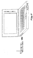
- Figure 3 shows a preferred embodiment of the present invention in the primary mode of voice-operation.
- the primary mode of voice-operation is to be used in the event that the host device 13 is equipped with the proper sound hardware 14, which is constituted by a microphone 15 and a speaker 16 along with an A/D 17 and a D/A 18 converter which can be driven simultaneously, thereby providing a full-duplex sound path.
- the speech from the user will be picked up by the host device's microphone and converted to digital samples by the A/D converter.
- the digital samples are first compressed using a compression technology on the host device, after which the compressed speech data is routed to the control module 3 through the host interface 4. This situation is graphically depicted in figure 2.
- Figure 2 also shows the present invention when used for data-communication.
- the present invention will mimic the operation of a normal modem connected to the fixed telephone network, with some additions with respect to network, security and usability aspects.
- these additional features are network specific and need not be present in every implementation.
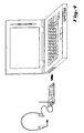
- Figure 5 shows a preferred embodiment of the present invention in the alternate mode of voice-operation.
- This mode is to be used in the event that the host device is not equipped with the proper sound hardware.
- an ordinary headset carrying a microphone and a speaker can be plugged in the telecommunications card according to the present invention to provide the means for voice-communication.
- the invention still has to be attached to a host device through the host interface 4 because it is controlled from the host device. This situation is graphically depicted in figure 4.
- the host interface 4 complies with a widely used and accepted electrical and mechanical standard such as the PCMCIA 2.0.
- the PCMCIA standard has been chosen for its widely acceptance in the industry, however another kind of connection can equally be used.
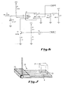
- circuitry to be provided in the telecommunication card for managing the power coming from the power source of the host device.
- the heart of this circuit is the current limiting device U1.
- the current limiting device is connected between the PCMCIA connector and the RF section.
- a current is supplied from the power source of the host device (indicated by VCC) to an input IN1.
- the current limiting device takes care that this current does not exceed a maximal value I MAX , which is set by device U1.
- the input IN1 is connected to the power source via a self L1 and parallel connection of two capacitors C1 and C2.
- L1, C1 and C2 form a low-pass filter which prevents that signals originating from the current limiter would be superposed on the VCC power of the host device and damage the latter.
- the current arriving in IN1 passes through the current limiting device and is supplied to the output OUT1 which delivers current to the components of the telecommunications card, in particular the RF section.
- the current output at OUT1 is supplied to capacitor C3 in order to charge this capacitor.
- the capacitor C3 is formed by a number of capacitors connected in parallel. A parallel connection of capacitors enables to provide sufficient storage capacity while remaining within dimension constraints.
- Capacitor C3 is also connected to the RF section.
- the capacitor C3 has for example a value of 2.2 mF .
- the charge present in capacitor C3 will be used to power the RF-section from the card in combination with the current supplied directly through path IN1/OUT1.
- the device U1 can be completely turned off by means of the ON/OFF input, which can be driven from the control module 3, thereby reducing consumed power. Shutting down U1 will be done whenever the RF-section can be made inactive. In such a manner there is prevented that the inevitable discharge of C3 due to leakage would cause power to be retrieved from the host to compensate the leakage.
- the MODE-input is adjusted when a lower maximum allowed transmitter power level (P TMax ) is set. Proportionally to the voltage present at the MODE-input, transistor Q1 will draw more or less current from U1's SET terminal. This, in its turn, will define the maximum current at the IN1 terminal. Thus, the net effect will be that the maximum current drawn from VCC is set by the voltage present on the MODE-input.
- the MODE-input can be tied to an analog or digital output. In the latter case, only two levels of PTMax are possible.
- the resistors R1 to R4 have to be chosen in such a way that the current to the RF-section is adequate for the chosen transmit power level. Furthermore, the value of C3 has to be chosen so that the charge stored in it is sufficient to supply power to the RF-section during each burst, without the voltage becoming out of specification for that particular RF-section.
- PCMCIA Personal Computer Memory Card Interface Association
- PCMCIA cards provide expansion capability for computers and enable to support several functions such as radio-band fax and modem capabilities, mass storage and memory extension.
- the socket/adapter on the computer has a standard 68-pin interface for the card and the adapter converts the PCMCIA interface signals to match the computer bus standard.
- a PCMCIA card 22 is provided with a SIM card connector such as illustrated in figure 7.
- the connector 6 holds a SIM 21 (Subscriber Identification Module) or UIM (User Identification Module) card.
- SIM 21 Subscriber Identification Module
- UIM User Identification Module
- the PCMCIA card is dimensioned in such a manner as to receive the SIM or UIM card.
- the PCMCIA card has a length of 85.6 mm. The insertion of the SIM card into the PCMCIA card personalises the latter and comprises information that is specific for the particular used PCMCIA card.
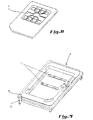
- a standard SIM card as shown in Figure 8, comprises a microchip section 5, onto which data is stored such as identification of the subscriber, address book, ....
- This SIM card is provided to be fitted in the SIM card connector 6, shown in figure 8 and provided to be placed on the PCMCIA card.
- the connector comprises pegs 12 provided to be fitted into corresponding openings in the printed circuit board of the PCMCIA card facilitating the assembling.
- the connector comprises two grooves 7 for receiving contact members of electrically conductive material for achieving an electrical contact between the microchip 5 on the SIM card and the circuitry on the printed circuit board of the PCMCIA card.
- the connector 6 is placed near the 68-pin interface of the PCMCIA card, which interface is situated in the interconnect area 23 of the card. Once mounted in the connector, the SIM card fits completely in the substrate area 24 outside the interconnect area 23. The height of the connector is dimensioned in such a manner that the connector fits into a hole 24 provided in the PCMCIA card. Since the substrate area where the connector is located, is situated outside the RF section 25, crosstalk between the digital signals of the SIM card in the control module situated in the substrate area and the high frequency signals in the RF section is avoided. The signals exchanged between the SIM card and the control module are of low frequency and do not interfere with the high frequency RF signals in the RF section.
- the connector 6 further comprises an upright border 8 provided to be fitted in a corresponding opening provided in a cover of the PCMCIA card, making the holder accessible for inserting and removing a SIM card.
- the corresponding opening is dimensioned in such a manner to correspond to the border of the holder, so that introduction of dust or moisture on the printed circuit board is essentially prevented.
- the height of the connector is dimensioned in such a manner that it is no longer necessary to cut a hole in the substrate in which the connector fits. Only a small perforation for insertion of the pegs 12 is necessary.
- the connector according to the present invention thus no longer requires to apply the "hang in” principle where a hole of a dimension slightly larger than the SIM card is applied on the substrate.
- the connector is dimensioned in such a manner that it fits within the 5 mm height of the PCMCIA card.
- the contact members applied in the grooves 7 are resilient and preferably apply a force of 1,5 N per contact.
- the upright border 8 is also made of resilient material so that the SIM card, once applied in the connector is kept in place by the resilient force applied at the under side by the contact members and at the upper side by the border 8.
- the connector is made of a material having a dielectricum value in such a manner that electrostatic discharge to sensitive components near the connector is substantially reduced.
- the connector forms indeed a dielectricum barrier interrupting a galvanic path towards the control module.
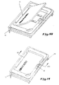
- Figures 10 and 11 illustrate how to insert a SIM card on the connector 6 according to the invention.
- a first border of the SIM card is fitted in a first border 9 of the connector.
- the second border of the card is pushed into the connector.
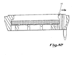
- a latching member 11 On the second border 10 of the connector, there is provided a latching member 11, which is illustrated in Figure 12.
- the latching member When pushing the opposite border of the card, the latching member is displaced away according to the arrow ( Figure 12).
- the resilient force exerted by the contact members also helps to push the SIM card out of the connector.
- the latching member is made of a resilient material, e.g.
- ABS so that it automatically returns to a locking position for locking the SIM card.
- the correct dimensioning of the latching member and the use of resilient material provides a membrane character to the latching member enabling to adequately enclosing the SIM card.
- the SIM card is kept locked in the correct position due to the pressure applied by the resilient material on the card.
Landscapes
- Engineering & Computer Science (AREA)
- Computer Networks & Wireless Communication (AREA)
- Signal Processing (AREA)
- Computer Hardware Design (AREA)
- General Engineering & Computer Science (AREA)
- Theoretical Computer Science (AREA)
- Physics & Mathematics (AREA)
- General Physics & Mathematics (AREA)
- Human Computer Interaction (AREA)
- Mobile Radio Communication Systems (AREA)
- Power Sources (AREA)
- Treatment Of Water By Ion Exchange (AREA)
- Exchange Systems With Centralized Control (AREA)
- Telephone Set Structure (AREA)
Claims (9)
- Telekommunikationskarte, die zum Anschluss an ein ein Verarbeitungsmittel und eine Stromquelle (VCC) umfassendes Host-Gerät, insbesondere an ein PC-Notebook, dient, wobei die Karte einen Bus, an den eine Host-Schnittstelle (4) zum Kommunizieren mit dem Verarbeitungsmittel, ein Steuermittel (3) und ein HF-Abschnitt (1) zum Senden und Empfangen von Signalen angeschlossen sind, umfasst, wobei die Karte zum Empfang von Betriebsstrom von der Stromquelle dient, dadurch gekennzeichnet, dass die Karte ein Strombegrenzungsgerät (U1) mit einem ersten Eingang (IN1) zum Empfang von Strom von der Stromquelle (VCC) und einen ersten Ausgang (OUT1) zum Senden des Stroms an den an den ersten Ausgang (OUT1) angeschlossenen HF-Abschnitt (1) umfasst, wobei das Strombegrenzungsgerät (U1) weiterhin einen zweiten Eingang (IN1) zum Empfangen des Stroms von der Stromquelle (VCC) und einen zweiten Ausgang (OUT1) zum Liefern des Stroms zu Ladezwecken an eine an den zweiten Ausgang (OUT1) und den HF-Abschnitt (1) angeschlossene wiederaufladbare Stromquelle (C3) umfasst, wobei das Strombegrenzungsgerät (U1) Strombegrenzungsmittel zum Begrenzen des von der Stromquelle (VCC) abgerufenen Stroms umfasst, und die wiederaufladbare Stromquelle (C3) dazu dient, ihren zuvor geladenen Strom in Richtung des HF-Abschnitts (1) als Hilfsstrom zusätzlich zu dem vom ersten Ausgang (OUT1) gelieferten Strom auf eine solche Weise abzuladen, dass ein Spitzenstrom an den HF-Abschnitt geliefert wird.
- Telekommunikationskarte nach Anspruch 1, wobei die wiederaufladbare Quelle (C3) eine Anzahl von parallel geschalteten Kondensatoren umfasst.
- Telekommunikationskarte nach Anspruch 1 oder 2, weiterhin umfassend ein Schaltmittel (ON/OFF), welches an das Strombegrenzungsgerät (U1) angeschlossen ist und dazu dient, das Strombegrenzungsgerät (U1) ein- und auszuschalten.
- Telekommunikationskarte nach Anspruch 3, wobei das Steuermittel (3) zum Steuern des Schaltmittels (ON/OFF) dient.
- Telekommunikationskarte nach einem der vorhergehenden Ansprüche, weiterhin umfassend Strompegeleinstellmittel (MODE, Q1, R1-R4), die an das Strombegrenzungsgerät (U1) angeschlossen sind und zum Einstellen eines höchstzulässigen Sender-Strompegels dienen.
- Telekommunikationskarte nach einem der vorhergehenden Ansprüche, umfassend eine Abdeckung zum Umschließen einer Leiterplatte, auf der der Bus bereitgestellt wird, dadurch gekennzeichnet, dass die Karte weiterhin ein SIM-Kartenhaltemittel (6), das auf der Leiterplatte befestigt wird, und die Abdeckung umfasst, und dass in der Abdeckung eine den Abmessungen des SIM-Kartenhaltemittels entsprechende Öffnung vorgesehen ist.
- Telekommunikationskarte nach Anspruch 6, wobei das SIM-Kartenhaltemittel (6) ein Verriegelungsglied (11) umfasst, das dazu dient, zwischen einer offenen Position zum Einsetzen und Herausnehmen einer SIM-Karte (21) und einer geschlossenen Position zum Halten der SIM-Karte (21) im Haltemittel (6) verschoben zu werden.
- Telekommunikationskarte nach Anspruch 6 oder 7, dadurch gekennzeichnet, dass das Verriegelungsglied (11) aus fedemdem Material besteht.
- Telekommunikationskarte nach einem der Ansprüche 6 bis 8, dadurch gekennzeichnet, dass das SIM-Kartenhaltemittel (6) auf der ein Steuermodul (3) einer PCMCIA-Karte tragenden Leiterplatte befestigt wird.
Priority Applications (4)
| Application Number | Priority Date | Filing Date | Title |
|---|---|---|---|
| AT97203557T ATE300812T1 (de) | 1997-11-14 | 1997-11-14 | Telekommunikationskarte |
| ES97203557T ES2247615T3 (es) | 1997-11-14 | 1997-11-14 | Tarjeta de telecomunicaciones. |
| EP97203557A EP0918399B1 (de) | 1997-11-14 | 1997-11-14 | Telekommunikationskarte |
| DE69733822T DE69733822T2 (de) | 1997-11-14 | 1997-11-14 | Telekommunikationskarte |
Applications Claiming Priority (1)
| Application Number | Priority Date | Filing Date | Title |
|---|---|---|---|
| EP97203557A EP0918399B1 (de) | 1997-11-14 | 1997-11-14 | Telekommunikationskarte |
Publications (2)
| Publication Number | Publication Date |
|---|---|
| EP0918399A1 EP0918399A1 (de) | 1999-05-26 |
| EP0918399B1 true EP0918399B1 (de) | 2005-07-27 |
Family
ID=8228928
Family Applications (1)
| Application Number | Title | Priority Date | Filing Date |
|---|---|---|---|
| EP97203557A Expired - Lifetime EP0918399B1 (de) | 1997-11-14 | 1997-11-14 | Telekommunikationskarte |
Country Status (4)
| Country | Link |
|---|---|
| EP (1) | EP0918399B1 (de) |
| AT (1) | ATE300812T1 (de) |
| DE (1) | DE69733822T2 (de) |
| ES (1) | ES2247615T3 (de) |
Families Citing this family (8)
| Publication number | Priority date | Publication date | Assignee | Title |
|---|---|---|---|---|
| US7603139B1 (en) | 1999-03-25 | 2009-10-13 | Kantan Inc. | Methods and apparatus for a flexible wireless communication and cellular telephone system |
| DE60045294D1 (de) | 1999-06-14 | 2011-01-05 | Ntt Docomo Inc | Batterieeinheit und Ladegerät für ein drahtloses Telekommunikationsgerät |
| US6785830B1 (en) * | 2000-07-21 | 2004-08-31 | Sierra Wireless, Inc. | PC radio card capable of operating at a nonstandard power output level by limiting the current being drawn from a power amplifier |
| RU2201650C2 (ru) * | 2001-02-15 | 2003-03-27 | Жуковский Юрий Георгиевич | Средство радиосвязи |
| US20080207268A1 (en) * | 2005-02-17 | 2008-08-28 | Kantan Inc. | Apparatus for a Removable Wireless Module With Storage Memory |
| CN100403234C (zh) * | 2005-05-24 | 2008-07-16 | 纬创资通股份有限公司 | 利用pcmcia插槽提供电力的方法与系统 |
| US20070082661A1 (en) * | 2005-10-11 | 2007-04-12 | Black Greg R | Method and apparatus for configuration of modular devices |
| EP2319139A4 (de) * | 2008-07-29 | 2014-05-07 | Novatel Wireless Inc | Drahtlose vorrichtung und anordnung |
Family Cites Families (4)
| Publication number | Priority date | Publication date | Assignee | Title |
|---|---|---|---|---|
| JPH04315320A (ja) * | 1991-04-15 | 1992-11-06 | Sony Corp | バースト無線通信装置 |
| FI90298C (fi) * | 1992-02-18 | 1994-01-10 | Nokia Mobile Phones Ltd | Kortinlukijalaite |
| DE59304234D1 (de) * | 1992-03-20 | 1996-11-28 | Siemens Ag | Schaltungsanordnung zur Überbrückung von kurzzeitigen Spannungsabfällen in batteriegespeisten Funkgeräten |
| AU2904995A (en) * | 1994-06-16 | 1996-01-05 | Apple Computer, Inc. | A pc card cellular-based communication system |
-
1997
- 1997-11-14 ES ES97203557T patent/ES2247615T3/es not_active Expired - Lifetime
- 1997-11-14 AT AT97203557T patent/ATE300812T1/de not_active IP Right Cessation
- 1997-11-14 DE DE69733822T patent/DE69733822T2/de not_active Expired - Lifetime
- 1997-11-14 EP EP97203557A patent/EP0918399B1/de not_active Expired - Lifetime
Also Published As
| Publication number | Publication date |
|---|---|
| DE69733822D1 (de) | 2005-09-01 |
| ES2247615T3 (es) | 2006-03-01 |
| ATE300812T1 (de) | 2005-08-15 |
| DE69733822T2 (de) | 2006-04-13 |
| EP0918399A1 (de) | 1999-05-26 |
Similar Documents
| Publication | Publication Date | Title |
|---|---|---|
| JP2833397B2 (ja) | 携帯機 | |
| US5924044A (en) | Modular communication device and method of providing communications therewith | |
| US6452402B1 (en) | Apparatus for determining the type of external device being connected | |
| KR100230553B1 (ko) | 보조 전원을 갖춘 무선 모뎀 | |
| US6509659B1 (en) | Cable or module identification apparatus and method | |
| US5649001A (en) | Method and apparatus for adapting a communication interface device to multiple networks | |
| CA2144148C (en) | Ic card-type radio communication device | |
| US5701515A (en) | Interface for switching plurality of pin contacts to transmit data line and plurality of pin contacts to receive data line to interface with serial controller | |
| US6424842B1 (en) | Dual function connector for cellular phones | |
| US6934561B2 (en) | Cable or module identification apparatus and method | |
| GB2229340A (en) | Radio telephone automatically taking handset number | |
| CA2154318A1 (en) | Adaptable radio telephone handset | |
| PL180449B1 (pl) | Elektroniczne urzadzenie do telekomunikacji PL PL PL | |
| JPH11284543A (ja) | 携帯電子装置のための電子回路 | |
| EP0629071A1 (de) | Einrichtung zum Anschliessen eines Komputers an ein Telefonsystem | |
| EP0918399A1 (de) | Telekommunikationskarte | |
| WO1995034958A1 (en) | A pc card cellular-based communication system | |
| GB2322504A (en) | Tri-fold cellular telephone | |
| JPH10210550A (ja) | 複合携帯端末装置 | |
| EP1125368B1 (de) | Batteriegehäuse für pcmcia-karten-modem mit antenne | |
| KR100825200B1 (ko) | 이동 통신 장치 및 이동 통신 장치용 보조 유닛 | |
| US5336984A (en) | Electronic device powering system | |
| US6246600B1 (en) | Multi-use battery | |
| JPH10116666A (ja) | 携帯型電話機のデータ通信用接続分岐装置 | |
| US20020160792A1 (en) | Device for cordlessly interfacing a computer with a phone line |
Legal Events
| Date | Code | Title | Description |
|---|---|---|---|
| PUAI | Public reference made under article 153(3) epc to a published international application that has entered the european phase |
Free format text: ORIGINAL CODE: 0009012 |
|
| AK | Designated contracting states |
Kind code of ref document: A1 Designated state(s): AT BE CH DE DK ES FI FR GB GR IE IT LI NL PT SE |
|
| AX | Request for extension of the european patent |
Free format text: AL;LT;LV;MK;RO;SI |
|
| 17P | Request for examination filed |
Effective date: 19991125 |
|
| AKX | Designation fees paid |
Free format text: AT BE CH DE DK ES FI FR GB GR IE IT LI NL PT SE |
|
| 17Q | First examination report despatched |
Effective date: 20031022 |
|
| RAP1 | Party data changed (applicant data changed or rights of an application transferred) |
Owner name: OPTION |
|
| GRAP | Despatch of communication of intention to grant a patent |
Free format text: ORIGINAL CODE: EPIDOSNIGR1 |
|
| GRAS | Grant fee paid |
Free format text: ORIGINAL CODE: EPIDOSNIGR3 |
|
| GRAA | (expected) grant |
Free format text: ORIGINAL CODE: 0009210 |
|
| AK | Designated contracting states |
Kind code of ref document: B1 Designated state(s): AT BE CH DE DK ES FI FR GB GR IE IT LI NL PT SE |
|
| PG25 | Lapsed in a contracting state [announced via postgrant information from national office to epo] |
Ref country code: LI Free format text: LAPSE BECAUSE OF FAILURE TO SUBMIT A TRANSLATION OF THE DESCRIPTION OR TO PAY THE FEE WITHIN THE PRESCRIBED TIME-LIMIT Effective date: 20050727 Ref country code: FI Free format text: LAPSE BECAUSE OF FAILURE TO SUBMIT A TRANSLATION OF THE DESCRIPTION OR TO PAY THE FEE WITHIN THE PRESCRIBED TIME-LIMIT Effective date: 20050727 Ref country code: CH Free format text: LAPSE BECAUSE OF FAILURE TO SUBMIT A TRANSLATION OF THE DESCRIPTION OR TO PAY THE FEE WITHIN THE PRESCRIBED TIME-LIMIT Effective date: 20050727 Ref country code: AT Free format text: LAPSE BECAUSE OF FAILURE TO SUBMIT A TRANSLATION OF THE DESCRIPTION OR TO PAY THE FEE WITHIN THE PRESCRIBED TIME-LIMIT Effective date: 20050727 |
|
| REG | Reference to a national code |
Ref country code: GB Ref legal event code: FG4D |
|
| REG | Reference to a national code |
Ref country code: CH Ref legal event code: EP |
|
| RAP2 | Party data changed (patent owner data changed or rights of a patent transferred) |
Owner name: OPTION |
|
| REG | Reference to a national code |
Ref country code: IE Ref legal event code: FG4D |
|
| REF | Corresponds to: |
Ref document number: 69733822 Country of ref document: DE Date of ref document: 20050901 Kind code of ref document: P |
|
| PG25 | Lapsed in a contracting state [announced via postgrant information from national office to epo] |
Ref country code: SE Free format text: LAPSE BECAUSE OF FAILURE TO SUBMIT A TRANSLATION OF THE DESCRIPTION OR TO PAY THE FEE WITHIN THE PRESCRIBED TIME-LIMIT Effective date: 20051027 Ref country code: GR Free format text: LAPSE BECAUSE OF FAILURE TO SUBMIT A TRANSLATION OF THE DESCRIPTION OR TO PAY THE FEE WITHIN THE PRESCRIBED TIME-LIMIT Effective date: 20051027 Ref country code: DK Free format text: LAPSE BECAUSE OF FAILURE TO SUBMIT A TRANSLATION OF THE DESCRIPTION OR TO PAY THE FEE WITHIN THE PRESCRIBED TIME-LIMIT Effective date: 20051027 |
|
| NLT2 | Nl: modifications (of names), taken from the european patent patent bulletin |
Owner name: OPTION Effective date: 20050824 |
|
| PG25 | Lapsed in a contracting state [announced via postgrant information from national office to epo] |
Ref country code: IE Free format text: LAPSE BECAUSE OF NON-PAYMENT OF DUE FEES Effective date: 20051114 |
|
| PG25 | Lapsed in a contracting state [announced via postgrant information from national office to epo] |
Ref country code: PT Free format text: LAPSE BECAUSE OF FAILURE TO SUBMIT A TRANSLATION OF THE DESCRIPTION OR TO PAY THE FEE WITHIN THE PRESCRIBED TIME-LIMIT Effective date: 20051227 |
|
| REG | Reference to a national code |
Ref country code: CH Ref legal event code: PL |
|
| REG | Reference to a national code |
Ref country code: ES Ref legal event code: FG2A Ref document number: 2247615 Country of ref document: ES Kind code of ref document: T3 |
|
| ET | Fr: translation filed | ||
| PLBE | No opposition filed within time limit |
Free format text: ORIGINAL CODE: 0009261 |
|
| STAA | Information on the status of an ep patent application or granted ep patent |
Free format text: STATUS: NO OPPOSITION FILED WITHIN TIME LIMIT |
|
| 26N | No opposition filed |
Effective date: 20060428 |
|
| REG | Reference to a national code |
Ref country code: IE Ref legal event code: MM4A |
|
| BECA | Be: change of holder's address |
Owner name: *OPTIONKOLONEL BEGAULTLAAN 45, B-3012 LEUVEN Effective date: 20050727 |
|
| PGFP | Annual fee paid to national office [announced via postgrant information from national office to epo] |
Ref country code: FR Payment date: 20121002 Year of fee payment: 16 |
|
| PGFP | Annual fee paid to national office [announced via postgrant information from national office to epo] |
Ref country code: BE Payment date: 20121005 Year of fee payment: 16 Ref country code: DE Payment date: 20121121 Year of fee payment: 16 Ref country code: NL Payment date: 20120924 Year of fee payment: 16 |
|
| PGFP | Annual fee paid to national office [announced via postgrant information from national office to epo] |
Ref country code: GB Payment date: 20121120 Year of fee payment: 16 Ref country code: ES Payment date: 20121127 Year of fee payment: 16 Ref country code: IT Payment date: 20121123 Year of fee payment: 16 |
|
| BERE | Be: lapsed |
Owner name: *OPTION Effective date: 20131130 |
|
| REG | Reference to a national code |
Ref country code: DE Ref legal event code: R119 Ref document number: 69733822 Country of ref document: DE |
|
| REG | Reference to a national code |
Ref country code: NL Ref legal event code: V1 Effective date: 20140601 |
|
| GBPC | Gb: european patent ceased through non-payment of renewal fee |
Effective date: 20131114 |
|
| REG | Reference to a national code |
Ref country code: FR Ref legal event code: ST Effective date: 20140731 |
|
| PG25 | Lapsed in a contracting state [announced via postgrant information from national office to epo] |
Ref country code: NL Free format text: LAPSE BECAUSE OF NON-PAYMENT OF DUE FEES Effective date: 20140601 Ref country code: DE Free format text: LAPSE BECAUSE OF NON-PAYMENT OF DUE FEES Effective date: 20140603 Ref country code: IT Free format text: LAPSE BECAUSE OF NON-PAYMENT OF DUE FEES Effective date: 20131114 |
|
| REG | Reference to a national code |
Ref country code: DE Ref legal event code: R119 Ref document number: 69733822 Country of ref document: DE Effective date: 20140603 |
|
| PG25 | Lapsed in a contracting state [announced via postgrant information from national office to epo] |
Ref country code: BE Free format text: LAPSE BECAUSE OF NON-PAYMENT OF DUE FEES Effective date: 20131130 |
|
| PG25 | Lapsed in a contracting state [announced via postgrant information from national office to epo] |
Ref country code: FR Free format text: LAPSE BECAUSE OF NON-PAYMENT OF DUE FEES Effective date: 20131202 Ref country code: GB Free format text: LAPSE BECAUSE OF NON-PAYMENT OF DUE FEES Effective date: 20131114 |
|
| REG | Reference to a national code |
Ref country code: ES Ref legal event code: FD2A Effective date: 20150406 |
|
| PG25 | Lapsed in a contracting state [announced via postgrant information from national office to epo] |
Ref country code: ES Free format text: LAPSE BECAUSE OF NON-PAYMENT OF DUE FEES Effective date: 20131115 |