EP0919985A1 - Dispositif et procede de conversion de balayage - Google Patents
Dispositif et procede de conversion de balayage Download PDFInfo
- Publication number
- EP0919985A1 EP0919985A1 EP98919540A EP98919540A EP0919985A1 EP 0919985 A1 EP0919985 A1 EP 0919985A1 EP 98919540 A EP98919540 A EP 98919540A EP 98919540 A EP98919540 A EP 98919540A EP 0919985 A1 EP0919985 A1 EP 0919985A1
- Authority
- EP
- European Patent Office
- Prior art keywords
- signal
- frequency
- image signal
- clock pulses
- horizontal
- Prior art date
- Legal status (The legal status is an assumption and is not a legal conclusion. Google has not performed a legal analysis and makes no representation as to the accuracy of the status listed.)
- Withdrawn
Links
Images




Classifications
-
- H—ELECTRICITY
- H04—ELECTRIC COMMUNICATION TECHNIQUE
- H04N—PICTORIAL COMMUNICATION, e.g. TELEVISION
- H04N7/00—Television systems
- H04N7/01—Conversion of standards, e.g. involving analogue television standards or digital television standards processed at pixel level
-
- G—PHYSICS
- G09—EDUCATION; CRYPTOGRAPHY; DISPLAY; ADVERTISING; SEALS
- G09G—ARRANGEMENTS OR CIRCUITS FOR CONTROL OF INDICATING DEVICES USING STATIC MEANS TO PRESENT VARIABLE INFORMATION
- G09G5/00—Control arrangements or circuits for visual indicators common to cathode-ray tube indicators and other visual indicators
- G09G5/36—Control arrangements or circuits for visual indicators common to cathode-ray tube indicators and other visual indicators characterised by the display of a graphic pattern, e.g. using an all-points-addressable [APA] memory
- G09G5/39—Control of the bit-mapped memory
- G09G5/391—Resolution modifying circuits, e.g. variable screen formats
-
- G—PHYSICS
- G09—EDUCATION; CRYPTOGRAPHY; DISPLAY; ADVERTISING; SEALS
- G09G—ARRANGEMENTS OR CIRCUITS FOR CONTROL OF INDICATING DEVICES USING STATIC MEANS TO PRESENT VARIABLE INFORMATION
- G09G3/00—Control arrangements or circuits, of interest only in connection with visual indicators other than cathode-ray tubes
- G09G3/20—Control arrangements or circuits, of interest only in connection with visual indicators other than cathode-ray tubes for presentation of an assembly of a number of characters, e.g. a page, by composing the assembly by combination of individual elements arranged in a matrix no fixed position being assigned to or needed to be assigned to the individual characters or partial characters
- G09G3/2092—Details of a display terminals using a flat panel, the details relating to the control arrangement of the display terminal and to the interfaces thereto
-
- H—ELECTRICITY
- H04—ELECTRIC COMMUNICATION TECHNIQUE
- H04N—PICTORIAL COMMUNICATION, e.g. TELEVISION
- H04N7/00—Television systems
- H04N7/01—Conversion of standards, e.g. involving analogue television standards or digital television standards processed at pixel level
- H04N7/0105—Conversion of standards, e.g. involving analogue television standards or digital television standards processed at pixel level using a storage device with different write and read speed
-
- G—PHYSICS
- G09—EDUCATION; CRYPTOGRAPHY; DISPLAY; ADVERTISING; SEALS
- G09G—ARRANGEMENTS OR CIRCUITS FOR CONTROL OF INDICATING DEVICES USING STATIC MEANS TO PRESENT VARIABLE INFORMATION
- G09G2360/00—Aspects of the architecture of display systems
- G09G2360/18—Use of a frame buffer in a display terminal, inclusive of the display panel
-
- G—PHYSICS
- G09—EDUCATION; CRYPTOGRAPHY; DISPLAY; ADVERTISING; SEALS
- G09G—ARRANGEMENTS OR CIRCUITS FOR CONTROL OF INDICATING DEVICES USING STATIC MEANS TO PRESENT VARIABLE INFORMATION
- G09G5/00—Control arrangements or circuits for visual indicators common to cathode-ray tube indicators and other visual indicators
- G09G5/003—Details of a display terminal, the details relating to the control arrangement of the display terminal and to the interfaces thereto
- G09G5/006—Details of the interface to the display terminal
-
- G—PHYSICS
- G09—EDUCATION; CRYPTOGRAPHY; DISPLAY; ADVERTISING; SEALS
- G09G—ARRANGEMENTS OR CIRCUITS FOR CONTROL OF INDICATING DEVICES USING STATIC MEANS TO PRESENT VARIABLE INFORMATION
- G09G5/00—Control arrangements or circuits for visual indicators common to cathode-ray tube indicators and other visual indicators
- G09G5/003—Details of a display terminal, the details relating to the control arrangement of the display terminal and to the interfaces thereto
- G09G5/006—Details of the interface to the display terminal
- G09G5/008—Clock recovery
-
- H—ELECTRICITY
- H04—ELECTRIC COMMUNICATION TECHNIQUE
- H04N—PICTORIAL COMMUNICATION, e.g. TELEVISION
- H04N5/00—Details of television systems
- H04N5/04—Synchronising
- H04N5/12—Devices in which the synchronising signals are only operative if a phase difference occurs between synchronising and synchronised scanning devices, e.g. flywheel synchronising
- H04N5/126—Devices in which the synchronising signals are only operative if a phase difference occurs between synchronising and synchronised scanning devices, e.g. flywheel synchronising whereby the synchronisation signal indirectly commands a frequency generator
Definitions
- This invention relates to a scan converting device and a scan converting method for converting horizontal scanning frequency of computer display signals and input image signals of high fidelity television sets, and more particularly, to a device and a method enabling horizontal size adjustment in addition to scan conversion.
- Recent image signal sources range over a variety of sorts. Especially in computer displays, many kinds of scanning frequencies are used, and there are cases using a plurality of scanning frequencies in a single computer. Therefore, display apparatuses are required to have a multi-scanning deflection system. On the other hand, display screens have come to diversify in size. Especially, the demand for large-scale displays is increasing progressively, and display of computer signals by a large-scale projector has become active.
- An existing scheme is to fix the deflection frequency to a single frequency, such as 60 Hz/31.5 kHz, and to process and convert various sorts of image signals into image signals of the single scanning frequency.
- a frequency converter 40 Introduced into a frequency converter 40 are three kinds of image signals different in scanning frequency, for example, ordinary NTSC signal (field frequency 59.9 Hz and horizontal scanning frequency 15.734), SVGA computer signal whose field frequency ranges from 50 Hz to 70 Hz and whose horizontal scanning frequency ranges from 35 kHz to 50 kHz, and HDTV signal having the field frequency of 60 Hz and the horizontal scanning frequency of 33.75 kHz.
- the frequency converter 40 converts the input image signals into image signals of a single scanning frequency 60Hz/35.5kHz, and supplies these image signals to a display apparatus.
- Fig. 2 shows a system in which an NTSC signal with 240 scanning lines, SVGA signal with 600 scanning lines and HDTV with 518 scanning lines are scan-converted by a frequency converter 40. Scan-converted image signals are displayed on a display apparatus, such as plasma display apparatus, having fixed pixels of 640 dots by 480 lines.
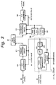
- Fig. 3 is a block diagram showing a main construction for scan conversion which has been used to date.
- the "scan conversion” pertains to converting, for example, a SVGA signal (800 pixels by 600 lines) into a VGA signal (640 pixels by 480 lines).
- an input image signal 50 is converted into a digital signal by an A/D converter 26, and provisionally stored in a field memory 20 which is configured to write data of the effective image period in one horizontal (1H) period.
- An independent sync signal asynchronous with the input image signal 50 is created from clock pulses 62 by a sync signal generator 38.
- An image signal is read out from the field memory 20 by clock pulses 62, and it is converted into an analog signal by a D/A converter 36.
- a primary processing circuit 27 is provided on the write side of the field memory 20, and a secondary processing circuit 37 is provided on the read side thereof.
- the primary processing circuit 27 conducts vertical interpolation processing to convert, for example, 600 lines into 480 lines.
- the secondary processing circuit 37 adds a horizontal sync signal and a vertical sync signal.
- a PLL circuit 21 is provided to generate a sampling clock for the A/D converter 26.
- the PLL circuit 21 includes a phase comparator 22, low pass filter (LPF) 23, voltage control oscillator (hereinafter abbreviated to VCO) 24, and frequency divider 25.
- the PLL circuit 21 generates a clock pulse 52 synchronous with the horizontal sync signal 51 of the input image signal 50.
- A/D conversion or other processing prior to clock re-riding is conducted by the clock pulse 52.
- the secondary processing circuit 37 uses a clock pulse 62 output from a free-run clock generator 39.
- the clock generator 39 is a quarts oscillator which stably generates clock pulses.
- the output side sync signal is made in the sync signal generator 38 by using the clock pulse 62, and does not synchronize with the input side sync signal.
- the scan converting device functions to adjust the horizontal size of the display screen.
- the number of pixels corresponding to the effective image period is not always a predetermined number (for example, 640).
- the display apparatus often fails to display the full extent of the effective image period but often drops edge portions thereof. Since representation of panels, icons, and so fourth, typically lies along edges of computer displays, failure to represent these things degrades the manipulative performance.
- computer displays are configured to permit a user to appropriately adjust the horizontal width of the display screen in addition to the scan conversion. This adjustment is called horizontal size adjustment.
- the horizontal size is adjustable by adjusting the amplitude of horizontal deflection.
- pixel-fixed displays like that shown in Fig. 2 cannot use the same method for horizontal size adjustment, and relies on signal processing for horizontal size adjustment.
- CRT displays using beam deflection can employ horizontal size adjustment by signal processing as well.
- the scan conversion device shown in Fig. 3 can adjust the horizontal size. More specifically, by introducing an external UP/DOWN signal increasing or decreasing the frequency division ratio into the frequency divider 25 and by changing the ratio of oscillation frequency of VCO 24 relative to the horizontal scanning frequency of the input image signal, the number of sampling in one horizontal period of the input image signal can be changed. On the other hand, the number of sampling in one horizontal period at the output side (read-out side) is held always constant. For example, if the frequency division ration of the frequency divider 25 is 1/800, then the number of sampling of one horizontal period of the input image signal is 800. If the frequency division ration is made larger than 1/800, the frequency of the sampling clock becomes high, the number of sampling of one horizontal period becomes larger than 800, and the number of pixels in the effective image period increases.
- the number of pixels in the effective screen relative to the sampling number of one horizontal period is changed by adjusting the frequency of the sampling clock of the A/D converter 26.
- the length of the effective image period relative to one horizontal period is changed, and the horizontal size can be adjusted correlatively.
- This method for horizontal adjustment fixes the sampling number of one horizontal period on the output side always constant, and changes the number of pixels in the effective image period per one line of the input image signal.
- the number of pixels relative to the effective screen of the input image signal also changes. That is, horizontal size adjustment invites a change in sampling point (sampling phase) for sampling by the A/D converter 26, and deteriorates the quality of images in case of signals with a high horizontal frequency (for example, signals of fine characters). Since typical computer signals are for representation of fine characters, this is a serious problem.
- the field memory 20 for synchronous re-riding is required to have a much larger capacitance to allow for a margin beforehand.
- a scan converting device for converting the scanning frequency for an analog input image signal and for outputting an image display signal, comprising:
- the scan converting device may further comprise a sync signal generating circuit for generating a vertical sync signal and a horizontal sync signal which are asynchronous with the input image signal, the second clock pulses being synchronous with the horizontal sync signal.
- a frequency divider may be further provided for dividing an oscillation output of a voltage control oscillator of the second PLL circuit in frequency so as to obtain second clock pulses with a frequency corresponding to the frequency division ratio from the voltage control oscillator.
- a scan converting method for converting the scanning frequency for an analog input image signal and for outputting an image display signal comprising:
- the clock frequency read out from the field memory is changed.
- the sampling number in one horizontal period during reading is changed.
- the number of pixels in the effective image period in one horizontal period on the part of writing onto the field memory does not change. Therefore, the output image signal results in being controlled in ratio of the length of the effective image period in one horizontal period. That is, the horizontal size is adjusted. Since the image signal is digitalized in a constant sampling phase on the part of writing, quality deterioration of images die to changes in sampling phase can be prevented.
- FIG. 4 is a block diagram showing a central construction of a scanning line converting device taken as an embodiment of the invention.
- horizontal size of a display screen is adjusted by using a scan converting device.
- the scanning line converting device includes an A/D converter 6 for converting an input image signal into a digital form, PLL circuit 1 for creating clock pulses 53 for the A/D converter 6, field memory 10, D/A converter 16 for returning a signal read out from the field memory 10 into an analog form, PLL circuit 11 for creating clock pulses 63 used in the D/A converter 16, etc., sync signal generator 18 for creating a sync signal synchronous with the clock pulses 63, clock generator 19 for generating clock pulses which is the base of the sync signal, primary processing circuit 7 for converting the number of scanning lines, and secondary processing circuit 17 for adding sync signals.
- A/D converter 6 for converting an input image signal into a digital form
- PLL circuit 1 for creating clock pulses 53 for the A/D converter 6, field memory 10, D/A converter 16 for returning a signal read out from the field memory 10 into an analog form
- PLL circuit 11 for creating clock pulses 63 used in the D/A converter 16, etc.
- sync signal generator 18 for creating a sync signal
- the field memory 10 is configured to write data of the effective image period therein. However, it may be configured to store data of the entirety of one horizontal period.
- PLL circuits 1 and 11 are widely used ones, each including a phase comparator 2 or 12, LPF 3 or 13, VCO 4 or 14 and frequency divider 5 or 15, and only the frequency divider 15 in the read-side PLL circuit 11 is externally adjustable in frequency division ratio.
- the frequency division ratio of the frequency divider 15 can be adjusted by supplying an UP signal for heightening the frequency division ratio or a DOWN signal for lowering it through a remote control signal, for example, to change the reset value in a counter (not shown) in the frequency divider 15.
- the PLL circuit 1 creates a sampling clock for A/D conversion and also creates a clock for the primary processing circuit 7 and a write clock for the field memory 10.
- the PLL circuit 11 creates a read clock for the field memory 10, a clock for the secondary processing circuit 17, and a clock for D/A conversion.
- the input image signal 50 is converted into a digital form by the A/D converter 6, then passed through the primary processing circuit 7, and provisionally stored in the field memory 10. It is read out with clock pulses 63 asynchronous with the horizontal sync signal 51 prior to conversion, and then passed through the secondary processing circuit 17, and returned to and output as an analog signal by the D/A converter 16.
- computer signals with horizontal scanning frequencies from 31.5 kHz to 90 kHz are displayed on a display apparatus whose horizontal frequency (fixed) is 31.5 kHz.
- the frequency division ration of the frequency divider in the PLL circuit 1 be a fixed value.
- the PLL circuit 1 divides an oscillation output of VCO 4 in frequency, and compares its phase with the horizontal sync signal 51 in the phase comparator 2, and feeds an error signal back to VCO 4 via LPF 3 to establish synchronization between clock pulses 53 and the horizontal sync signal 51.
- the oscillation output from VCO 4 are used as clock pulses 53 for A/D conversion.
- the SVGA signal is digitalized so that the sampling number of one horizontal period be 800 and the number of pixels in the effective image period be approximately 640. Since the number of pixels may differ among input image signals, horizontal size adjustment is indispensable.
- the block construction of the PLL circuit on the read-out side of the field memory 10 is the same as that of the PLL circuit 1; however, the frequency division ratio of the frequency divider 15 is variable.
- the frequency division ratio has a variable range of 1/700 to 1/1000.
- the oscillation output from VCO 14 is counted down to the horizontal scanning frequency (for example, 31.5 kHz) by the frequency divider 15, then introduced into the phase comparator 12, and compared there in phase with a horizontal sync signal 61 generated by the sync signal generator 18 independently from the horizontal sync signal 51, and an error signal resulting from the comparison is fed back to VCO 14 via LPF 13.
- the oscillation output of VCO 14, i.e. clock pulses 63 are synchronous with the horizontal sync signal 61, but independent from the input-side horizontal sync signal 51.
- clock pulses 63 By reading out the image signal from the field memory 10 at a new timing made by the clock pulses 63 and a horizontal sync signal 61 and a vertical sync signal 64 generated by the sync signal generator 18, synchronous re-riding is executed.
- the primary processing circuit 7 and the secondary processing circuit 17 are provided before and after the field memory 10.
- the primary processing circuit 7 performs conversion of the number of scanning lines whereas the secondary processing circuit 17 performs addition of sync signals.
- filtering process may be added in order to prevent deterioration of the quality of images which may occur upon signal processing for analog or digital conversion.
- the horizontal sync signal 61 and the vertical sync signal 64 created by the sync signal generator 18 based on the output pulses from the clock generator 19 are supplied to a deflection circuit system (not shown), or the like, which may be provided in the display apparatus, where necessary, to drive the display apparatus together with the output signal from the D/A converter 16 so as to display images on the display screen.
- the sampling number of one horizontal period upon A/D conversion of the input image signal 50 is always a constant value (800) because the frequency division ratio of the frequency divider 5 is 1/800.
- the sampling point (sampling phase) for signals in the effective image period becomes a predetermined phase locked at the horizontal sync signal, and approximately 640 pixels exist in the effective image period in case of a VGA signal.
- the sampling number of one horizontal period for reading from the field memory 10 can be changed in the range of 700 to 1000 by externally adjusting the frequency division ratio of the frequency divider 15 in the range of 1/700 to 1/1000.
- the sampling number of one horizontal period for reading can be set in 900.
- Fig. 5 schematically shows horizontal size adjustment according to an embodiment of the invention.
- Fig. 5A shows a case where the sampling number in one horizontal period on the output side is increased to 800+ ⁇ by increasing the frequency division ratio of the frequency divider 15 than 1/800. In this case, the effective image period in one horizontal period becomes relatively shorter, and the horizontal size becomes smaller accordingly.
- the sampling number in one period on the output side can be decreased to 800- ⁇ as shown in Fig. 5B.
- the horizontal size can be enlarged.
- the present invention is applicable to plasma displays, liquid crystal displays, liquid crystal projectors and CRT displays.
- the invention enables signal processing for converting scanning frequencies and horizontal size adjustment while preventing deterioration of the quality images for image signals of a wide variety of horizontal scanning frequencies.
Landscapes
- Engineering & Computer Science (AREA)
- Physics & Mathematics (AREA)
- Computer Hardware Design (AREA)
- General Physics & Mathematics (AREA)
- Theoretical Computer Science (AREA)
- Multimedia (AREA)
- Signal Processing (AREA)
- Controls And Circuits For Display Device (AREA)
- Transforming Electric Information Into Light Information (AREA)
- Television Systems (AREA)
- Television Signal Processing For Recording (AREA)
Applications Claiming Priority (3)
| Application Number | Priority Date | Filing Date | Title |
|---|---|---|---|
| JP9126940A JPH10319932A (ja) | 1997-05-16 | 1997-05-16 | ディスプレイ装置 |
| JP126940/97 | 1997-05-16 | ||
| PCT/JP1998/002065 WO1998052183A1 (fr) | 1997-05-16 | 1998-05-11 | Dispositif et procede de conversion de balayage |
Publications (2)
| Publication Number | Publication Date |
|---|---|
| EP0919985A1 true EP0919985A1 (fr) | 1999-06-02 |
| EP0919985A4 EP0919985A4 (fr) | 2005-06-15 |
Family
ID=14947674
Family Applications (1)
| Application Number | Title | Priority Date | Filing Date |
|---|---|---|---|
| EP98919540A Withdrawn EP0919985A4 (fr) | 1997-05-16 | 1998-05-11 | Dispositif et procede de conversion de balayage |
Country Status (5)
| Country | Link |
|---|---|
| US (1) | US6285402B1 (fr) |
| EP (1) | EP0919985A4 (fr) |
| JP (1) | JPH10319932A (fr) |
| KR (1) | KR20000023800A (fr) |
| WO (1) | WO1998052183A1 (fr) |
Cited By (1)
| Publication number | Priority date | Publication date | Assignee | Title |
|---|---|---|---|---|
| WO2006068358A1 (fr) * | 2004-12-21 | 2006-06-29 | Samsung Electronics Co., Ltd. | Appareil d'affichage, methode de commande de cet appareil et dispositif pour traiter un signal |
Families Citing this family (15)
| Publication number | Priority date | Publication date | Assignee | Title |
|---|---|---|---|---|
| US6480545B1 (en) * | 1999-08-11 | 2002-11-12 | Grass Valley (U.S.) Inc. | Architecture for multi-format video processing |
| JP2001333392A (ja) * | 2000-05-23 | 2001-11-30 | Matsushita Electric Ind Co Ltd | 水平偏向回路およびテレビジョン受像機 |
| JP2002101316A (ja) * | 2000-09-26 | 2002-04-05 | Mitsubishi Electric Corp | クロック生成回路及び画像表示装置 |
| TW563353B (en) * | 2002-03-12 | 2003-11-21 | Via Tech Inc | Clock signal synthesizer with multiple frequency outputs and method for synthesizing clock signal |
| TW561783B (en) * | 2002-03-12 | 2003-11-11 | Via Tech Inc | Image processing method and device |
| TW527824B (en) * | 2002-03-12 | 2003-04-11 | Via Tech Inc | Adative-deflicker processing method and adaptive deflicker filter |
| JP3922252B2 (ja) * | 2003-03-04 | 2007-05-30 | ソニー株式会社 | 映像信号処理回路、映像信号処理方法 |
| US7170469B2 (en) * | 2003-07-18 | 2007-01-30 | Realtek Semiconductor Corp. | Method and apparatus for image frame synchronization |
| US20050052386A1 (en) * | 2003-08-28 | 2005-03-10 | Su-Hyun Kwon | Method of processing image signals for improved image quality |
| US7091967B2 (en) * | 2003-09-01 | 2006-08-15 | Realtek Semiconductor Corp. | Apparatus and method for image frame synchronization |
| JP2005099516A (ja) * | 2003-09-25 | 2005-04-14 | Sony Corp | 画像処理回路および画像表示装置 |
| US7355652B2 (en) * | 2004-10-13 | 2008-04-08 | Cirrus Logic, Inc. | Inverse tracking over two different clock domains |
| TWI249359B (en) * | 2004-12-22 | 2006-02-11 | Realtek Semiconductor Corp | Method and apparatus for simultaneous progressive and interlaced display |
| JP2006235129A (ja) * | 2005-02-23 | 2006-09-07 | Matsushita Electric Ind Co Ltd | 映像信号処理装置 |
| US9066076B2 (en) * | 2009-10-30 | 2015-06-23 | Mitsubishi Electric Corporation | Video display control method and apparatus |
Family Cites Families (16)
| Publication number | Priority date | Publication date | Assignee | Title |
|---|---|---|---|---|
| JP3257788B2 (ja) * | 1990-05-01 | 2002-02-18 | ソニー株式会社 | 画像表示装置 |
| JP2673386B2 (ja) * | 1990-09-29 | 1997-11-05 | シャープ株式会社 | 映像表示装置 |
| JPH04360194A (ja) * | 1991-06-07 | 1992-12-14 | Toshiba Corp | 表示メモリ制御装置 |
| JPH066631A (ja) * | 1992-06-23 | 1994-01-14 | Canon Inc | 画像処理装置 |
| JPH0638152A (ja) * | 1992-07-15 | 1994-02-10 | Sanyo Electric Co Ltd | あおり補正装置 |
| JPH0686226A (ja) * | 1992-09-04 | 1994-03-25 | Hitachi Ltd | 映像信号処理装置 |
| JPH06138834A (ja) * | 1992-10-30 | 1994-05-20 | Matsushita Electric Ind Co Ltd | ディスプレイ装置 |
| US5812210A (en) * | 1994-02-01 | 1998-09-22 | Hitachi, Ltd. | Display apparatus |
| JPH07336593A (ja) * | 1994-06-10 | 1995-12-22 | Fujitsu General Ltd | 画像処理装置 |
| JP2705588B2 (ja) * | 1994-10-14 | 1998-01-28 | 日本電気株式会社 | 映像信号取り込み装置 |
| JP3407449B2 (ja) * | 1994-12-28 | 2003-05-19 | 日本ビクター株式会社 | 走査線変換回路 |
| JPH08331473A (ja) * | 1995-05-29 | 1996-12-13 | Hitachi Ltd | テレビジョン信号の表示装置 |
| US5786863A (en) * | 1995-08-08 | 1998-07-28 | Redlake Imaging Corporation | High resolution recording and transmission technique for computer video and other non-television formatted video signals |
| GB2325105A (en) * | 1997-05-07 | 1998-11-11 | Umax Data Systems Inc | Converting and scaling non-interlaced VGA signals to interlaced TV signals |
| US5905536A (en) * | 1997-06-05 | 1999-05-18 | Focus Enhancements, Inc. | Video signal converter utilizing a subcarrier-based encoder |
| JPH118839A (ja) * | 1997-06-19 | 1999-01-12 | Matsushita Electric Ind Co Ltd | 映像信号変換装置 |
-
1997
- 1997-05-16 JP JP9126940A patent/JPH10319932A/ja active Pending
-
1998
- 1998-05-11 US US09/214,886 patent/US6285402B1/en not_active Expired - Fee Related
- 1998-05-11 EP EP98919540A patent/EP0919985A4/fr not_active Withdrawn
- 1998-05-11 WO PCT/JP1998/002065 patent/WO1998052183A1/fr not_active Ceased
-
1999
- 1999-01-15 KR KR1019997000284A patent/KR20000023800A/ko not_active Withdrawn
Cited By (1)
| Publication number | Priority date | Publication date | Assignee | Title |
|---|---|---|---|---|
| WO2006068358A1 (fr) * | 2004-12-21 | 2006-06-29 | Samsung Electronics Co., Ltd. | Appareil d'affichage, methode de commande de cet appareil et dispositif pour traiter un signal |
Also Published As
| Publication number | Publication date |
|---|---|
| WO1998052183A1 (fr) | 1998-11-19 |
| US6285402B1 (en) | 2001-09-04 |
| KR20000023800A (ko) | 2000-04-25 |
| EP0919985A4 (fr) | 2005-06-15 |
| JPH10319932A (ja) | 1998-12-04 |
Similar Documents
| Publication | Publication Date | Title |
|---|---|---|
| US6285402B1 (en) | Device and method for converting scanning | |
| JP2942750B2 (ja) | ディジタル表示装置におけるクロック再生のための方法及び装置 | |
| KR0162529B1 (ko) | 멀티스캔 lcd 용 디스플레이 제어기와 디스플레이 제어방법 | |
| US6791623B1 (en) | Image display system | |
| JPH10319928A (ja) | フォーマット変換用マルチスキャンビデオタイミング発生器 | |
| US5959691A (en) | Digital display apparatus having image size adjustment | |
| US7071996B2 (en) | Synchronizing video formats with dissimilar timing | |
| KR20000029949A (ko) | 디지털표시장치용위상동기루프회로 | |
| US6411267B1 (en) | Monitor adjustment by data manipulation | |
| US5974221A (en) | Playback device | |
| US20010015769A1 (en) | Sync frequency conversion circuit | |
| US7834866B2 (en) | Display panel driver and display panel driving method | |
| US7460113B2 (en) | Digital pixel clock generation circuit and method employing independent clock | |
| JP3070333B2 (ja) | 画像表示装置 | |
| JP4449102B2 (ja) | 画像表示装置 | |
| US6670956B2 (en) | Apparatus and method for automatically controlling on-screen display font height | |
| WO1992020061A1 (fr) | Methodes de synchronisation et de positionnement de l'image pour ecran d'affichage video | |
| KR100234738B1 (ko) | 액정 프로젝터의 동기 처리 장치 | |
| KR100266164B1 (ko) | 분할된 화면 동기 구현 방법 및 장치(Method for Emboding Sync of Divided Picture and Apparatus thereof) | |
| JP4291618B2 (ja) | 同期制御方法および画像表示装置 | |
| KR19990065264A (ko) | 액정표시장치에서의 언더 스캐닝 장치 및 그 방법 | |
| KR100196845B1 (ko) | 컴퓨터와텔레비젼의영상신호인터페이스장치 | |
| JPH07160222A (ja) | 液晶表示装置 | |
| US6522364B1 (en) | Clock frequency generator | |
| JP2002359753A (ja) | 映像表示装置および映像安定化方法 |
Legal Events
| Date | Code | Title | Description |
|---|---|---|---|
| PUAI | Public reference made under article 153(3) epc to a published international application that has entered the european phase |
Free format text: ORIGINAL CODE: 0009012 |
|
| 17P | Request for examination filed |
Effective date: 19990118 |
|
| AK | Designated contracting states |
Kind code of ref document: A1 Designated state(s): DE FR GB |
|
| A4 | Supplementary search report drawn up and despatched |
Effective date: 20050428 |
|
| 17Q | First examination report despatched |
Effective date: 20060316 |
|
| STAA | Information on the status of an ep patent application or granted ep patent |
Free format text: STATUS: THE APPLICATION IS DEEMED TO BE WITHDRAWN |
|
| 18D | Application deemed to be withdrawn |
Effective date: 20081122 |