EP0920029A2 - RAM-Speicher mit mehreren Zuständen - Google Patents
RAM-Speicher mit mehreren Zuständen Download PDFInfo
- Publication number
- EP0920029A2 EP0920029A2 EP98309784A EP98309784A EP0920029A2 EP 0920029 A2 EP0920029 A2 EP 0920029A2 EP 98309784 A EP98309784 A EP 98309784A EP 98309784 A EP98309784 A EP 98309784A EP 0920029 A2 EP0920029 A2 EP 0920029A2
- Authority
- EP
- European Patent Office
- Prior art keywords
- sense
- sense node
- node
- reference voltage
- bit line
- Prior art date
- Legal status (The legal status is an assumption and is not a legal conclusion. Google has not performed a legal analysis and makes no representation as to the accuracy of the status listed.)
- Withdrawn
Links
- 230000015654 memory Effects 0.000 title claims abstract description 139
- 239000003990 capacitor Substances 0.000 claims description 67
- 230000008878 coupling Effects 0.000 claims description 54
- 238000010168 coupling process Methods 0.000 claims description 54
- 238000005859 coupling reaction Methods 0.000 claims description 54
- 238000000034 method Methods 0.000 claims description 14
- 238000010586 diagram Methods 0.000 description 17
- 230000004044 response Effects 0.000 description 13
- 238000013459 approach Methods 0.000 description 9
- 239000004065 semiconductor Substances 0.000 description 8
- 230000007704 transition Effects 0.000 description 6
- 238000003491 array Methods 0.000 description 5
- 230000006870 function Effects 0.000 description 5
- 230000004913 activation Effects 0.000 description 4
- 101000707247 Homo sapiens Protein Shroom3 Proteins 0.000 description 3
- 102100031747 Protein Shroom3 Human genes 0.000 description 3
- 230000003213 activating effect Effects 0.000 description 3
- 230000007423 decrease Effects 0.000 description 3
- 239000000758 substrate Substances 0.000 description 3
- 102100031007 Cytosolic non-specific dipeptidase Human genes 0.000 description 2
- 101000919690 Homo sapiens Cytosolic non-specific dipeptidase Proteins 0.000 description 2
- 230000000295 complement effect Effects 0.000 description 2
- 230000001419 dependent effect Effects 0.000 description 2
- 230000005669 field effect Effects 0.000 description 2
- 238000004519 manufacturing process Methods 0.000 description 2
- 230000004075 alteration Effects 0.000 description 1
- 238000006243 chemical reaction Methods 0.000 description 1
- 230000000694 effects Effects 0.000 description 1
- 238000006467 substitution reaction Methods 0.000 description 1
- 230000001360 synchronised effect Effects 0.000 description 1
Images


Classifications
-
- G—PHYSICS
- G11—INFORMATION STORAGE
- G11C—STATIC STORES
- G11C11/00—Digital stores characterised by the use of particular electric or magnetic storage elements; Storage elements therefor
- G11C11/21—Digital stores characterised by the use of particular electric or magnetic storage elements; Storage elements therefor using electric elements
- G11C11/34—Digital stores characterised by the use of particular electric or magnetic storage elements; Storage elements therefor using electric elements using semiconductor devices
- G11C11/40—Digital stores characterised by the use of particular electric or magnetic storage elements; Storage elements therefor using electric elements using semiconductor devices using transistors
- G11C11/401—Digital stores characterised by the use of particular electric or magnetic storage elements; Storage elements therefor using electric elements using semiconductor devices using transistors forming cells needing refreshing or charge regeneration, i.e. dynamic cells
-
- G—PHYSICS
- G11—INFORMATION STORAGE
- G11C—STATIC STORES
- G11C11/00—Digital stores characterised by the use of particular electric or magnetic storage elements; Storage elements therefor
- G11C11/56—Digital stores characterised by the use of particular electric or magnetic storage elements; Storage elements therefor using storage elements with more than two stable states represented by steps, e.g. of voltage, current, phase, frequency
- G11C11/565—Digital stores characterised by the use of particular electric or magnetic storage elements; Storage elements therefor using storage elements with more than two stable states represented by steps, e.g. of voltage, current, phase, frequency using capacitive charge storage elements
-
- G—PHYSICS
- G11—INFORMATION STORAGE
- G11C—STATIC STORES
- G11C7/00—Arrangements for writing information into, or reading information out from, a digital store
- G11C7/06—Sense amplifiers; Associated circuits, e.g. timing or triggering circuits
Definitions
- the present invention relates generally to semiconductor memory devices, and more particularly to semiconductor memory devices having memory cells that store multiple logic states, for example to three state dynamic random access memory.
- a driving factor in semiconductor memory device manufacturing is the desire to attain higher density memory devices.
- Density in this context, refers to the number data bits that may be stored in a given area.
- memory cells typically have a pass transistor and a storage capacitor.
- Variations on capacitor structure have been introduced to increase density. For example, “trench” capacitors increase vertical area while maintaining a relatively small horizontal area. "Stacked” capacitor structures place the majority of the capacitor area above the substrate.
- Conventional semiconductor memory devices typically include memory cells that store information in binary form.
- the storage capacitor is usually charged to high voltage to store a logic "1" value, or to a low voltage to store a logic "0" value.
- the capacitor is typically coupled to a bit line to generate a potential variation on the bit line. The logic value of the memory cell is then determined by comparing the potential variation on the bit line with a reference potential.
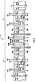
- the sense circuit is designated by the general reference character 100 , and includes a left memory cell array 102 having a pair of left bit lines ( 104 a and 104 b), and right memory cell array 106 having a pair of right bit lines ( 108 a and 108 b).
- the bit line pairs ( 104 a/b and 108 a/b) are coupled to a pair of sense nodes ( 110 and 112 ) by left and right transfer gates ( 114 and 116 ).
- a sense amplifier 118 Disposed between the sense nodes ( 110 and 112 ) is a sense amplifier 118 , a local input/output (I/O) line circuit 120 , and a precharge and equalization circuit 122 .
- the sense circuit enters an active mode by a control signal /RAS (a "row address strobe" signal) transitioning from a high to low voltage at time t0.
- a control signal /RAS a "row address strobe" signal
- the signal EQ is, and has been previously, at a high level. Consequently, the n-channel MOS transistors in the precharge and equalization circuit 122 are all turned on, and both the sense nodes 110 are shorted together and brought to a reference voltage, shown as Vref.
- the EQ signal falls from a high to a low voltage level. This turns the precharge and equalization circuit 122 off.
- the sense nodes ( 110 and 112 ) are thus isolated and precharged at the Vref potential.
- one of the signals CPGL or CPGR falls low while the other remains high, isolating one pair of bit lines to the sense nodes ( 110 and 112 ) and maintaining the other pair of bit lines coupled to the sense nodes ( 110 and 112 ).
- transfer gate 114 is remains enabled by the signal CPGL staying high and CPGR going low.
- the bit lines ( 104 a/b and 108 a/b) remain precharged at the Vref potential.
- a word line is driven high, coupling a memory cell to a bit line.
- the left memory cell array 102 is shown to include word lines, WL0L and WL1L
- the right memory cell array 104 is shown to include word lines WL0R and WL1R.
- word line WL0L is driven high.
- Transistor N100 is turned on, and capacitor C100 is coupled to bit line 104 a.
- both bit lines ( 104 a and 104 b) were previously precharged to Vref.
- bit line 104 a when capacitor C100 is coupled to bit line 104 a, the potential of bit line 104 a will vary from the Vref potential while bit line 104 b would remain at Vref. It is assumed that capacitor C100 had a logic "1" value stored within (it was charged to a high voltage), and so bit line 104 a would rise above the Vref potential.
- bit line 104 a is coupled to sense node 110 and bit line 104 b is coupled to sense node 112 , and the difference in the amount of charge on bit lines 104 a and 104 b, created by the activation of the word line, is shared with the sense nodes 110 and 112 , respectively. As a result, sense node 110 rises to a higher potential than sense node 112 .
- the sense amplifier 118 is activated, and the sense nodes ( 110 and 112 ) are driven to opposite power supply voltage levels according to the differential voltage between the sense nodes ( 110 and 112 ).
- the sense amplifier 118 is activated by two complementary signals, SAN and SAP.
- sense node 110 was at a getter potential than sense node 112
- sense node 110 is driven to high voltage and sense node 112 is driven to a low voltage.
- the potential of a bit line is changed by memory cell data to a potential that is either higher than, or lower than a reference voltage.
- the difference between the reference voltage and the bit line is amplified to generated a data signal.
- the strong data signal on the sense nodes ( 110 and 112 ) is coupled to local I/O (LIO) lines, by operation of the LIO circuit 120 .
- the YSEL signal goes high, and sense nodes ( 110 and 112 ) are each coupled to a different LIO line.
- the data on the LIO lines can be subsequently amplified and output.
- the /RAS signal returns high.
- the word line WL0L returns low, isolating capacitor C100 from bit line 104 a.
- the EQ signal goes high, precharging the sense nodes ( 110 and 112 ) to the Vref voltage. It is noted that, the CGPL signal remains high, and so the bit line pair ( 104 a and 104 b) are slow precharged to the Vref voltage.
- the CPGR signal returns high.
- FIGS. 3a and 3b illustrate a prior binary storage scheme for DRAM memory cells.
- FIG. 3a illustrates the storage of a binary 1
- FIG. 3b illustrates the storage of a binary 0.
- the voltage VCC is the high power supply voltage
- the voltage VSS is the low power supply voltage (zero volts).
- the memory cell includes an n-channel MOS transistor N300 and storage capacitor C300.
- the storage capacitor C300 has a storage node 300 at the potential VCC and a plate node 302 at a potential 1 ⁇ 2VCC.
- the storage node 300 is at the low power supply potential VSS and the plate node is at the same 1 ⁇ 2VCC potential.
- a very different approach to increasing memory device density involves abandoning the conventional binary storage approach, and instead, utilizing memory cells that can store more than one state.
- a drawback to such multi-state devices is that they often require manufacturing processes having specialized steps, and therefore are not always easily or reliably implemented.
- a DRAM memory device includes standard memory cells which can store three different states.
- a storage capacitor from a standard memory cell is coupled to a common sense node, to create a potential variation thereon.
- the common sense node is formed by coupling a first sense node to a second sense node. Once a potential variation is generated on the common sense node, the first and second sense nodes are isolated from one another. Depending upon the state of the memory cell, the first and second sense nodes will be at a data high potential, a data intermediate potential, or a data low potential.
- the first sense node is driven to a high or low logic level by a first sense amplifier, which compares the voltage on the first sense node with a first reference voltage.
- the first reference voltage is greater than the data intermediate potential, but less than the data high potential.
- the second sense node is driven to a high or low logic level by a second sense amplifier, which compares the voltage on the second sense node with a second reference voltage.
- the second reference voltage is less than the data intermediate potential, but greater than the data low potential.
- the first and second reference voltages are provided on first and second reference nodes by first and second dummy memory cells.
- the first and second dummy memory cells have storage capacitors that are coupled to the first and second reference nodes, respectively.
- the charge on the first dummy memory cell capacitor is selected so that the first reference voltage will be midway between the data high potential and the data intermediate potential.
- the charge on the second dummy memory cell is selected so that the second reference voltage will be midway between the data intermediate potential and the data low potential.
- the storage capacitors of the dummy memory cells are equivalent in size to the storage capacitors of the standard memory cells. Predetermined voltages less than the power supply voltages are used to charge the storage capacitors of the dummy memory cells.
- the storage capacitors of the dummy memory cells are smaller than storage capacitors of the standard memory cells. Potentials equivalent to the supply voltage are used to charge the storage capacitors of the dummy memory cells.
- bit lines from one of two different memory cell arrays may be coupled to the first and second sense nodes by two sets of transfer gates.
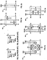
- FIG. 4 a schematic diagram is set forth illustrating a sense circuit for a DRAM which stores data in a ternary form.
- the sense circuit is designated by the general reference character 400 and can be conceptualized as having a left side 402 and a right side 404 joined by an equalization circuit 406 .
- the left and right sides ( 402 and 404 ) of the preferred embodiment 400 have the same general elements. Accordingly, like elements on both sides will be referred to by the same reference character numeral, with the elements on the left side 402 ending with the letter "a", and elements on the right side 404 ending with the letter "b.”
- Each side ( 402 and 404 ) includes an array of DRAM memory cells ( 408 a and 408 b) which provides a first bit line ( 410 a and 410 b) and a second bit line ( 412 a and 412 b).
- a transfer gate ( 414 a and 414 b) couples the first bit line ( 410 a and 410 b) to a first sense node ( 416 a and 416 b), and the second bit line ( 412 a and 412 b) to a second sense node ( 418 a and 418 b).
- Three circuits are coupled between the first ( 416 a and 416 b) and second sense nodes ( 418 a and 418 b): a local input/output (LIO) circuit ( 420 a and 420 b), a reference voltage circuit ( 422 a and 422 b), and a sense amplifier ( 424 a and 424 b).
- the first sense nodes ( 416 a and 416 b) and second sense nodes ( 418 a and 418 b) are coupled to the equalization circuit 406 by internal gates ( 426 a and 426 b).
- FIGS. 5a-5e Detailed schematic diagrams for some of the circuits included within the preferred embodiment 400 are set forth in FIGS. 5a-5e.
- FIG. 5a sets forth a portion of a memory array 408 .
- the memory array 408 includes memory cells M400 and M402 which store data in three states, instead of in a binary form. In response to address signals, the memory array 408 generates a ternary data signal on a bit line.
- the even word line WLA couples a memory cell M400 to the first bit line 410 .
- the odd word line WLB couples memory cell M402 to the second bit line 412 .
- a memory cell when an even word line is activated, a memory cell is coupled to a first bit line 410 while the odd word line remains at a precharge voltage, or vice versa. In this manner, the one bit line of a bit line pair provides a data signal, while the other bit line provides a precharge signal.
- bit lines ( 410 a and 410 b) can be considered “even” bit lines.
- bit lines ( 412 a and 412 b) can be considered “odd” bit lines.
- the first sense nodes ( 416 a and 416 b) can also be considered “even” sense nodes, as the activation of an even word line will place ternary data signals on the first sense nodes ( 416 a and 416 b).
- the second sense nodes ( 418 a and 418 b) can be considered “odd” sense nodes.
- the odd sense nodes ( 418 a and 418 b) will provide reference voltages. Conversely, if an odd word line is activated, the even sense nodes ( 416 a and 416 b) will provide reference voltages.
- first and second sense amplifiers 424 a and 424 b
- memory arrays 408 a and 408 b
- an alternate arrangement could include the first and second sense amplifiers ( 424 a and 424 b) being at opposite ends of one array.
- FIG. 5b illustrates a transfer gate 414 .
- the transfer gate 414 couples the first and second bit lines ( 410 and 412 ) to a first a second sense node ( 416 and 418 ) to provide the ternary data signals to the sense amplifier 424 .
- the transfer gate 414 is shown to include two n-channel MOS transistors in parallel. The gate of both transistors receive an SHRR/L signal. The last letter of the signal identification indicates that there is a "left" side signal and a "right” side signal. Accordingly, the left transfer gated 414 a of FIG. 4 is activated by an SHRL signal, and the right transfer gate 414 b is activated by a SHRR signal.
- the SHRL/R signals may be "booted" signals. That is, when high, the signals that may exceed the maximum power supply voltage in order to eliminate the introduction of a threshold voltage drop between the bit lines ( 410 and 412 ) and sense nodes ( 416 and 418 ).
- FIG. 5c illustrates a sense amplifier 424 .
- two sense amplifiers 424 a and 424 b are utilized.
- One sense amplifier 424 a drives its sense nodes ( 416 a and 418 a) to opposite voltages in response to the differential voltage created by a ternary data signal on one sense node, and a first reference voltage on the other sense node.
- the other sense amplifier 424 b drives its sense nodes ( 416 b and 418 b) to opposite voltages in response to the differential voltage created by a ternary data signal on one of its sense nodes, and a second reference voltage on the other sense node.
- the sense amplifier is a CMOS sense amplifier having a first CMOS driver, formed from p-channel MOS transistor P400 and n-channel MOS transistor N400, cross-coupled to a second CMOS driver, formed from p-channel MOS transistor P402 and n-channel MOS transistor N402.
- the sources of transistors P400 and P402 are coupled to a high sense amplifier supply voltage, shown as SDP, by p-channel MOS transistor P404.
- the gate of transistor P404 is driven by a sense amplifier enable signal SAPS.
- the sources of transistors N400 and N402 are coupled to a low sense amplifier supply voltage, shown as SDN, by n-channel MOS transistor N404.
- the gate of transistor N404 is driven by sense amplifier enable signal SANS.
- SANS sense amplifier enable signal
- the sense amplifier 424 circuit When enabled by a low SAPS signal and a high SANS signal, the sense amplifier 424 circuit will couple one of the sense nodes ( 416 or 418 ) to the SDP voltage, and the other sense node ( 418 or 416 ) to the SDN voltage.
- FIG. 5d sets forth an LIO circuit 420 .
- the LIO circuit 420 is used to couple the data on a pair of sense nodes ( 416 and 418 ) to a pair of LIO lines 428 . In the preferred embodiment set forth in FIG. 4, it is the combination of the data on the left side LIO lines 428 a and the right side LIO lines 428 b that present binary signals in response to a ternary data signal.
- the LIO circuit 420 includes a first n-channel MOS transistor N406 for coupling tile first sense node 416 to one LIO line, and a second n-channel MOS transistor N408 for coupling the second sense node 418 to the other LIO line. The gates of transistors N406 and N408 are both driven by a YSEL signal.
- FIG. 5e sets forth the equalization circuit 406 in a schematic diagram.
- the equalization circuit 406 functions in conjunction with the internal gates ( 426 a and 426 b) and transfer gates ( 414 a and 414 b) to precharge the sense nodes ( 416 a/b, 418 a/b) and bit lines ( 410 a/b and 412 a/b) to a precharge voltage, VBLR.
- the equalization circuit 406 is disposed between equalization nodes 430 and 432 , and is shown to include an n-channel MOS shorting transistor N410, and two n-channel MOS precharge transistors N412 and N414.
- the gates of transistors N410, N412 and N414 are commonly driven by an EQ signal.
- the equalization circuit 406 When the equalization circuit 406 is activated by a high EQ signal, the shorting transistor N410 shorts the equalization nodes ( 430 and 432 ) together, and the precharge transistors (N412 and N414) provide the precharge voltage VBLR to the equalization nodes ( 430 and 432 ).
- the precharge voltage VBLR is midway between the supply voltages, VCC and VSS.
- the combination of the inner gates ( 426 a and 426 b) and equalization nodes ( 430 and 432 ) can be considered together as an inner gate circuit that functions to couple the left side pair of sense nodes ( 416 a and 418 a) to the right side pair of sense nodes ( 416 b and 418 b.
- both reference circuits ( 422 a and 422 b) and internal gates ( 426 a and 426 b) are shown in detail.
- both reference circuits ( 422 a and 422 b) employ dummy cells to generate a reference voltage.
- the first reference voltage circuit 422 a is shown to include two dummy memory cells.
- the first dummy memory cell includes pass transistor N416a and storage capacitor C400a.
- the second dummy memory cell includes pass transistor N418a and storage capacitor C402a.
- the first dummy memory cell is coupled to the second sense node 418 a by even dummy word line signal DWLA.
- DWLA is high whenever an even word line, in either memory cell array 408 a or 408 b, is driven high.
- the second dummy memory cell is coupled to the first sense node 416 a by odd dummy word line signal DLWB whenever an odd word line, in either memory cell array 408 a or 408 b, is drive high.
- Storage capacitors C400a and C402a have a common storage node 434 a that is coupled to a first reference charge potential DCRH by an n-channel MOS dummy precharge transistor N420a.
- the opposing nodes of capacitors C400a and C402a are coupled to a plate node.
- the gate of transistor N420a is driven by a dummy precharge signal DPC.
- the second reference voltage circuit 422 b has the same general configuration as the first reference voltage circuit 422 a: a first dummy memory cell (N416b and C400b), a second dummy memory cell (N418b and C402b), and a dummy precharge transistor N420b for coupling storage nodes of the capacitors C400b and C402b to a second reference charge potential DCRL.
- the difference between the first and second reference voltage circuits 422 a and 422 b is the magnitude of the reference charge potentials (DCRH and DCRL). The magnitude of the two reference charge potentials (DCRH and DCRL) will be discussed below.
- FIG. 4 illustrates a dummy capacitor pair (C400a/C402a and C400b/C402b) within each reference voltage circuit ( 422 a and 422 b) each pair could be replaced by a single capacitor.
- the memory cell is designated by the general reference character 600 , and includes a pass transistor N600 and storage capacitor C600.
- the storage capacitor has a storage node 602 and a plate node 604 .
- the plate node 604 is maintained at plate voltage of 1 ⁇ 2VCC, where VCC is the high power supply, and VSS is the low power supply (zero volts).
- FIG. 6a shows the voltage levels for a logic "0" value, in which the storage node 602 is charged to the low power supply voltage VSS.
- FIG. 6b shows the voltage levels for a logic "1” value, in which the storage node 602 is charged to a 1 ⁇ 2VCC voltage level.
- FIG. 6c shows the voltage levels for a logic "2" value, in which the storage node is charged to the high power supply voltage VCC.
- the plate nodes of the memory cells the same array are commonly connected.
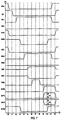
- FIG. 7 is a timing diagram illustrating the response of various signals used in the operation of the preferred embodiment 400 .
- FIG. 8a is a timing diagram illustrating the response of the first sense node 416 a and first reference node 418 a for the various possible read-write logic operations that may occur in the operation of the preferred embodiment.
- FIG. 8b is a timing diagram which illustrates the response of the second sense node 416 b and second reference node 418 b for same combinations of read-write operations set forth in FIG. 8a.
- the preferred embodiment 400 Prior to time t0, the preferred embodiment 400 is in the stand-by state. In this state the bit lines, sense nodes and equalization nodes are all precharged to the voltage 1 ⁇ 2VCC. Referring now to FIGS. 4 and 5a-5e in conjunction with FIG. 7, it is shown that prior to time t0, the signal EQ is high, and so the equalization circuit 406 is active.
- the word lines (represented by the even and odd word lines WLA and WLB) are all low, isolating the memory cell storage capacitors from the bit lines ( 410 a/b and 412 a/b).
- the dummy word lines are also low, isolating the dummy memory cells from the sense nodes ( 416 a/b and 418 a/b).
- the SHRL, SHRR and SHRM signals are all high, enabling both the left and right transfer gates ( 414 a), as well as the internal gates ( 426 a and 426 b).
- the first bit lines ( 410 a and 410 b), the first sense nodes ( 416 a and 416 b), and equalization node 430 are shorted together.
- the second bit lines ( 412 a and 412 b), the second sense nodes ( 418 a and 418 b), and the equalization node 432 are shorted together. Because the equalization circuit 406 is active, all of the above bit lines ( 410 a/b and 412 a/b), sense nodes ( 416 a/b and 418 a/b), and equalization nodes ( 430 and 432 ) are brought to the precharge voltage VBLR, which in the preferred embodiment is 1 ⁇ 2VCC.
- the sense amplifiers ( 424 a and 424 b) are disabled by the levels of their high and low supply voltages (SDP and SDN). As shown in FIG. 7, while the sense amplifier enable signals (SANS and SAPS) are active, the sense amplifier high and low supply voltages (SDP and SDN) are both at the 1 ⁇ 2VCC voltage. Because the sense nodes are also at the 1 ⁇ 2VCC voltage level, the sense amplifiers ( 424 a and 424 b) are disabled.
- the stand-by state also serves to charge the dummy memory cell capacitors (C400a/b) and C402a/b).
- the DPC signal Prior to time t0, the DPC signal is high, and the common storage node 434 a in the first reference voltage circuit 422 a is coupled to the first reference charge potential DCRH, and the common storage node 434 b in the second reference voltage circuit 422 b is coupled to the second reference charge potential DCRL.
- the LIO circuits 420 a and 420 b Prior to time t0, the LIO circuits 420 a and 420 b are disabled, and the LIO lines 428 a and 428 b are isolated from the sense nodes ( 416 a/b and 418 a/b).
- a rewrite timing signal SASE is also inactive (low). The SASE signal will be described in more detail below.
- a row address strobe timing signal /RAS falls from a logic high to a logic low state. This transition may be the result of an externally applied /RAS signal, in the case of an asynchronous DRAM, or may be the result of an external clock signal, in the case of a synchronous DRAM.
- data is accessed from the right memory cell array 408 b. Accordingly, at about time t0, the signal SHRL goes low, disabling transfer gate 414 a, and isolating the left memory cell array 408 a from the rest of the preferred embodiment 400 .
- the SHRR signal remains high, and so bit line 410 b remains coupled to the first sense nodes ( 416 a and 416 b) and equalization node 430 , and bit line 412 a remains coupled to the second sense nodes ( 418 a and 418 b) and equalization node 432 .
- the DPC signal transitions from a high voltage to a low voltage.
- transistor N420a in the first reference voltage circuit 422 a, and transistor N420b in the second reference voltage circuit 422 b, are turned off. It is noted that capacitors C400a and C402a are charged to the DCRH voltage, and capacitors C400b and C402b are charged to the DCRL voltage.
- the equalization function is terminated as the EQ signal falls from a high to a low voltage.
- transistors N410, N412 and N414 are turned off, and equalization node 430 is isolated from equalization node 432 .
- ternary memory cell data is coupled to one bit line of a bit line pair.
- Word line WLA transitions from a low voltage to a high voltage.
- word line WLA represents an even word line in the memory cell arrays ( 408 a and 408 b).
- a memory cell (for example memory cell M400) is coupled to the first bit lines 410 b.
- the left transfer gate 414 a is inactive while the right transfer gate 414 b remains active, consequently, ternary cell data on bit line 410 b is coupled to the first sense nodes ( 416 a and 416 b) and equalization node 430 .
- the second sense nodes ( 418 a and 418 b) and equalization node 432 remain at the precharge voltage 1 ⁇ 2VCC.
- a ternary data signal is coupled to a common sense node formed by the first sense nodes ( 416 a and 416 b) being coupled together by transfer gates ( 426 a and 426 b).
- Waveform 800 a illustrates the response of the first and second sense nodes ( 416 a and 418 a) of the preferred embodiment 400
- waveform 800 b illustrates the response of the first and second sense nodes ( 416 b and 418 b) of the preferred embodiment 400 .
- waveforms 800 a and 800 b it is shown that at time t2. when the memory cell storage capacitor (charged to the ternary value of VCC) is coupled to bit line 410 b by word line WLA going high, the first sense nodes ( 416 a and 418 a) begin to rise in potential above their respective second sense nodes ( 418 a and 418 b), which remain at the precharge potential 1 ⁇ 2VCC.
- the magnitude of the voltage differential is shown in FIGS. 8a and 8b as the voltage Vsense .
- the magnitude of Vsense is given the equation below.
- Vsense VCC 2 Ccell Csa + Cbl + Ccell
- the VCC/2 term represents the voltage on the storage capacitor for a ternary 2 or ternary 0 value (i.e., VCC-1 ⁇ 2VCC or 1 ⁇ 2VCC-VSS).
- the term Ccell is the capacitance of the memory cell
- the term Csa is the capacitance of the sense amplifier (i.e., a left and a right sense node)
- Cbl is the capacitance of a bit line.
- the left pair of sense nodes ( 416 a and 418 b) and the right pair of sense nodes ( 416 b and 418 b) are isolated, trapping the voltage differential created by ternary cell data on the bit line 410 b.
- the signal SHRR goes low, turning off the right transfer gate 414 b, isolating the sense nodes ( 416 a/b and 418 a/b) from bit lines 410 b and 412 b.
- the signal SHRM also goes low, turning off internal gates 426 a and 426 b, isolating the sense nodes ( 416 a/b and 418 a/b) from the equalization nodes ( 430 and 432 ). In this manner the two sense nodes forming the common sense node are isolated from one another.
- dummy word lines are activated, creating a first reference voltage on the one of the left sense nodes ( 416 a or 418 a) and a second reference voltage on one of the right sense nodes ( 416 b or 418 b).
- the second sense node 418 a on the left side 402 of the preferred embodiment is driven to a first reference voltage
- the second sense node 418 b on the right side 404 is driven to a second reference voltage.
- dummy word line DWLA is activated to couple a dummy memory cell to the second sense nodes ( 418 a and 418 b). It is understood that had an odd word line been activated (for example word line WLB in FIG. 5a), dummy word line DWLB would be activated at this time period, while dummy word line DWLA would remain low.
- the first sense nodes ( 416 a and 416 b) serve as "sense" nodes in that they receive ternary data signals, while the second sense nodes ( 418 a and 418 b) function as reference nodes in that they provide different reference voltages.
- the second sense nodes ( 418 a and 418 b) serve as the sense nodes, while the first sense nodes ( 416 a and 416 b) serve as the reference nodes.
- Vref 1 VCC 2 + DCRH Ccell Csa 2 + Ccell
- the voltage on the dummy word line capacitors (C400b and C402b) on the opposing side of the preferred embodiment 400 is selected so as to drive the second sense node 418 a to a second reference voltage VCC/2-Vref2 .
- the second sense node 418 b falls below the 1 ⁇ 2VCC level.
- the sense amplifiers ( 424 a and 424 b) are activated, and the sense node pairs ( 416 a/ 418 a and 416 b/ 418 b) are driven to opposite supply voltage levels according to the differential voltage between them.
- the sense amplifier high supply voltage SDP rises from 1 ⁇ 2VCC to a full VCC level.
- the sense amplifier low supply voltage SDN falls from 1 ⁇ 2VCC to VSS (zero volts).
- waveform 800 a of FIG. 8a prior to time t5, the potential of the first sense node 416 a is higher than the potential of the second sense node 418 a.
- the first sense node 416 a is driven to the VCC potential and the second sense node 418 a is driven to the VSS potential.
- the response of the other sense node pairs is shown in waveform 800 b of FIG. 8b.
- the first node 416 b is driven to the VCC potential and the second node 418 b is driven to the VSS potential.
- the data on the sense node pairs ( 416 a/ 418 a and 416 b/ 418 b) is coupled to the LIO lines ( 428 a and 428 b) by operation of the LIO circuits ( 420 a and 420 b).
- the YSEL signal rises from a low to high voltage.
- the high YSEL signal turns on transistors N406 and N408 coupling sense nodes 416 and 418 to LIO line pair 428 .
- the YSEL signal remains high to account for a write operation.
- the example of FIG. 7 sets forth a case where no write operation takes place, or alternately, the same data value (ternary 2) is to be written back into the memory cell. Accordingly, there is no transition in voltage at time t7. Examples of read-write operations in which such a transition may occur at time t7 will be described in more detail below.
- the YSEL signal returns to a low voltage, disabling the LIO circuits ( 420 a and 420 b) and isolating the LIO lines ( 428 a and 428 b) from the sense node pairs ( 416 a/ 418 a and 416 b/ 418 b).
- a rewrite operation is initiated to drive the sense node pairs ( 416 a/ 418 a and 416 b/ 418 b) to opposite supply voltage levels, in order to write data back into the memory array ( 408 a and 408 b).
- the data write may occur in the write portion of a read/write operation, or to refresh the data stored within the memory arrays ( 408 a and 408 b).
- an SASE signal goes high.
- the SASE signal is provided to either enable or disable the sense amplifiers ( 424 a and 424 b), depending upon the voltages at the sense node pairs ( 416 a/ 418 a and 416 b/ 418 b). In the event the sense node pairs have ( 416 a/ 418 a and 416 b/ 418 b) the same voltage levels, the sense amplifiers ( 424 a and 424 b) will remain enabled, and the SAPS signal will remain low, and the SANS signal will remain high.
- the sense amplifiers ( 424 a and 424 b) will be disabled, to prevent the sense amplifiers ( 424 a and 424 b) from fighting each other during the write operation, and hence drawing excessive amounts of current.
- the signal SAPS will thus go high, and the SANS signal will go low, as long as SASE signal is high.
- FIG. 9 illustrates a timing control circuit for generating the sense amplifier enable signals, SANS and SAPS set forth in FIG. 7.
- the timing control circuit is designated by the reference character 900 and is shown to include a three input NAND gate G900.
- One input to gate G900 is the voltage level at the first sense node 416 a.
- a second input is the inverse of the voltage level at the second sense node 416 b.
- the third input to gate G900 is the SASE signal.
- the output of gate G900 is the SANS signal.
- the SAPS signal is the inverse of the SANS signal.
- the first nodes ( 416 a and 416 b) are both at VCC at time t9. Accordingly, the SAPS signal will remain low, and the SANS signal will remain high.
- ternary data is written back into the memory cell arrays.
- the SHRM signal returns high, enabling internal gates ( 426 a and 426 b).
- the first nodes 416 a and 416 b are coupled together by way of equalization node 430
- the second nodes 418 a and 418 b are coupled together by way of equalization node 432 . It is recalled that if the voltage levels of the two sense node pairs ( 416 a/ 418 a and 416 b/ 418 b) were equal (i.e., both at VCC or both at VSS), the sense amplifiers ( 424 a and 424 b) would remain enabled, and would operate together in the write function.
- the sense amplifiers ( 424 a and 424 b) would be disabled, and the activation of the internal gates ( 426 a and 426 b) would short the oppositely charge sensed node pairs ( 416 a/ 418 a and 416 b/ 418 b) resulting in both nodes ending up at the 1 ⁇ 2VCC voltage level.
- the equalization circuit 406 may also become active, earlier in this case, to drive the sense nodes pairs ( 416 a/ 418 a and 416 b/ 418 b) to the 1 ⁇ 2VCC voltage level.
- the signal SHRR returns high, enabling the right side transfer gate 414 b, coupling bit line 410 b to the first sense nodes ( 416 a and 416 b), and bit line 412 b to the second sense nodes ( 418 a and 418 b). Because word line WLA is still at a high voltage, data will be written back into the memory cell storage capacitor.
- the active cycle begins to conclude.
- the timing signal /RAS returns to a high voltage
- word line WLA returns to a low voltage.
- the corresponding dummy word line DWLA also returns to a low voltage. In this way, the storage capacitors of the standard and dummy memory cells are disconnected from the bit lines and sense nodes.
- the preferred embodiment is returned to the stand-by state by an equalization operation.
- the EQ signal goes high, and the first and second sense nodes ( 416 a/b and 418 a/b) are precharged and equalized to the 1 ⁇ 2VCC level.
- the SHRL signal returns high, enabling the left transfer gate 414 a. Because both the left and right transfer gates ( 414 a and 414 b) are enabled at this time, the bit lines ( 410 a/b and 412 a/b) are also precharged and equalized to the 1 ⁇ 2VCC voltage level.
- the sense amplifiers ( 424 a and 424 b) are disabled, and the dummy memory cells within the reference voltage circuits ( 422 a and 422 b) are precharged.
- the SASE signal returns low, and the SDP and SDN supply voltages return to the 1 ⁇ 2VCC level.
- the DPC signal goes high, and the common storage nodes 434 a is precharged to the DCRH voltage, while the common storage node 434 b is precharged to the DCRL voltage.
- Each of the waveforms in FIG. 8a represent the response of the left side sense nodes ( 416 a and 418 a) to a different read/write operation.
- FIG. 8b illustrates the response of the right side sense nodes ( 416 b and 418 b) to the same read/write operations of FIG. 8a.
- Waveforms 800 a/b, 802 a/b and 804 a/b set forth an operation that begins with the read of a ternary 2 data signal. Accordingly, the waveforms are generally the same from time t0 to time t7.
- the read ternary 2/write ternary 2 operation shown by waveforms 800 a and 800 b has already been described.
- a read ternary 2/write ternary 1 operation is shown by waveforms 802 a and 802 b. Accordingly, the waveform 802 a differs from waveform 800 a, in that at time t7 the LIO lines 428 a are driven to opposite voltage levels, reversing the differential potential at the sense nodes ( 416 a and 416 b), and causing the sense amplifier 424 a to flip. The voltage at the sense nodes 416 a and 418 a are thus driven to opposite level at time t7.
- the sense amplifiers ( 424 a and 424 b) are disabled and the activation of internal gates ( 426 a and 426 b) result in the sense nodes ( 416 a/b and 418 a/g) being equalized to the 1 ⁇ 2VCC voltage level.
- Waveforms 804 a and 804 b illustrate a read ternary 2/write ternary 0 operation.
- both LIO line pairs 428 a and 428 b are driven to flip both sense amplifiers 424 a and 424 b. Accordingly, at time t7, the sense node voltages for the both left and right sides of the preferred embodiment 400 are reversed.
- Waveforms 806 a/b, 808 a/b and 810 a/b illustrate three operations that begin with a read ternary 1 operation.
- Waveforms 812 a/b, 814 a/b and 816 a/b illustrate three operations that begin with a read ternary 0 operation.
- the functioning of the preferred embodiment 400 for these operations would be clear to one skilled in the art, in light of the description above.
- the left transfer gate 414 a can be considered a first data passing gate which couples the data from a bit line to a first sense node 416 a.
- the combination of the inner gates ( 426 a and 426 b) can be considered a second data passing gate which couples the data signals from the bit line to a second sense node 416 b.
- These first and second data passing gates ( 414 a and 426 a/b) are subsequently turned off, isolating the first sense node 416 a from the second sense node 416 b.
- the potential on the two sense nodes ( 416 a and 416 b) are then driven by two different sense amplifiers ( 424 a and 424 b) which drive the sense nodes ( 416 a and 416 b) by comparing the potential thereof with two different reference voltages (Vref1 and Vref2).
- sense nodes 418 a and 418 b would be considered the first and second sense nodes.
- the right transfer gate 414 b would be considered the first data passing gate, with the combination of inner gates ( 426 a and 426 b) functioning again as the second data transfer gates.
- FIG. 10 a table is set forth to more clearly illustrate the relationship between LIO line voltage levels and ternary cell data, according to a preferred embodiment.
- two of the ternary states (0 and 2) result in both pairs of LIO lines ( 428 a and 428 b) being driven to the same logic state.
- the third ternary state (1) results in the LIO line pairs ( 428 a and 428 b) being driven to opposite logic states.
- ternary storage semiconductor memory device can provide increased data density, the semiconductor device must still interact with other devices configured for binary information. Thus, it is desirable to convert ternary information into binary information.
- FIG. 11 illustrates a conversion scheme for translating ternary information to binary information.
- two ternary data cells are used to generate the equivalent of three binary data cells.
- two, three-state bits are translated into three, two-state bits.
- the ternary cell data "22" is not used. It is understood that a different data set could be selected as the non-used combination.
- the preferred embodiment 400 utilizes two sense amplifiers to sense ternary data. Such an arrangement departs from conventional binary DRAM arrangements in that a pair of sense amplifiers (as opposed to just one sense amplifier) must be coupled to each bit line. This constraint may give rise to difficulties in the physical placement of the components of the preferred embodiment 400 in an integrated circuit layout.
- FIG. 12 represents an approach for laying out the preferred embodiment 400 in a semiconductor substrate.
- the layout approach is designated by the general reference character 1200 , and shows the placement of four sense circuits, designated by the reference characters 1202 a- 1202 d. It is understood that each of the circuits ( 1202 a- 1202 d) includes two sense amplifier circuits, two LIO circuits, two reference circuits, two transfer gates, and one equalization circuit. To assist in the understanding of the layout, only the two sense amplifiers (designated by reference characters 1204 a and 1204 b) are shown in each of the circuits ( 1202 a- 1202 d).
- the layout 1200 emphasizes the interchangeability of the terms "right” and "left” as used in the description of the preferred embodiment 400 .
- a memory cell array 1206 is shown situated between circuits 1202 a and 1202 c, and between circuits 1202 b and 1202 d.
- the memory array 1206 could serve as the "right" memory cell array for circuit 1202 a and the "left” memory cell array for circuit 1202 c.
Landscapes
- Engineering & Computer Science (AREA)
- Computer Hardware Design (AREA)
- Microelectronics & Electronic Packaging (AREA)
- Dram (AREA)
- Read Only Memory (AREA)
Applications Claiming Priority (2)
| Application Number | Priority Date | Filing Date | Title |
|---|---|---|---|
| US6717897P | 1997-12-01 | 1997-12-01 | |
| US67178P | 1997-12-01 |
Publications (2)
| Publication Number | Publication Date |
|---|---|
| EP0920029A2 true EP0920029A2 (de) | 1999-06-02 |
| EP0920029A3 EP0920029A3 (de) | 1999-07-14 |
Family
ID=22074226
Family Applications (1)
| Application Number | Title | Priority Date | Filing Date |
|---|---|---|---|
| EP98309784A Withdrawn EP0920029A3 (de) | 1997-12-01 | 1998-11-30 | RAM-Speicher mit mehreren Zuständen |
Country Status (4)
| Country | Link |
|---|---|
| EP (1) | EP0920029A3 (de) |
| JP (1) | JPH11238385A (de) |
| KR (1) | KR19990062662A (de) |
| TW (1) | TW418527B (de) |
Cited By (2)
| Publication number | Priority date | Publication date | Assignee | Title |
|---|---|---|---|---|
| CN115376600A (zh) * | 2022-08-26 | 2022-11-22 | 长鑫存储技术有限公司 | 存储器的测试方法、装置、设备及介质 |
| US11811424B2 (en) | 2021-04-05 | 2023-11-07 | Micron Technology, Inc. | Fixed weight codewords for ternary memory cells |
Families Citing this family (1)
| Publication number | Priority date | Publication date | Assignee | Title |
|---|---|---|---|---|
| KR20030003312A (ko) * | 2001-06-30 | 2003-01-10 | 주식회사 하이닉스반도체 | 다중 비트 커패시터를 갖는 반도체 메모리 |
Family Cites Families (2)
| Publication number | Priority date | Publication date | Assignee | Title |
|---|---|---|---|---|
| US5532955A (en) * | 1994-12-30 | 1996-07-02 | Mosaid Technologies Incorporated | Method of multilevel dram sense and restore |
| US5684736A (en) * | 1996-06-17 | 1997-11-04 | Nuram Technology, Inc. | Multilevel memory cell sense amplifier system |
-
1998
- 1998-11-30 KR KR1019980052076A patent/KR19990062662A/ko not_active Withdrawn
- 1998-11-30 EP EP98309784A patent/EP0920029A3/de not_active Withdrawn
- 1998-12-01 JP JP10342052A patent/JPH11238385A/ja active Pending
- 1998-12-24 TW TW087119841A patent/TW418527B/zh not_active IP Right Cessation
Cited By (2)
| Publication number | Priority date | Publication date | Assignee | Title |
|---|---|---|---|---|
| US11811424B2 (en) | 2021-04-05 | 2023-11-07 | Micron Technology, Inc. | Fixed weight codewords for ternary memory cells |
| CN115376600A (zh) * | 2022-08-26 | 2022-11-22 | 长鑫存储技术有限公司 | 存储器的测试方法、装置、设备及介质 |
Also Published As
| Publication number | Publication date |
|---|---|
| EP0920029A3 (de) | 1999-07-14 |
| KR19990062662A (ko) | 1999-07-26 |
| TW418527B (en) | 2001-01-11 |
| JPH11238385A (ja) | 1999-08-31 |
Similar Documents
| Publication | Publication Date | Title |
|---|---|---|
| US6724646B2 (en) | Dummy cell structure for 1T1C FeRAM cell array | |
| US8009459B2 (en) | Circuit for high speed dynamic memory | |
| CN1759448B (zh) | 读出放大器、包括其的存储设备、计算机系统和方法 | |
| US8295101B2 (en) | Semiconductor device | |
| CN102956262B (zh) | 静态ram | |
| US5339274A (en) | Variable bitline precharge voltage sensing technique for DRAM structures | |
| US6678198B2 (en) | Pseudo differential sensing method and apparatus for DRAM cell | |
| JPS63149900A (ja) | 半導体メモリ | |
| US7613024B2 (en) | Local digit line architecture and method for memory devices having multi-bit or low capacitance memory cells | |
| JP4118364B2 (ja) | 半導体記憶装置 | |
| US5625588A (en) | Single-ended sensing using global bit lines for DRAM | |
| US4769792A (en) | Semiconductor memory device with voltage bootstrap | |
| US6570799B1 (en) | Precharge and reference voltage technique for dynamic random access memories | |
| US4926381A (en) | Semiconductor memory circuit with sensing arrangement free from malfunction | |
| US5719813A (en) | Cell plate referencing for DRAM sensing | |
| US7036056B2 (en) | Semiconductor memory device having time reduced in testing of memory cell data reading or writing, or testing of sense amplifier performance | |
| US20100008129A1 (en) | Semiconductor memory device and method of controlling the same | |
| EP0920029A2 (de) | RAM-Speicher mit mehreren Zuständen | |
| US6137715A (en) | Static random access memory with rewriting circuit | |
| US6788590B2 (en) | Bitline reference voltage circuit | |
| JPH10334672A (ja) | 半導体記憶装置 | |
| KR100269597B1 (ko) | 반도체 메모리 | |
| US11955170B2 (en) | Low-power static random access memory | |
| JP3182155B2 (ja) | 半導体集積回路 | |
| JPS6325879A (ja) | スタテイツク型半導体メモリ |
Legal Events
| Date | Code | Title | Description |
|---|---|---|---|
| PUAI | Public reference made under article 153(3) epc to a published international application that has entered the european phase |
Free format text: ORIGINAL CODE: 0009012 |
|
| PUAL | Search report despatched |
Free format text: ORIGINAL CODE: 0009013 |
|
| AK | Designated contracting states |
Kind code of ref document: A2 Designated state(s): DE FR GB IT NL |
|
| AX | Request for extension of the european patent |
Free format text: AL;LT;LV;MK;RO;SI |
|
| AK | Designated contracting states |
Kind code of ref document: A3 Designated state(s): AT BE CH CY DE DK ES FI FR GB GR IE IT LI LU MC NL PT SE |
|
| AX | Request for extension of the european patent |
Free format text: AL;LT;LV;MK;RO;SI |
|
| 17P | Request for examination filed |
Effective date: 19991222 |
|
| AKX | Designation fees paid |
Free format text: DE FR GB IT NL |
|
| 17Q | First examination report despatched |
Effective date: 20000818 |
|
| STAA | Information on the status of an ep patent application or granted ep patent |
Free format text: STATUS: THE APPLICATION IS DEEMED TO BE WITHDRAWN |
|
| 18D | Application deemed to be withdrawn |
Effective date: 20010313 |