EP0920097A2 - Dispositif laser à semi-conducteur - Google Patents
Dispositif laser à semi-conducteur Download PDFInfo
- Publication number
- EP0920097A2 EP0920097A2 EP98309626A EP98309626A EP0920097A2 EP 0920097 A2 EP0920097 A2 EP 0920097A2 EP 98309626 A EP98309626 A EP 98309626A EP 98309626 A EP98309626 A EP 98309626A EP 0920097 A2 EP0920097 A2 EP 0920097A2
- Authority
- EP
- European Patent Office
- Prior art keywords
- layer
- layers
- cladding layer
- optical guide
- type cladding
- Prior art date
- Legal status (The legal status is an assumption and is not a legal conclusion. Google has not performed a legal analysis and makes no representation as to the accuracy of the status listed.)
- Granted
Links
- 239000004065 semiconductor Substances 0.000 title claims abstract description 24
- 238000005253 cladding Methods 0.000 claims abstract description 56
- 230000003287 optical effect Effects 0.000 claims abstract description 26
- 230000000903 blocking effect Effects 0.000 claims abstract description 17
- 238000010521 absorption reaction Methods 0.000 abstract description 10
- 230000003247 decreasing effect Effects 0.000 description 8
- 229910000980 Aluminium gallium arsenide Inorganic materials 0.000 description 7
- 229910001218 Gallium arsenide Inorganic materials 0.000 description 5
- 239000000758 substrate Substances 0.000 description 5
- 230000007423 decrease Effects 0.000 description 4
- 239000000203 mixture Substances 0.000 description 4
- 238000006243 chemical reaction Methods 0.000 description 2
- 238000009826 distribution Methods 0.000 description 2
- 238000005468 ion implantation Methods 0.000 description 2
- 230000000630 rising effect Effects 0.000 description 2
- 229910000530 Gallium indium arsenide Inorganic materials 0.000 description 1
- 230000001133 acceleration Effects 0.000 description 1
- 230000004888 barrier function Effects 0.000 description 1
- 239000000969 carrier Substances 0.000 description 1
- 230000015556 catabolic process Effects 0.000 description 1
- 238000005229 chemical vapour deposition Methods 0.000 description 1
- 238000004891 communication Methods 0.000 description 1
- 230000000052 comparative effect Effects 0.000 description 1
- 230000002708 enhancing effect Effects 0.000 description 1
- 238000002347 injection Methods 0.000 description 1
- 239000007924 injection Substances 0.000 description 1
- 230000004807 localization Effects 0.000 description 1
- 238000003754 machining Methods 0.000 description 1
- 239000000463 material Substances 0.000 description 1
- 239000002184 metal Substances 0.000 description 1
- 238000000034 method Methods 0.000 description 1
- 230000010355 oscillation Effects 0.000 description 1
- 230000005855 radiation Effects 0.000 description 1
- 230000006798 recombination Effects 0.000 description 1
- 238000005215 recombination Methods 0.000 description 1
Images

Classifications
-
- H—ELECTRICITY
- H01—ELECTRIC ELEMENTS
- H01S—DEVICES USING THE PROCESS OF LIGHT AMPLIFICATION BY STIMULATED EMISSION OF RADIATION [LASER] TO AMPLIFY OR GENERATE LIGHT; DEVICES USING STIMULATED EMISSION OF ELECTROMAGNETIC RADIATION IN WAVE RANGES OTHER THAN OPTICAL
- H01S3/00—Lasers, i.e. devices using stimulated emission of electromagnetic radiation in the infrared, visible or ultraviolet wave range
- H01S3/09—Processes or apparatus for excitation, e.g. pumping
- H01S3/091—Processes or apparatus for excitation, e.g. pumping using optical pumping
- H01S3/094—Processes or apparatus for excitation, e.g. pumping using optical pumping by coherent light
- H01S3/0941—Processes or apparatus for excitation, e.g. pumping using optical pumping by coherent light of a laser diode
- H01S3/09415—Processes or apparatus for excitation, e.g. pumping using optical pumping by coherent light of a laser diode the pumping beam being parallel to the lasing mode of the pumped medium, e.g. end-pumping
-
- H—ELECTRICITY
- H01—ELECTRIC ELEMENTS
- H01S—DEVICES USING THE PROCESS OF LIGHT AMPLIFICATION BY STIMULATED EMISSION OF RADIATION [LASER] TO AMPLIFY OR GENERATE LIGHT; DEVICES USING STIMULATED EMISSION OF ELECTROMAGNETIC RADIATION IN WAVE RANGES OTHER THAN OPTICAL
- H01S5/00—Semiconductor lasers
- H01S5/20—Structure or shape of the semiconductor body to guide the optical wave ; Confining structures perpendicular to the optical axis, e.g. index or gain guiding, stripe geometry, broad area lasers, gain tailoring, transverse or lateral reflectors, special cladding structures, MQW barrier reflection layers
-
- B—PERFORMING OPERATIONS; TRANSPORTING
- B82—NANOTECHNOLOGY
- B82Y—SPECIFIC USES OR APPLICATIONS OF NANOSTRUCTURES; MEASUREMENT OR ANALYSIS OF NANOSTRUCTURES; MANUFACTURE OR TREATMENT OF NANOSTRUCTURES
- B82Y20/00—Nanooptics, e.g. quantum optics or photonic crystals
-
- H—ELECTRICITY
- H01—ELECTRIC ELEMENTS
- H01S—DEVICES USING THE PROCESS OF LIGHT AMPLIFICATION BY STIMULATED EMISSION OF RADIATION [LASER] TO AMPLIFY OR GENERATE LIGHT; DEVICES USING STIMULATED EMISSION OF ELECTROMAGNETIC RADIATION IN WAVE RANGES OTHER THAN OPTICAL
- H01S5/00—Semiconductor lasers
- H01S5/20—Structure or shape of the semiconductor body to guide the optical wave ; Confining structures perpendicular to the optical axis, e.g. index or gain guiding, stripe geometry, broad area lasers, gain tailoring, transverse or lateral reflectors, special cladding structures, MQW barrier reflection layers
- H01S5/22—Structure or shape of the semiconductor body to guide the optical wave ; Confining structures perpendicular to the optical axis, e.g. index or gain guiding, stripe geometry, broad area lasers, gain tailoring, transverse or lateral reflectors, special cladding structures, MQW barrier reflection layers having a ridge or stripe structure
- H01S5/2202—Structure or shape of the semiconductor body to guide the optical wave ; Confining structures perpendicular to the optical axis, e.g. index or gain guiding, stripe geometry, broad area lasers, gain tailoring, transverse or lateral reflectors, special cladding structures, MQW barrier reflection layers having a ridge or stripe structure by making a groove in the upper laser structure
-
- H—ELECTRICITY
- H01—ELECTRIC ELEMENTS
- H01S—DEVICES USING THE PROCESS OF LIGHT AMPLIFICATION BY STIMULATED EMISSION OF RADIATION [LASER] TO AMPLIFY OR GENERATE LIGHT; DEVICES USING STIMULATED EMISSION OF ELECTROMAGNETIC RADIATION IN WAVE RANGES OTHER THAN OPTICAL
- H01S5/00—Semiconductor lasers
- H01S5/20—Structure or shape of the semiconductor body to guide the optical wave ; Confining structures perpendicular to the optical axis, e.g. index or gain guiding, stripe geometry, broad area lasers, gain tailoring, transverse or lateral reflectors, special cladding structures, MQW barrier reflection layers
- H01S5/22—Structure or shape of the semiconductor body to guide the optical wave ; Confining structures perpendicular to the optical axis, e.g. index or gain guiding, stripe geometry, broad area lasers, gain tailoring, transverse or lateral reflectors, special cladding structures, MQW barrier reflection layers having a ridge or stripe structure
- H01S5/227—Buried mesa structure ; Striped active layer
-
- H—ELECTRICITY
- H01—ELECTRIC ELEMENTS
- H01S—DEVICES USING THE PROCESS OF LIGHT AMPLIFICATION BY STIMULATED EMISSION OF RADIATION [LASER] TO AMPLIFY OR GENERATE LIGHT; DEVICES USING STIMULATED EMISSION OF ELECTROMAGNETIC RADIATION IN WAVE RANGES OTHER THAN OPTICAL
- H01S5/00—Semiconductor lasers
- H01S5/20—Structure or shape of the semiconductor body to guide the optical wave ; Confining structures perpendicular to the optical axis, e.g. index or gain guiding, stripe geometry, broad area lasers, gain tailoring, transverse or lateral reflectors, special cladding structures, MQW barrier reflection layers
- H01S5/2004—Confining in the direction perpendicular to the layer structure
-
- H—ELECTRICITY
- H01—ELECTRIC ELEMENTS
- H01S—DEVICES USING THE PROCESS OF LIGHT AMPLIFICATION BY STIMULATED EMISSION OF RADIATION [LASER] TO AMPLIFY OR GENERATE LIGHT; DEVICES USING STIMULATED EMISSION OF ELECTROMAGNETIC RADIATION IN WAVE RANGES OTHER THAN OPTICAL
- H01S5/00—Semiconductor lasers
- H01S5/30—Structure or shape of the active region; Materials used for the active region
- H01S5/32—Structure or shape of the active region; Materials used for the active region comprising PN junctions, e.g. hetero- or double- heterostructures
- H01S5/3211—Structure or shape of the active region; Materials used for the active region comprising PN junctions, e.g. hetero- or double- heterostructures characterised by special cladding layers, e.g. details on band-discontinuities
- H01S5/3213—Structure or shape of the active region; Materials used for the active region comprising PN junctions, e.g. hetero- or double- heterostructures characterised by special cladding layers, e.g. details on band-discontinuities asymmetric clading layers
-
- H—ELECTRICITY
- H01—ELECTRIC ELEMENTS
- H01S—DEVICES USING THE PROCESS OF LIGHT AMPLIFICATION BY STIMULATED EMISSION OF RADIATION [LASER] TO AMPLIFY OR GENERATE LIGHT; DEVICES USING STIMULATED EMISSION OF ELECTROMAGNETIC RADIATION IN WAVE RANGES OTHER THAN OPTICAL
- H01S5/00—Semiconductor lasers
- H01S5/30—Structure or shape of the active region; Materials used for the active region
- H01S5/34—Structure or shape of the active region; Materials used for the active region comprising quantum well or superlattice structures, e.g. single quantum well [SQW] lasers, multiple quantum well [MQW] lasers or graded index separate confinement heterostructure [GRINSCH] lasers
- H01S5/343—Structure or shape of the active region; Materials used for the active region comprising quantum well or superlattice structures, e.g. single quantum well [SQW] lasers, multiple quantum well [MQW] lasers or graded index separate confinement heterostructure [GRINSCH] lasers in AIIIBV compounds, e.g. AlGaAs-laser, InP-based laser
- H01S5/34313—Structure or shape of the active region; Materials used for the active region comprising quantum well or superlattice structures, e.g. single quantum well [SQW] lasers, multiple quantum well [MQW] lasers or graded index separate confinement heterostructure [GRINSCH] lasers in AIIIBV compounds, e.g. AlGaAs-laser, InP-based laser with a well layer having only As as V-compound, e.g. AlGaAs, InGaAs
- H01S5/3432—Structure or shape of the active region; Materials used for the active region comprising quantum well or superlattice structures, e.g. single quantum well [SQW] lasers, multiple quantum well [MQW] lasers or graded index separate confinement heterostructure [GRINSCH] lasers in AIIIBV compounds, e.g. AlGaAs-laser, InP-based laser with a well layer having only As as V-compound, e.g. AlGaAs, InGaAs the whole junction comprising only (AI)GaAs
Definitions
- the present invention relates to a semiconductor laser device capable of operating at high efficiency and high output power, which is preferably used in the fields of communication, printing, laser medical treatment, laser beam machining and the like.
- the applicant of the present application has proposed a semiconductor laser which is provided with carrier blocking layers having a wide band gap and a small thickness on both sides of an active layer, whereby the design freedom of a band gap of a cladding layer formed outside the carrier blocking layer is increased (WO 93/16513).
- the carrier blocking layer has a function of confining an injected carrier in the active layer efficiently and the carrier blocking layer is formed into a thin shape, so that light generated in the active layer can pass through the carrier blocking layer and leak out easily to an optical guide layer which is disposed outside. Therefore, it is possible to avoid catastrophic optical damage which occurs due to a localization of laser light on an emission facet of a semiconductor laser, and raise the breakdown level of a facet, with the result that an operation at high output power can be realized.
- the invention provides a semiconductor laser device including a plurality of sequentially formed layers, comprising:
- the p-type cladding layer is made so as to have a lower refractive index than that of the n-type cladding layer, whereby a wave guide mode will be pushed out to the side of the n-type cladding layer having a higher refractive index. Therefore, it is possible to reduce the distribution amount of light at the p-type cladding layer and the optical guide layer adjacent thereto which are involved in free carrier absorption more than the n-type layers, with the result that the efficiency of the laser device is enhanced with decrease in inner losses.
- a thickness of the p-type cladding layer is smaller than that of the n-type cladding layer.
- the p-type cladding layer is thin, whereby the electric resistance of the p-type cladding layer itself is decreased.
- the electric resistance of a p-type layer is higher than that of an n-type layer, and a cladding layer is likely to be the thickest of all the layers which constitute a semiconductor laser, so that the electric resistance of the p-type cladding layer makes up the largest portion of a total of electric resistance. Therefore, it is possible to largely reduce the total of electric resistance by reducing the electric resistance of the p-type cladding layer.
- the generation amount of Joule heat is also decreased, the temperature in the overall device is prevented from rising and the energy conversion efficiency is improved.
- the maximum output power which is restricted by heat saturation, is also increased. Accordingly, a semiconductor laser of high efficiency and high output power can be implemented.
- the p-type cladding layer is thin, whereby the thermal resistance of the p-type cladding layer itself is also decreased.
- respective layers are formed on an n-type substrate, and are usually adhered by junction down in order to enhance an efficiency of heat radiation, so that the layers formed on the side of the p-type layer are adhered on a mount.
- heat generated in the active layer escapes to the mount through the p-type layer having a low thermal resistance, with the result that the heat is smoothly radiated and the temperature in the overall device can be prevented from rising.
- the p-type cladding layer is formed into a thin shape, whereby the distance between the top face and the active layer is shortened. Therefore, in the case where a window or stripe structure is embedded by ion implantation or the like, an acceleration voltage on ion implantation is lowered, and damage to the laser device can be reduced. As a result, the semiconductor laser device is enhanced in reliability and output power.
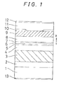
- Fig. 1 is a view showing an embodiment of the invention.
- AlGaAs type materials have a tendency of the band gap to widen with increase in Al composition.
- the band gaps of the optical guide layers 4, 8 are wider than that of the active layer 6, the band gaps of the cladding layers 3, 9 are wider than those of the optical guide layers 4, 8, and the band gaps of the carrier blocking layers 5, 7 are wider than those of the optical guide layers 4, 8.
- the electric current is injected into the active layer 6 as a carrier, and then the carrier re-combines to emit light. Further, as the injection amount of current increases, induced emission starts, and finally laser oscillation starts to occur between facets which construct an optical resonator, in the vertical direction on the sheet of Fig. 1.
- the laser light is distributed through the optical guide layers 4, 8 and the cladding layers 3, 9 disposed on both faces of the active layer 6, and is then guided.
- the carrier in the active layer 6 is confined in the active layer due to the existence of the carrier blocking layers 5, 7, so that an improvement in recombination efficiency is attained.
- a semiconductor laser device of the reference example is formed in accordance with the embodiment of Fig. 1, while the refractive index and thickness of the n-type cladding layer 3 are identical to those of the p-type cladding layer 9, wherein the refractive index is 3.354 and the thickness t is 1.1 ⁇ m.
- Fig. 2 is a graph showing wave guide modes of the embodiment and the reference example.
- the horizontal axis indicates positions in the direction of layer-thickness with respect to the active layer 6 (unit: ⁇ m), and the vertical axis indicates intensities of light (arbitrary unit, linear).
- the p-type cladding layer is formed so as to have a refractive index lower than that of the n-type cladding layer, whereby a wave guide mode of the embodiment is pushed out to the side of the n-type layer (negative side) as a whole, as compared with the reference example (shown by a dotted line).
- This configuration decreases the distribution amounts of wave guide mode at the p-type guide layer and at the p-type cladding layer, thereby making it possible to decrease inner losses due to free carrier absorption.
- the embodiment herein shows a case where both the refractive index and the thickness of the n-type cladding layer 3 are different from those of the p-type cladding layer 9.
- a wave guide mode will be shown by the same solid line of Fig. 2, and free carrier absorption at the p-type guide layer and the p-type cladding layer can be reduced in the same fashion.
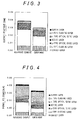
- Fig. 3 is a graph showing the electric resistances of the embodiment and the reference example, wherein the vertical axis indicates the electric resistance ( ⁇ ) and the order of layers as shown in Fig. 1 is turned upside down. It is apparent from this graph that among the respective layers constructing a semiconductor laser, the p-type cladding layer has the highest electric resistance. Moreover, it is apparent that in the embodiment, the p-type cladding layer is made so as to have a smaller thickness than that of the n-type cladding layer, whereby the electric resistance of the p-type cladding layer can be decreased to about 60 % as compared with the reference example, and the whole electric resistance can be also reduced to a large extent.
- Fig. 4 is a graph showing the thermal resistances of the embodiment and the reference example, wherein the vertical axis indicates the thermal resistance (K / W) and the order of layers as shown in Fig. 1 is turned upside down. It is apparent from this graph that among the respective layers constructing a semiconductor laser, the p-type cladding layer and the n-type cladding layer have considerably high thermal resistances. Moreover, it is apparent that in the embodiment, the p-type cladding layer is made so as to have a smaller thickness than that of the n-type cladding layer, whereby the thermal resistance of the p-type cladding layer can be decreased to about 40 % as compared with the reference example, and the whole thermal resistance can be also reduced to a large extent. In particular, in a case where a semiconductor laser is mounted by junction down, the embodiment will be advantageous because the thermal resistance on the side of the p-type layer of the active layer is decreased.
Landscapes
- Physics & Mathematics (AREA)
- Optics & Photonics (AREA)
- Electromagnetism (AREA)
- Engineering & Computer Science (AREA)
- General Physics & Mathematics (AREA)
- Condensed Matter Physics & Semiconductors (AREA)
- Chemical & Material Sciences (AREA)
- Geometry (AREA)
- Nanotechnology (AREA)
- Life Sciences & Earth Sciences (AREA)
- Biophysics (AREA)
- Crystallography & Structural Chemistry (AREA)
- Plasma & Fusion (AREA)
- Semiconductor Lasers (AREA)
Applications Claiming Priority (3)
| Application Number | Priority Date | Filing Date | Title |
|---|---|---|---|
| JP32476897 | 1997-11-26 | ||
| JP9324768A JPH11163458A (ja) | 1997-11-26 | 1997-11-26 | 半導体レーザ装置 |
| JP324768/97 | 1997-11-26 |
Publications (3)
| Publication Number | Publication Date |
|---|---|
| EP0920097A2 true EP0920097A2 (fr) | 1999-06-02 |
| EP0920097A3 EP0920097A3 (fr) | 2002-01-23 |
| EP0920097B1 EP0920097B1 (fr) | 2005-02-09 |
Family
ID=18169466
Family Applications (1)
| Application Number | Title | Priority Date | Filing Date |
|---|---|---|---|
| EP98309626A Expired - Lifetime EP0920097B1 (fr) | 1997-11-26 | 1998-11-24 | Dispositif laser à semi-conducteur |
Country Status (8)
| Country | Link |
|---|---|
| US (1) | US6175582B1 (fr) |
| EP (1) | EP0920097B1 (fr) |
| JP (1) | JPH11163458A (fr) |
| KR (1) | KR19990045620A (fr) |
| CN (1) | CN1121084C (fr) |
| CA (1) | CA2254484A1 (fr) |
| DE (1) | DE69828942T2 (fr) |
| TW (1) | TW472420B (fr) |
Cited By (3)
| Publication number | Priority date | Publication date | Assignee | Title |
|---|---|---|---|---|
| EP1079485A1 (fr) * | 1999-08-27 | 2001-02-28 | Mitsui Chemicals, Inc. | Laser à semiconducteur |
| JP2003524890A (ja) * | 2000-01-20 | 2003-08-19 | プリンストン・ライトウェーブ・インコーポレイテッド | 改良されたビームダイバージェンス優先順位を有する半導体ダイオードレーザ |
| EP1416598A3 (fr) * | 2002-11-01 | 2005-06-08 | Anritsu Corporation | Appareil semiconducteur emmeteur de lumière permettant d'obtenir une haute puissance optique de sortie avec une structure simple |
Families Citing this family (64)
| Publication number | Priority date | Publication date | Assignee | Title |
|---|---|---|---|---|
| EP1087480B1 (fr) | 1999-09-27 | 2006-11-15 | Sanyo Electric Co., Ltd. | Dispositif laser à semiconducteur et méthode de fabrication |
| JP4105857B2 (ja) * | 2001-08-13 | 2008-06-25 | ローム株式会社 | 半導体レーザ素子 |
| US6819696B1 (en) * | 2001-09-21 | 2004-11-16 | The United States Of America As Represented By The Secretary Of The Army | Intersubband semiconductor lasers with enhanced subband depopulation rate |
| FR2833418B1 (fr) * | 2001-12-06 | 2004-04-09 | Cit Alcatel | Composant optique de type laser a semiconducteur |
| US7676390B2 (en) * | 2003-09-04 | 2010-03-09 | General Electric Company | Techniques for performing business analysis based on incomplete and/or stage-based data |
| JP2006270028A (ja) * | 2005-02-25 | 2006-10-05 | Mitsubishi Electric Corp | 半導体発光素子 |
| JP4842668B2 (ja) * | 2006-02-24 | 2011-12-21 | シャープ株式会社 | 半導体レーザ素子とその製造方法、および光無線通信用送信装置、光ディスク装置 |
| JP2010135724A (ja) | 2008-10-27 | 2010-06-17 | Mitsubishi Electric Corp | 半導体レーザ装置 |
| US8273617B2 (en) | 2009-09-30 | 2012-09-25 | Suvolta, Inc. | Electronic devices and systems, and methods for making and using the same |
| US20110079861A1 (en) * | 2009-09-30 | 2011-04-07 | Lucian Shifren | Advanced Transistors with Threshold Voltage Set Dopant Structures |
| US8421162B2 (en) | 2009-09-30 | 2013-04-16 | Suvolta, Inc. | Advanced transistors with punch through suppression |
| US8530286B2 (en) | 2010-04-12 | 2013-09-10 | Suvolta, Inc. | Low power semiconductor transistor structure and method of fabrication thereof |
| US8569128B2 (en) | 2010-06-21 | 2013-10-29 | Suvolta, Inc. | Semiconductor structure and method of fabrication thereof with mixed metal types |
| US8377783B2 (en) | 2010-09-30 | 2013-02-19 | Suvolta, Inc. | Method for reducing punch-through in a transistor device |
| US8404551B2 (en) | 2010-12-03 | 2013-03-26 | Suvolta, Inc. | Source/drain extension control for advanced transistors |
| US8461875B1 (en) | 2011-02-18 | 2013-06-11 | Suvolta, Inc. | Digital circuits having improved transistors, and methods therefor |
| US8525271B2 (en) | 2011-03-03 | 2013-09-03 | Suvolta, Inc. | Semiconductor structure with improved channel stack and method for fabrication thereof |
| US8400219B2 (en) | 2011-03-24 | 2013-03-19 | Suvolta, Inc. | Analog circuits having improved transistors, and methods therefor |
| US8748270B1 (en) | 2011-03-30 | 2014-06-10 | Suvolta, Inc. | Process for manufacturing an improved analog transistor |
| US8796048B1 (en) | 2011-05-11 | 2014-08-05 | Suvolta, Inc. | Monitoring and measurement of thin film layers |
| US8999861B1 (en) | 2011-05-11 | 2015-04-07 | Suvolta, Inc. | Semiconductor structure with substitutional boron and method for fabrication thereof |
| US8811068B1 (en) | 2011-05-13 | 2014-08-19 | Suvolta, Inc. | Integrated circuit devices and methods |
| US8569156B1 (en) | 2011-05-16 | 2013-10-29 | Suvolta, Inc. | Reducing or eliminating pre-amorphization in transistor manufacture |
| US8735987B1 (en) | 2011-06-06 | 2014-05-27 | Suvolta, Inc. | CMOS gate stack structures and processes |
| US8995204B2 (en) | 2011-06-23 | 2015-03-31 | Suvolta, Inc. | Circuit devices and methods having adjustable transistor body bias |
| US8629016B1 (en) | 2011-07-26 | 2014-01-14 | Suvolta, Inc. | Multiple transistor types formed in a common epitaxial layer by differential out-diffusion from a doped underlayer |
| US8748986B1 (en) | 2011-08-05 | 2014-06-10 | Suvolta, Inc. | Electronic device with controlled threshold voltage |
| KR101891373B1 (ko) | 2011-08-05 | 2018-08-24 | 엠아이이 후지쯔 세미컨덕터 리미티드 | 핀 구조물을 갖는 반도체 디바이스 및 그 제조 방법 |
| US8645878B1 (en) | 2011-08-23 | 2014-02-04 | Suvolta, Inc. | Porting a circuit design from a first semiconductor process to a second semiconductor process |
| US8614128B1 (en) | 2011-08-23 | 2013-12-24 | Suvolta, Inc. | CMOS structures and processes based on selective thinning |
| US8713511B1 (en) | 2011-09-16 | 2014-04-29 | Suvolta, Inc. | Tools and methods for yield-aware semiconductor manufacturing process target generation |
| US9236466B1 (en) | 2011-10-07 | 2016-01-12 | Mie Fujitsu Semiconductor Limited | Analog circuits having improved insulated gate transistors, and methods therefor |
| US8895327B1 (en) | 2011-12-09 | 2014-11-25 | Suvolta, Inc. | Tipless transistors, short-tip transistors, and methods and circuits therefor |
| US8819603B1 (en) | 2011-12-15 | 2014-08-26 | Suvolta, Inc. | Memory circuits and methods of making and designing the same |
| US8883600B1 (en) | 2011-12-22 | 2014-11-11 | Suvolta, Inc. | Transistor having reduced junction leakage and methods of forming thereof |
| US8599623B1 (en) | 2011-12-23 | 2013-12-03 | Suvolta, Inc. | Circuits and methods for measuring circuit elements in an integrated circuit device |
| US8970289B1 (en) | 2012-01-23 | 2015-03-03 | Suvolta, Inc. | Circuits and devices for generating bi-directional body bias voltages, and methods therefor |
| US8877619B1 (en) | 2012-01-23 | 2014-11-04 | Suvolta, Inc. | Process for manufacture of integrated circuits with different channel doping transistor architectures and devices therefrom |
| US9093550B1 (en) | 2012-01-31 | 2015-07-28 | Mie Fujitsu Semiconductor Limited | Integrated circuits having a plurality of high-K metal gate FETs with various combinations of channel foundation structure and gate stack structure and methods of making same |
| US9406567B1 (en) | 2012-02-28 | 2016-08-02 | Mie Fujitsu Semiconductor Limited | Method for fabricating multiple transistor devices on a substrate with varying threshold voltages |
| US8863064B1 (en) | 2012-03-23 | 2014-10-14 | Suvolta, Inc. | SRAM cell layout structure and devices therefrom |
| US9299698B2 (en) | 2012-06-27 | 2016-03-29 | Mie Fujitsu Semiconductor Limited | Semiconductor structure with multiple transistors having various threshold voltages |
| US8637955B1 (en) | 2012-08-31 | 2014-01-28 | Suvolta, Inc. | Semiconductor structure with reduced junction leakage and method of fabrication thereof |
| US9112057B1 (en) | 2012-09-18 | 2015-08-18 | Mie Fujitsu Semiconductor Limited | Semiconductor devices with dopant migration suppression and method of fabrication thereof |
| US9041126B2 (en) | 2012-09-21 | 2015-05-26 | Mie Fujitsu Semiconductor Limited | Deeply depleted MOS transistors having a screening layer and methods thereof |
| WO2014071049A2 (fr) | 2012-10-31 | 2014-05-08 | Suvolta, Inc. | Dispositif du type dram à circuits périphériques à transistors à faible variations, et procédés associés |
| US8816754B1 (en) | 2012-11-02 | 2014-08-26 | Suvolta, Inc. | Body bias circuits and methods |
| US9093997B1 (en) | 2012-11-15 | 2015-07-28 | Mie Fujitsu Semiconductor Limited | Slew based process and bias monitors and related methods |
| US9070477B1 (en) | 2012-12-12 | 2015-06-30 | Mie Fujitsu Semiconductor Limited | Bit interleaved low voltage static random access memory (SRAM) and related methods |
| US9112484B1 (en) | 2012-12-20 | 2015-08-18 | Mie Fujitsu Semiconductor Limited | Integrated circuit process and bias monitors and related methods |
| US9268885B1 (en) | 2013-02-28 | 2016-02-23 | Mie Fujitsu Semiconductor Limited | Integrated circuit device methods and models with predicted device metric variations |
| US8994415B1 (en) | 2013-03-01 | 2015-03-31 | Suvolta, Inc. | Multiple VDD clock buffer |
| US8988153B1 (en) | 2013-03-09 | 2015-03-24 | Suvolta, Inc. | Ring oscillator with NMOS or PMOS variation insensitivity |
| US9299801B1 (en) | 2013-03-14 | 2016-03-29 | Mie Fujitsu Semiconductor Limited | Method for fabricating a transistor device with a tuned dopant profile |
| US9112495B1 (en) | 2013-03-15 | 2015-08-18 | Mie Fujitsu Semiconductor Limited | Integrated circuit device body bias circuits and methods |
| US9449967B1 (en) | 2013-03-15 | 2016-09-20 | Fujitsu Semiconductor Limited | Transistor array structure |
| JP2014212186A (ja) * | 2013-04-18 | 2014-11-13 | シャープ株式会社 | 半導体レーザ素子 |
| US9478571B1 (en) | 2013-05-24 | 2016-10-25 | Mie Fujitsu Semiconductor Limited | Buried channel deeply depleted channel transistor |
| US8976575B1 (en) | 2013-08-29 | 2015-03-10 | Suvolta, Inc. | SRAM performance monitor |
| US9710006B2 (en) | 2014-07-25 | 2017-07-18 | Mie Fujitsu Semiconductor Limited | Power up body bias circuits and methods |
| US9319013B2 (en) | 2014-08-19 | 2016-04-19 | Mie Fujitsu Semiconductor Limited | Operational amplifier input offset correction with transistor threshold voltage adjustment |
| CN109417274B (zh) * | 2016-06-30 | 2021-12-07 | 新唐科技日本株式会社 | 半导体激光装置、半导体激光模块及熔接用激光光源系统 |
| WO2018003551A1 (fr) * | 2016-06-30 | 2018-01-04 | パナソニックIpマネジメント株式会社 | Dispositif laser à semiconducteur, module laser à semiconducteur et système de source de lumière laser pour soudage |
| KR102661948B1 (ko) * | 2018-01-19 | 2024-04-29 | 삼성전자주식회사 | 반도체 레이저 장치 및 그 제조 방법 |
Family Cites Families (16)
| Publication number | Priority date | Publication date | Assignee | Title |
|---|---|---|---|---|
| US3855607A (en) * | 1973-05-29 | 1974-12-17 | Rca Corp | Semiconductor injection laser with reduced divergence of emitted beam |
| CA1137605A (fr) * | 1979-01-15 | 1982-12-14 | Donald R. Scifres | Laser a grande puissance |
| DE68909632T2 (de) * | 1988-02-09 | 1994-03-10 | Toshiba Kawasaki Kk | Halbleiterlaser-Vorrichtung und deren Herstellungsverfahren. |
| JP2821150B2 (ja) | 1988-10-21 | 1998-11-05 | シャープ株式会社 | 半導体レーザ素子 |
| JPH04144185A (ja) * | 1990-10-04 | 1992-05-18 | Mitsubishi Electric Corp | 半導体レーザ装置 |
| CA2106562C (fr) | 1992-02-05 | 1999-05-04 | Mitsui Chemicals, Inc. | Element de laser a semiconducteur et laser utilisant cet element |
| US5301202A (en) * | 1993-02-25 | 1994-04-05 | International Business Machines, Corporation | Semiconductor ridge waveguide laser with asymmetrical cladding |
| JPH07231139A (ja) | 1993-12-24 | 1995-08-29 | Mitsui Petrochem Ind Ltd | 半導体レーザ素子 |
| CA2138912C (fr) * | 1993-12-24 | 1999-05-04 | Shoji Ishizaka | Laser a semiconducteur |
| JPH0883613A (ja) * | 1994-09-12 | 1996-03-26 | Furukawa Battery Co Ltd:The | 水素吸蔵合金電極用スラリーの製造方法 |
| DE69517044T2 (de) * | 1994-10-18 | 2000-10-26 | Mitsui Chemicals, Inc. | Halbleiterlaservorrichtung |
| US5617437A (en) * | 1994-11-24 | 1997-04-01 | Fuji Photo Film Co., Ltd. | Semiconductor laser |
| US5539762A (en) * | 1995-05-12 | 1996-07-23 | At&T Corp. | Article comprising a semiconductor laser with carrier stopper layer |
| JPH0936479A (ja) * | 1995-07-21 | 1997-02-07 | Matsushita Electric Ind Co Ltd | 半導体レーザおよびその製造方法 |
| EP0772249B1 (fr) * | 1995-11-06 | 2006-05-03 | Nichia Corporation | Dispositif semi-conducteur comprenant un composé de nitrure |
| US5727012A (en) * | 1996-03-07 | 1998-03-10 | Lucent Technologies Inc. | Heterostructure laser |
-
1997
- 1997-11-26 JP JP9324768A patent/JPH11163458A/ja active Pending
-
1998
- 1998-11-23 TW TW087119375A patent/TW472420B/zh not_active IP Right Cessation
- 1998-11-24 DE DE69828942T patent/DE69828942T2/de not_active Expired - Lifetime
- 1998-11-24 CA CA002254484A patent/CA2254484A1/fr not_active Abandoned
- 1998-11-24 EP EP98309626A patent/EP0920097B1/fr not_active Expired - Lifetime
- 1998-11-25 US US09/199,435 patent/US6175582B1/en not_active Expired - Lifetime
- 1998-11-26 KR KR1019980051075A patent/KR19990045620A/ko not_active Ceased
- 1998-11-26 CN CN98122371A patent/CN1121084C/zh not_active Expired - Fee Related
Cited By (6)
| Publication number | Priority date | Publication date | Assignee | Title |
|---|---|---|---|---|
| EP1079485A1 (fr) * | 1999-08-27 | 2001-02-28 | Mitsui Chemicals, Inc. | Laser à semiconducteur |
| US6546032B1 (en) | 1999-08-27 | 2003-04-08 | Mitsui Chemicals, Inc. | Semiconductor laser apparatus |
| JP2003524890A (ja) * | 2000-01-20 | 2003-08-19 | プリンストン・ライトウェーブ・インコーポレイテッド | 改良されたビームダイバージェンス優先順位を有する半導体ダイオードレーザ |
| EP1258062A4 (fr) * | 2000-01-20 | 2006-01-11 | Trumpf Photonics Inc | Lasers a diode a semi-conducteurs dotes d'une priorite de divergence amelioree |
| EP1416598A3 (fr) * | 2002-11-01 | 2005-06-08 | Anritsu Corporation | Appareil semiconducteur emmeteur de lumière permettant d'obtenir une haute puissance optique de sortie avec une structure simple |
| US6987285B2 (en) | 2002-11-01 | 2006-01-17 | Anritsu Corporation | Semiconductor light emitting device in which high-power light output can be obtained with a simple structure including InGaAsP active layer not less than 3.5 microns and InGaAsP and InP cladding |
Also Published As
| Publication number | Publication date |
|---|---|
| KR19990045620A (ko) | 1999-06-25 |
| DE69828942D1 (de) | 2005-03-17 |
| JPH11163458A (ja) | 1999-06-18 |
| CN1121084C (zh) | 2003-09-10 |
| CN1218319A (zh) | 1999-06-02 |
| EP0920097A3 (fr) | 2002-01-23 |
| DE69828942T2 (de) | 2006-04-13 |
| EP0920097B1 (fr) | 2005-02-09 |
| TW472420B (en) | 2002-01-11 |
| US6175582B1 (en) | 2001-01-16 |
| CA2254484A1 (fr) | 1999-05-26 |
Similar Documents
| Publication | Publication Date | Title |
|---|---|---|
| US6175582B1 (en) | Semiconductor laser device | |
| US6563850B1 (en) | Light-emitting device and fabricating method thereof | |
| US6584130B2 (en) | Multiple semiconductor laser structure with narrow wavelength distribution | |
| EP0805533B1 (fr) | Element de laser a semi-conducteur | |
| JP4497859B2 (ja) | 面発光半導体レーザ装置および光伝送モジュールおよび光伝送システム | |
| US20020041613A1 (en) | Semiconductor laser device and opticlal fiber amplifier using the same | |
| CN114465090A (zh) | 一种多结分布式反馈激光器及其制备方法 | |
| US6961358B2 (en) | Semiconductor laser | |
| WO2023281902A1 (fr) | Élément émetteur de lumière à semi-conducteur au nitrure | |
| US4759025A (en) | Window structure semiconductor laser | |
| JP3869106B2 (ja) | 面発光レーザ装置 | |
| US6493132B1 (en) | Monolithic optically pumped high power semiconductor lasers and amplifiers | |
| JP2927661B2 (ja) | スーパールミネッセントダイオード素子およびその製造方法 | |
| JPH0945986A (ja) | 半導体レーザ素子 | |
| US4989213A (en) | Narrow divergence, single quantum well, separate confinement, algaas laser | |
| JPH11163459A (ja) | 半導体レーザ装置 | |
| JP2007087994A (ja) | 面発光半導体レーザ素子 | |
| JP2004095822A (ja) | 半導体レーザ素子 | |
| JPH11220208A (ja) | 半導体レーザダイオード | |
| JPH07335969A (ja) | 半導体レーザ素子及び半導体レーザアレイ素子 | |
| WO2023247129A1 (fr) | Diode laser à semi-conducteur à émission par la surface | |
| JP3408247B2 (ja) | 半導体レーザ素子 | |
| KR100224877B1 (ko) | 표면광 레이저 | |
| US20020146048A1 (en) | Semiconductor laser device | |
| JP2855887B2 (ja) | 半導体レーザ及びその製造方法 |
Legal Events
| Date | Code | Title | Description |
|---|---|---|---|
| PUAI | Public reference made under article 153(3) epc to a published international application that has entered the european phase |
Free format text: ORIGINAL CODE: 0009012 |
|
| AK | Designated contracting states |
Kind code of ref document: A2 Designated state(s): AT BE CH CY DE DK ES FI FR GB GR IE IT LI LU MC NL PT SE Kind code of ref document: A2 Designated state(s): CH DE FR GB IT LI NL |
|
| AX | Request for extension of the european patent |
Free format text: AL;LT;LV;MK;RO;SI |
|
| PUAL | Search report despatched |
Free format text: ORIGINAL CODE: 0009013 |
|
| AK | Designated contracting states |
Kind code of ref document: A3 Designated state(s): AT BE CH CY DE DK ES FI FR GB GR IE IT LI LU MC NL PT SE |
|
| AX | Request for extension of the european patent |
Free format text: AL;LT;LV;MK;RO;SI |
|
| 17P | Request for examination filed |
Effective date: 20020321 |
|
| AKX | Designation fees paid |
Free format text: CH DE FR GB IT LI NL |
|
| 17Q | First examination report despatched |
Effective date: 20040205 |
|
| GRAP | Despatch of communication of intention to grant a patent |
Free format text: ORIGINAL CODE: EPIDOSNIGR1 |
|
| RAP1 | Party data changed (applicant data changed or rights of an application transferred) |
Owner name: MITSUI CHEMICALS, INC. |
|
| GRAS | Grant fee paid |
Free format text: ORIGINAL CODE: EPIDOSNIGR3 |
|
| GRAA | (expected) grant |
Free format text: ORIGINAL CODE: 0009210 |
|
| AK | Designated contracting states |
Kind code of ref document: B1 Designated state(s): CH DE FR GB IT LI NL |
|
| PG25 | Lapsed in a contracting state [announced via postgrant information from national office to epo] |
Ref country code: NL Free format text: LAPSE BECAUSE OF FAILURE TO SUBMIT A TRANSLATION OF THE DESCRIPTION OR TO PAY THE FEE WITHIN THE PRESCRIBED TIME-LIMIT Effective date: 20050209 Ref country code: LI Free format text: LAPSE BECAUSE OF FAILURE TO SUBMIT A TRANSLATION OF THE DESCRIPTION OR TO PAY THE FEE WITHIN THE PRESCRIBED TIME-LIMIT Effective date: 20050209 Ref country code: IT Free format text: LAPSE BECAUSE OF FAILURE TO SUBMIT A TRANSLATION OF THE DESCRIPTION OR TO PAY THE FEE WITHIN THE PRE;WARNING: LAPSES OF ITALIAN PATENTS WITH EFFECTIVE DATE BEFORE 2007 MAY HAVE OCCURRED AT ANY TIME BEFORE 2007. THE CORRECT EFFECTIVE DATE MAY BE DIFFERENT FROM THE ONE RECORDED.SCRIBED TIME-LIMIT Effective date: 20050209 Ref country code: CH Free format text: LAPSE BECAUSE OF FAILURE TO SUBMIT A TRANSLATION OF THE DESCRIPTION OR TO PAY THE FEE WITHIN THE PRESCRIBED TIME-LIMIT Effective date: 20050209 |
|
| REG | Reference to a national code |
Ref country code: GB Ref legal event code: FG4D |
|
| RIC1 | Information provided on ipc code assigned before grant |
Ipc: 7H 01S 5/20 A |
|
| REG | Reference to a national code |
Ref country code: CH Ref legal event code: EP |
|
| REG | Reference to a national code |
Ref country code: IE Ref legal event code: FG4D |
|
| REF | Corresponds to: |
Ref document number: 69828942 Country of ref document: DE Date of ref document: 20050317 Kind code of ref document: P |
|
| NLV1 | Nl: lapsed or annulled due to failure to fulfill the requirements of art. 29p and 29m of the patents act | ||
| REG | Reference to a national code |
Ref country code: CH Ref legal event code: PL |
|
| PLBE | No opposition filed within time limit |
Free format text: ORIGINAL CODE: 0009261 |
|
| STAA | Information on the status of an ep patent application or granted ep patent |
Free format text: STATUS: NO OPPOSITION FILED WITHIN TIME LIMIT |
|
| ET | Fr: translation filed | ||
| 26N | No opposition filed |
Effective date: 20051110 |
|
| PGFP | Annual fee paid to national office [announced via postgrant information from national office to epo] |
Ref country code: FR Payment date: 20121130 Year of fee payment: 15 |
|
| PGFP | Annual fee paid to national office [announced via postgrant information from national office to epo] |
Ref country code: GB Payment date: 20121121 Year of fee payment: 15 |
|
| PGFP | Annual fee paid to national office [announced via postgrant information from national office to epo] |
Ref country code: DE Payment date: 20131120 Year of fee payment: 16 |
|
| GBPC | Gb: european patent ceased through non-payment of renewal fee |
Effective date: 20131124 |
|
| REG | Reference to a national code |
Ref country code: FR Ref legal event code: ST Effective date: 20140731 |
|
| PG25 | Lapsed in a contracting state [announced via postgrant information from national office to epo] |
Ref country code: FR Free format text: LAPSE BECAUSE OF NON-PAYMENT OF DUE FEES Effective date: 20131202 Ref country code: GB Free format text: LAPSE BECAUSE OF NON-PAYMENT OF DUE FEES Effective date: 20131124 |
|
| REG | Reference to a national code |
Ref country code: DE Ref legal event code: R119 Ref document number: 69828942 Country of ref document: DE |
|
| PG25 | Lapsed in a contracting state [announced via postgrant information from national office to epo] |
Ref country code: DE Free format text: LAPSE BECAUSE OF NON-PAYMENT OF DUE FEES Effective date: 20150602 |