EP1087480B1 - Dispositif laser à semiconducteur et méthode de fabrication - Google Patents
Dispositif laser à semiconducteur et méthode de fabrication Download PDFInfo
- Publication number
- EP1087480B1 EP1087480B1 EP00308345A EP00308345A EP1087480B1 EP 1087480 B1 EP1087480 B1 EP 1087480B1 EP 00308345 A EP00308345 A EP 00308345A EP 00308345 A EP00308345 A EP 00308345A EP 1087480 B1 EP1087480 B1 EP 1087480B1
- Authority
- EP
- European Patent Office
- Prior art keywords
- layer
- semiconductor laser
- laser device
- type
- ridge portion
- Prior art date
- Legal status (The legal status is an assumption and is not a legal conclusion. Google has not performed a legal analysis and makes no representation as to the accuracy of the status listed.)
- Expired - Lifetime
Links
- 239000004065 semiconductor Substances 0.000 title claims description 79
- 238000004519 manufacturing process Methods 0.000 title claims description 19
- 230000000903 blocking effect Effects 0.000 claims description 71
- 238000005253 cladding Methods 0.000 claims description 67
- 239000000203 mixture Substances 0.000 claims description 51
- 239000000758 substrate Substances 0.000 claims description 39
- 238000005530 etching Methods 0.000 claims description 21
- 229910052782 aluminium Inorganic materials 0.000 claims description 17
- 229910052733 gallium Inorganic materials 0.000 claims description 17
- 238000000034 method Methods 0.000 claims description 3
- 229910000980 Aluminium gallium arsenide Inorganic materials 0.000 description 33
- 229910001218 Gallium arsenide Inorganic materials 0.000 description 18
- 239000007789 gas Substances 0.000 description 17
- 239000000463 material Substances 0.000 description 16
- RBFQJDQYXXHULB-UHFFFAOYSA-N arsane Chemical compound [AsH3] RBFQJDQYXXHULB-UHFFFAOYSA-N 0.000 description 11
- 229910000070 arsenic hydride Inorganic materials 0.000 description 10
- 230000009467 reduction Effects 0.000 description 8
- 239000002019 doping agent Substances 0.000 description 7
- 230000003287 optical effect Effects 0.000 description 6
- SPVXKVOXSXTJOY-UHFFFAOYSA-N selane Chemical compound [SeH2] SPVXKVOXSXTJOY-UHFFFAOYSA-N 0.000 description 6
- 229910000058 selane Inorganic materials 0.000 description 6
- HQWPLXHWEZZGKY-UHFFFAOYSA-N diethylzinc Chemical compound CC[Zn]CC HQWPLXHWEZZGKY-UHFFFAOYSA-N 0.000 description 5
- 238000001312 dry etching Methods 0.000 description 4
- 230000000694 effects Effects 0.000 description 4
- 238000001039 wet etching Methods 0.000 description 4
- MHAJPDPJQMAIIY-UHFFFAOYSA-N Hydrogen peroxide Chemical compound OO MHAJPDPJQMAIIY-UHFFFAOYSA-N 0.000 description 2
- BLRPTPMANUNPDV-UHFFFAOYSA-N Silane Chemical compound [SiH4] BLRPTPMANUNPDV-UHFFFAOYSA-N 0.000 description 2
- VYPSYNLAJGMNEJ-UHFFFAOYSA-N Silicium dioxide Chemical compound O=[Si]=O VYPSYNLAJGMNEJ-UHFFFAOYSA-N 0.000 description 2
- 230000004888 barrier function Effects 0.000 description 2
- 230000008859 change Effects 0.000 description 2
- 238000001451 molecular beam epitaxy Methods 0.000 description 2
- 238000001878 scanning electron micrograph Methods 0.000 description 2
- 238000002441 X-ray diffraction Methods 0.000 description 1
- 238000010521 absorption reaction Methods 0.000 description 1
- 238000005229 chemical vapour deposition Methods 0.000 description 1
- 229910052681 coesite Inorganic materials 0.000 description 1
- 229910052906 cristobalite Inorganic materials 0.000 description 1
- 230000006866 deterioration Effects 0.000 description 1
- 230000001747 exhibiting effect Effects 0.000 description 1
- 229910021478 group 5 element Inorganic materials 0.000 description 1
- 238000002347 injection Methods 0.000 description 1
- 239000007924 injection Substances 0.000 description 1
- 238000010884 ion-beam technique Methods 0.000 description 1
- 150000002500 ions Chemical class 0.000 description 1
- 238000000206 photolithography Methods 0.000 description 1
- 238000001020 plasma etching Methods 0.000 description 1
- 238000002360 preparation method Methods 0.000 description 1
- 239000002994 raw material Substances 0.000 description 1
- 239000000377 silicon dioxide Substances 0.000 description 1
- 229910052682 stishovite Inorganic materials 0.000 description 1
- 238000003860 storage Methods 0.000 description 1
- 230000007704 transition Effects 0.000 description 1
- 229910052905 tridymite Inorganic materials 0.000 description 1
- JLTRXTDYQLMHGR-UHFFFAOYSA-N trimethylaluminium Chemical compound C[Al](C)C JLTRXTDYQLMHGR-UHFFFAOYSA-N 0.000 description 1
- XCZXGTMEAKBVPV-UHFFFAOYSA-N trimethylgallium Chemical compound C[Ga](C)C XCZXGTMEAKBVPV-UHFFFAOYSA-N 0.000 description 1
- XLYOFNOQVPJJNP-UHFFFAOYSA-N water Substances O XLYOFNOQVPJJNP-UHFFFAOYSA-N 0.000 description 1
Images








Classifications
-
- H—ELECTRICITY
- H01—ELECTRIC ELEMENTS
- H01S—DEVICES USING THE PROCESS OF LIGHT AMPLIFICATION BY STIMULATED EMISSION OF RADIATION [LASER] TO AMPLIFY OR GENERATE LIGHT; DEVICES USING STIMULATED EMISSION OF ELECTROMAGNETIC RADIATION IN WAVE RANGES OTHER THAN OPTICAL
- H01S5/00—Semiconductor lasers
- H01S5/20—Structure or shape of the semiconductor body to guide the optical wave ; Confining structures perpendicular to the optical axis, e.g. index or gain guiding, stripe geometry, broad area lasers, gain tailoring, transverse or lateral reflectors, special cladding structures, MQW barrier reflection layers
-
- H—ELECTRICITY
- H01—ELECTRIC ELEMENTS
- H01S—DEVICES USING THE PROCESS OF LIGHT AMPLIFICATION BY STIMULATED EMISSION OF RADIATION [LASER] TO AMPLIFY OR GENERATE LIGHT; DEVICES USING STIMULATED EMISSION OF ELECTROMAGNETIC RADIATION IN WAVE RANGES OTHER THAN OPTICAL
- H01S5/00—Semiconductor lasers
- H01S5/20—Structure or shape of the semiconductor body to guide the optical wave ; Confining structures perpendicular to the optical axis, e.g. index or gain guiding, stripe geometry, broad area lasers, gain tailoring, transverse or lateral reflectors, special cladding structures, MQW barrier reflection layers
- H01S5/22—Structure or shape of the semiconductor body to guide the optical wave ; Confining structures perpendicular to the optical axis, e.g. index or gain guiding, stripe geometry, broad area lasers, gain tailoring, transverse or lateral reflectors, special cladding structures, MQW barrier reflection layers having a ridge or stripe structure
- H01S5/223—Buried stripe structure
- H01S5/2231—Buried stripe structure with inner confining structure only between the active layer and the upper electrode
-
- H—ELECTRICITY
- H01—ELECTRIC ELEMENTS
- H01S—DEVICES USING THE PROCESS OF LIGHT AMPLIFICATION BY STIMULATED EMISSION OF RADIATION [LASER] TO AMPLIFY OR GENERATE LIGHT; DEVICES USING STIMULATED EMISSION OF ELECTROMAGNETIC RADIATION IN WAVE RANGES OTHER THAN OPTICAL
- H01S2301/00—Functional characteristics
- H01S2301/18—Semiconductor lasers with special structural design for influencing the near- or far-field
-
- H—ELECTRICITY
- H01—ELECTRIC ELEMENTS
- H01S—DEVICES USING THE PROCESS OF LIGHT AMPLIFICATION BY STIMULATED EMISSION OF RADIATION [LASER] TO AMPLIFY OR GENERATE LIGHT; DEVICES USING STIMULATED EMISSION OF ELECTROMAGNETIC RADIATION IN WAVE RANGES OTHER THAN OPTICAL
- H01S5/00—Semiconductor lasers
- H01S5/20—Structure or shape of the semiconductor body to guide the optical wave ; Confining structures perpendicular to the optical axis, e.g. index or gain guiding, stripe geometry, broad area lasers, gain tailoring, transverse or lateral reflectors, special cladding structures, MQW barrier reflection layers
- H01S5/22—Structure or shape of the semiconductor body to guide the optical wave ; Confining structures perpendicular to the optical axis, e.g. index or gain guiding, stripe geometry, broad area lasers, gain tailoring, transverse or lateral reflectors, special cladding structures, MQW barrier reflection layers having a ridge or stripe structure
- H01S5/2205—Structure or shape of the semiconductor body to guide the optical wave ; Confining structures perpendicular to the optical axis, e.g. index or gain guiding, stripe geometry, broad area lasers, gain tailoring, transverse or lateral reflectors, special cladding structures, MQW barrier reflection layers having a ridge or stripe structure comprising special burying or current confinement layers
-
- H—ELECTRICITY
- H01—ELECTRIC ELEMENTS
- H01S—DEVICES USING THE PROCESS OF LIGHT AMPLIFICATION BY STIMULATED EMISSION OF RADIATION [LASER] TO AMPLIFY OR GENERATE LIGHT; DEVICES USING STIMULATED EMISSION OF ELECTROMAGNETIC RADIATION IN WAVE RANGES OTHER THAN OPTICAL
- H01S5/00—Semiconductor lasers
- H01S5/20—Structure or shape of the semiconductor body to guide the optical wave ; Confining structures perpendicular to the optical axis, e.g. index or gain guiding, stripe geometry, broad area lasers, gain tailoring, transverse or lateral reflectors, special cladding structures, MQW barrier reflection layers
- H01S5/22—Structure or shape of the semiconductor body to guide the optical wave ; Confining structures perpendicular to the optical axis, e.g. index or gain guiding, stripe geometry, broad area lasers, gain tailoring, transverse or lateral reflectors, special cladding structures, MQW barrier reflection layers having a ridge or stripe structure
- H01S5/2205—Structure or shape of the semiconductor body to guide the optical wave ; Confining structures perpendicular to the optical axis, e.g. index or gain guiding, stripe geometry, broad area lasers, gain tailoring, transverse or lateral reflectors, special cladding structures, MQW barrier reflection layers having a ridge or stripe structure comprising special burying or current confinement layers
- H01S5/2206—Structure or shape of the semiconductor body to guide the optical wave ; Confining structures perpendicular to the optical axis, e.g. index or gain guiding, stripe geometry, broad area lasers, gain tailoring, transverse or lateral reflectors, special cladding structures, MQW barrier reflection layers having a ridge or stripe structure comprising special burying or current confinement layers based on III-V materials
- H01S5/221—Structure or shape of the semiconductor body to guide the optical wave ; Confining structures perpendicular to the optical axis, e.g. index or gain guiding, stripe geometry, broad area lasers, gain tailoring, transverse or lateral reflectors, special cladding structures, MQW barrier reflection layers having a ridge or stripe structure comprising special burying or current confinement layers based on III-V materials containing aluminium
-
- H—ELECTRICITY
- H01—ELECTRIC ELEMENTS
- H01S—DEVICES USING THE PROCESS OF LIGHT AMPLIFICATION BY STIMULATED EMISSION OF RADIATION [LASER] TO AMPLIFY OR GENERATE LIGHT; DEVICES USING STIMULATED EMISSION OF ELECTROMAGNETIC RADIATION IN WAVE RANGES OTHER THAN OPTICAL
- H01S5/00—Semiconductor lasers
- H01S5/20—Structure or shape of the semiconductor body to guide the optical wave ; Confining structures perpendicular to the optical axis, e.g. index or gain guiding, stripe geometry, broad area lasers, gain tailoring, transverse or lateral reflectors, special cladding structures, MQW barrier reflection layers
- H01S5/22—Structure or shape of the semiconductor body to guide the optical wave ; Confining structures perpendicular to the optical axis, e.g. index or gain guiding, stripe geometry, broad area lasers, gain tailoring, transverse or lateral reflectors, special cladding structures, MQW barrier reflection layers having a ridge or stripe structure
- H01S5/2205—Structure or shape of the semiconductor body to guide the optical wave ; Confining structures perpendicular to the optical axis, e.g. index or gain guiding, stripe geometry, broad area lasers, gain tailoring, transverse or lateral reflectors, special cladding structures, MQW barrier reflection layers having a ridge or stripe structure comprising special burying or current confinement layers
- H01S5/2218—Structure or shape of the semiconductor body to guide the optical wave ; Confining structures perpendicular to the optical axis, e.g. index or gain guiding, stripe geometry, broad area lasers, gain tailoring, transverse or lateral reflectors, special cladding structures, MQW barrier reflection layers having a ridge or stripe structure comprising special burying or current confinement layers having special optical properties
- H01S5/222—Structure or shape of the semiconductor body to guide the optical wave ; Confining structures perpendicular to the optical axis, e.g. index or gain guiding, stripe geometry, broad area lasers, gain tailoring, transverse or lateral reflectors, special cladding structures, MQW barrier reflection layers having a ridge or stripe structure comprising special burying or current confinement layers having special optical properties having a refractive index lower than that of the cladding layers or outer guiding layers
-
- H—ELECTRICITY
- H01—ELECTRIC ELEMENTS
- H01S—DEVICES USING THE PROCESS OF LIGHT AMPLIFICATION BY STIMULATED EMISSION OF RADIATION [LASER] TO AMPLIFY OR GENERATE LIGHT; DEVICES USING STIMULATED EMISSION OF ELECTROMAGNETIC RADIATION IN WAVE RANGES OTHER THAN OPTICAL
- H01S5/00—Semiconductor lasers
- H01S5/20—Structure or shape of the semiconductor body to guide the optical wave ; Confining structures perpendicular to the optical axis, e.g. index or gain guiding, stripe geometry, broad area lasers, gain tailoring, transverse or lateral reflectors, special cladding structures, MQW barrier reflection layers
- H01S5/22—Structure or shape of the semiconductor body to guide the optical wave ; Confining structures perpendicular to the optical axis, e.g. index or gain guiding, stripe geometry, broad area lasers, gain tailoring, transverse or lateral reflectors, special cladding structures, MQW barrier reflection layers having a ridge or stripe structure
- H01S5/2205—Structure or shape of the semiconductor body to guide the optical wave ; Confining structures perpendicular to the optical axis, e.g. index or gain guiding, stripe geometry, broad area lasers, gain tailoring, transverse or lateral reflectors, special cladding structures, MQW barrier reflection layers having a ridge or stripe structure comprising special burying or current confinement layers
- H01S5/2222—Structure or shape of the semiconductor body to guide the optical wave ; Confining structures perpendicular to the optical axis, e.g. index or gain guiding, stripe geometry, broad area lasers, gain tailoring, transverse or lateral reflectors, special cladding structures, MQW barrier reflection layers having a ridge or stripe structure comprising special burying or current confinement layers having special electric properties
- H01S5/2227—Structure or shape of the semiconductor body to guide the optical wave ; Confining structures perpendicular to the optical axis, e.g. index or gain guiding, stripe geometry, broad area lasers, gain tailoring, transverse or lateral reflectors, special cladding structures, MQW barrier reflection layers having a ridge or stripe structure comprising special burying or current confinement layers having special electric properties special thin layer sequence
Definitions
- the present invention relates to a semiconductor laser device preferably applied to an optical disk system or the like and a method of manufacturing the same.
- Optical disk systems employing disk-shaped optical recording media such as CD-ROMs or DVD-ROMs are indispensable as the storage media for personal computers. In such optical disk systems, transition from a reproduction only type to a writing type and to a rewritable type is getting obvious.
- a semiconductor laser device which is a key device for an optical disk system, is strongly required to have a high output in order to improve the writing speed of the optical disk system.
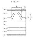
- Fig. 17 shows the basic structure of a typical conventional ridge type semiconductor laser device.
- a GaAs-based semiconductor laser device for example, an n-type buffer layer 702 of n-type GaAs, an n-type cladding layer 703 of n-type AlGaAs, an emission layer of AlGaAs and a p-type cladding layer 705 of p-type AlGaAs are formed on an n-type semiconductor substrate 701 of n-type GaAs.
- the p-type cladding layer 705 has a striped ridge portion provided with a central portion having a larger thickness than those of flat side portions for transverse mode control of the semiconductor laser device.
- An n-type blocking layer 706 of n-type AlGaAs is formed on the side surfaces and flat surfaces of the p-type cladding layer 705, in order to limit a current injection region.
- a p-type contact layer 707 of p-type GaAs is formed on the p-type cladding layer 705 and the n-type blocking layer 706.
- An n-type electrode 708 is formed on the rear surface of the n-type semiconductor substrate 701, while a p-type electrode 709 is formed on the p-type contact layer 707.
- the p-type contact layer 707 having a smaller band gap than that of the emission layer 704, absorbs some of light generated in the emission layer 704.
- a laser beam is strongly confined in the stack direction of the semiconductor layers due to this absorption, to increase light density on the front facet of the laser device.
- the aforementioned conventional semiconductor laser device is readily broken on the front facet.
- the light density on the front facet may be reduced by increasing the height H as well as the lower width W of the ridge portion.
- the width of the upper surface of the ridge portion is not reduced also when the height of the ridge portion is increased, and hence the aforementioned problem of the current is not caused in this case.
- a problem caused by increasing the bottom width of the ridge portion still remains.
- EP-A-0758602 discloses a semiconductor laser having a substrate, a first conductivity type cladding laser, an emission layer, and a second conductivity type cladding layer.
- the second conductivity type cladding layer contains A1 as a group III element and has a ridge portion.
- a current blocking layer is formed on the second conductivity type cladding layer around the ridge portion and also contains A1 as a group III element.
- the side of the ridge portion are inclined by an angle of 90° or less relative to the upper surface of the substrate.
- the distance between the emission layer and the current blocking layer is 0.1 to 0.4 ⁇ m and the cover width of the ridge portion is at least 0.5 ⁇ m.
- EP-A-0660472 discloses a semiconductor laser in which there are carrier blocking layers in either side of the active layer.
- the present invention has been proposed in consideration of the aforementioned disadvantages of the prior art, and seeks to provide a semiconductor laser device capable of suppressing reduction of a horizontal divergence angle of a laser beam and readily adjusting the horizontal divergence angle of the laser beam also when increasing the output of the laser beam.
- the present invention may also provide a method of manufacturing a semiconductor laser device, which can readily manufacture a semiconductor laser device capable of suppressing reduction of a horizontal divergence angle of a laser beam and readily adjusting the horizontal divergence angle of the laser beam also when increasing the output of the laser beam.
- a semiconductor laser device comprising:
- the semiconductor laser device having such a structure exhibits small change of a horizontal divergence angle of a laser beam also when the lower width W of the ridge portion is increased for attaining a high output. Further, the distance between the emission layer and the current blocking layer is so set as not abruptly reduce the horizontal divergence angle of the laser beam. In addition, the lower width W of the ridge portion is set in a range not abruptly increasing an operating voltage.
- the current blocking layer nearest to the ridge portion has the Al composition X2.
- the lower width W of the ridge portion stands for the length of the lowermost part of the ridge portion in a direction perpendicular to a cavity.
- the second conductivity type cladding layer preferably contains Al and Ga as group III elements and X1 preferably represents the composition ratio of Al in the sum of the contents of Al and Ga, while the current blocking layer preferably contains Al and Ga as group III elements and X2 preferably represents the composition ratio of Al in the sum of the contents of Al and Ga.
- the aforementioned effects are remarkable.
- the second conductivity type cladding layer is preferably made of Al x1 Ga 1-x1 As, and the current blocking layer is preferably made of Al x2 Ga 1-x2 As.
- the distance t satisfies the relation of t ⁇ 0.252/(1 - (X2 - X1)) [ ⁇ m]. In this case, the horizontal divergence angle of the laser beam is less reduced but attains a value exceeding a constant level.
- the distance t is preferably at least 0.15 ⁇ m.
- the horizontal divergence angle exhibits a small fluctuation width regardless of fluctuation of the distance t.
- the distance t is more preferably at least 0.2 ⁇ m.
- the horizontal divergence angle exhibits a smaller fluctuation width when the distance t fluctuates.
- the upper surface of the substrate is preferably the ⁇ 100 ⁇ plane or inclined by several degrees from the ⁇ 100 ⁇ plane, and the ridge portion preferably extends in the ⁇ 011> direction.
- the upper surface of the substrate is preferably the ⁇ 100 ⁇ plane or inclined by several degrees from the ⁇ 100 ⁇ plane, and the ridge portion preferably extends in the ⁇ 011> direction.
- the ridge portion having the angle ⁇ of inclination of at least 70° and not more than 117° on the side surfaces with respect to the upper surface of the substrate can be readily formed.
- a semiconductor laser device comprising the steps of:
- this method of manufacturing a semiconductor laser device it is possible to readily manufacture a semiconductor laser device exhibiting small change of a horizontal angle of a laser beam also when the lower width W of the ridge portion is increased for attaining a high output, having the distance between the emission layer and the current blocking layer set in a range not abruptly reducing the horizontal divergence angle of the laser beam and having the lower width W of the ridge potion set in a range not abruptly increasing an operating voltage.
- the second conductivity type cladding layer preferably contains Al and Ga as group III elements and has the composition ratio X1 of Al in the sum of the contents of Al and Ga
- the current blocking layer preferably contains Al and Ga as group III elements and has the composition ratio X2 of A1 in the sum of the contents of A1 and Ga.
- the aforementioned effects are remarkable.
- the second conductivity type first and second cladding layers are preferably made of Al x1 Ga 1-x1 As, and the current blocking layer is preferably made of Al x2 Ga 1-x2 As.
- the distance t satisfies the relation of t ⁇ 0.252/(1 - (X2 - X1)) [ ⁇ m]. In this case, the horizontal divergence angle of the laser beam is less reduced but attains a value exceeding a constant level.
- the distance t is preferably at least 0.15 ⁇ m.
- the horizontal divergence angle exhibits a small fluctuation width regardless of fluctuation of the distance t.
- the distance t is preferably at least 0.2 ⁇ m.
- the horizontal divergence angle exhibits a smaller fluctuation value when the distance t fluctuates.
- the upper surface of the substrate is preferably the ⁇ 100 ⁇ plane or inclined by several degrees from the ⁇ 100 ⁇ plane, and the step of forming the ridge portion preferably includes steps of forming a mask extending in the ⁇ 011> direction and performing etching with the mask.
- the upper surface of the substrate is preferably the ⁇ 100 ⁇ plane or inclined by several degrees from the ⁇ 100 ⁇ plane, and the step of forming the ridge portion preferably includes steps of forming a mask extending in the ⁇ O11> direction and performing etching with the mask.
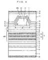
- Fig. 1 is a sectional view of a semiconductor laser device according to the embodiment of the present invention.
- an n-type first buffer layer 2 of n-type GaAs, an n-type second buffer layer 3 of n-type AlGaAs, an n-type cladding layer 4 of n-type AlGaAs, an n-type carrier blocking layer 5 of n-type AlGaAs, a light guide layer 6 of undoped AlGaAs and an active layer 7 of an undoped multiple quantum well structure are successively formed on an n-type semiconductor substrate 1 of n-type GaAs.
- the n-type semiconductor substrate 1 is a slightly inclined substrate having an upper surface inclined from the (100) plane by several degrees (4° in the [011] direction in this embodiment) in the ⁇ 011> direction on the plane.
- the active layer 7 is formed by alternately stacking three quantum well layers 71 of undoped GaAs and two barrier layers 72 of undoped AlGaAs.
- a light guide layer 8 of undoped AlGaAs, a p-type carrier blocking layer 9 of p-type AlGaAs and a p-type first cladding layer 10 of p-type AlGaAs are successively formed on the active layer 7.
- the light guide layer 6, the active layer 7 and the light guide layer 8 form an emission layer 100.
- a striped p-type second cladding layer 12 of p-type AlGaAs extending toward a cavity and a p-type first contact layer 13 of p-type GaAs are successively stacked on a central portion of the p-type first cladding layer 10 through a p-type etching stop layer 11 of p-type AlGaAs to form a ridge portion 200.
- the striped ridge portion 200 extends in the ⁇ 011> direction on the upper surface of the n-type semiconductor substrate 1.
- a first current blocking layer 14 of undoped AlGaAs, an n-type second current blocking layer 15 of n-type AlGaAs and an n-type third current blocking layer 16 of n-type GaAs are successively formed on both side surfaces of the p-type second cladding layer 12 and the p-type first contact layer 13 forming the ridge portion 200 and flat surface portions of the p-type first cladding layer 10 located on both sides of the ridge portion 200.
- a p-type second contact layer 17 of p-type GaAs and a p-type third contact layer 18 of p-type GaAs are successively formed over the p-type first contact layer 13 and the n-type third current blocking layer 16.
- a p-type electrode 19 is formed on the p-type third contact layer 18, and an n-type electrode 20 is formed on the rear surface of the n-type semiconductor substrate 1.
- Figs. 2(a) to 3(d) illustrate a method of manufacturing the semiconductor laser device according to this embodiment.
- the n-type first buffer layer 2, the n-type second buffer layer 3, the n-type cladding layer 4, the n-type carrier blocking layer 5, the light guide layer 6, the active layer 7, the light guide layer 8, the p-type carrier blocking layer 9, the p-type first cladding layer 10, the p-type etching stop layer 11, the p-type second cladding layer 12 and the p-type first contact layer 13 are successively grown on the upper surface of the n-type semiconductor substrate 1 inclined from the (100) plane by several degrees (4° in the [011] direction in this embodiment) in the ⁇ 011> direction on the plane by MOCVD (metal-organic chemical vapor deposition) or MBE (molecular beam epitaxy) at a growth temperature of 700 to 900°C.
- MOCVD metal-organic chemical vapor deposition
- MBE molecular beam epitaxy
- Table 1 shows the materials, Al composition ratios, thicknesses and carrier concentrations of the respective layers 2 to 13.
- the Al composition ratio is expressed by X (the atomic concentration ratio of Al to the sum of the contents of Al and Ga) in Al x Ga 1-x As.
- the carrier concentration of the n-type semiconductor substrate 1 is 2 ⁇ 10 18 cm -3 .
- n-type first buffer layer 2 In order to grow the n-type first buffer layer 2, AsH 3 and TMG are employed as material gas and H 2 Se is employed as dopant gas.
- n-type second buffer layer 3 In order to grow the n-type cladding layer 4 and the n-type carrier blocking layer 5, AsH 3 , TMG and TMA are employed as material gas and H 2 Se is employed as dopant gas.
- AsH 3 , TMG and TMA are employed as material gas.
- the p-type carrier blocking layer 9 In order to grow the p-type carrier blocking layer 9, the p-type first cladding layer 10, the p-type etching stop layer 11 and the p-type second cladding layer 12, AsH 3 , TMG and TMA are employed as material gas and DEZ is employed as dopant gas. In order to grow the p-type first contact layer 13, AsH 3 and TMG are employed as material gas and DEZ is employed as dopant gas.
- AsH 3 stands for arsine
- TMG stands for trimethyl gallium
- TMA stands for trimethyl aluminum
- H 2 Se stands for hydrogen selenide
- SiH 4 stands for monosilane
- DEZ stands for diethylzinc.
- the Al composition ratio in each of the layers 2 to 13 was adjusted by adjusting the ratio of the supply quantities of TMG and TMA.
- the supply quantities of the material gas were controlled with mass flow controllers (MFCS).
- an oxide film of SiO 2 or the like is formed on the p-type first contact layer 13 and thereafter removed by general photolithography while leaving a central striped region, thereby forming a striped oxide film 21 on the p-type first contact layer 13.
- the striped oxide film 21 is formed to extend in the ⁇ 011> direction on the upper surface of the n-type semiconductor substrate 1.
- the p-type first contact layer 13, the p-type second cladding layer 12 and the p-type etching stop layer 11 are removed by etching through the oxide film 21 serving as a mask until the p-type first cladding layer 10 is exposed, as shown in Fig. 2(b).
- the striped ridge portion 200 is formed under the oxide film 21.
- the striped ridge portion 200 extends in the ⁇ 011> direction on the upper surface of the n-type semiconductor substrate 1.
- the layers 13, 12 and 11 may be removed by either wet etching or dry etching.
- the etching stop layer 11 may alternatively be prepared from GaAs, for example, so far as the difference between the Al composition ratios of the etching stop layer 11 and the p-type second cladding layer 12 is in excess of a constant level.
- the angle ⁇ (equal to the angle formed by the side surfaces of the ridge portion 200 and the upper surface of the p-type etching stop layer 11 in this embodiment) of inclination of the side surfaces of the ridge portion 200 with respect to the n-type semiconductor substrate 1 can be set to a prescribed value described below in detail by controlling the relation between the plane orientation of the upper surface of the semiconductor substrate 1 and the striped direction of the ridge portion 200, the contents of hydrogen peroxide and water and the temperature in wet etching or energy of ions in reactive ion etching or reactive ion beam etching.
- the angle ⁇ of inclination on the side surfaces of the ridge portion 200 can be readily set in excess of 70° by selecting the direction of extension of the striped oxide film 21 along the ⁇ 011> direction.
- the angle ⁇ of inclination on the side surfaces of the ridge portion 200 can be readily set in excess of 70° regardless of the direction of extension of the oxide film 21.
- the angle ⁇ of inclination on the side surfaces of the ridge portion 200 can be set in excess of 70° under conditions not damaging the etching surface by selecting the direction of extension of the striped oxide film 21 along the ⁇ 011> direction.
- a lower width W of the ridge portion 200 can be set to a prescribed value described below in detail by controlling the thickness of the p-type second cladding layer 12, the width of the oxide film 21, the angle ⁇ of inclination on the side surfaces of the ridge portion 200, the etching time or the like.
- the sum of the thicknesses of the p-type carrier blocking layer 9 and the p-type first cladding layer 10 is set to a prescribed value described below in detail by controlling the growth times for forming the p-type carrier blocking layer 9 and the p-type first cladding layer 10 in the step shown in Fig. 2(a) and controlling the etching depth by the etching stop layer 11 in the step shown in Fig. 2(b).
- the sum of the thicknesses of the p-type carrier blocking layer 9 and the p-type first cladding layer 10 defines the distance t between the emission layer 100 and the first current blocking layer 14 formed in a subsequent step.
- the undoped first current blocking layer 14, the n-type second current blocking layer 15 and the n-type third current blocking layer 16 are selectively grown on the flat surface portions located on both sides of the ridge portion 200 and the side surfaces of the rid°ge portion 200 through the oxide film 21 serving as a mask at a growth temperature of 600 to 900°. At this time, these layers 14 and 16 are not gown on the oxide film 21.
- Table 2 shows the material, Al composition ratios, thicknesses and carrier concentrations of the layers 14 and 16.
- the A1 composition ratio of the first current blocking layer 14 is set in a range satisfying conditions described below in detail.
- TMG and TMA are employed as material gas.
- AsH 3 TMG and TMA are employed as material gas and H 2 Se is employed as dopant gas.
- AsH 3 and TMG are employed as material gas and H 2 Se is employed as dopant gas.
- the Al composition ratios are adjusted by adjusting the ratios of the supply quantities of TMG and TMA, similarly to the case of the aforementioned layers 2 to 13.
- Table 3 shows the materials, Al composition ratios, thicknesses and carrier concentrations of the layers 17 and 18.
- Table 3 Material A1 Composition Ratio (Atomic Concentration Ratio) Thickness ( ⁇ m) Carrier Concentration (cm -3 ) p-Type Second Contact Layer 17 GaAs 0 5.3 1 ⁇ 10 19 p-Type Third Contact Layer 18 GaAs 0 0.7 6 ⁇ 10 19
- the thickness of the p-type first contact layer 13, which can be remarkably reduced without causing any problem on the characteristics of the device, may be in the range of at least 5 nm and not more than 1000 nm.
- the p-type electrode 19 of CrAu in a thickness of about 50 nm and Au in a thickness of about 1.5 ⁇ m is formed on the p-type third contact layer 18 while the n-type electrode 20 of AuGe/Ni/Au is formed on the rear surface of the n-type semiconductor substrate 1.
- the semiconductor laser device having the structure shown in Fig. 1 is manufactured through the aforementioned steps.
- a plurality of types of samples were prepared by setting the angle ⁇ (corresponding to the angle ⁇ formed by the side surfaces of the ridge portion 200 and the upper surface of the etching stop layer 11 in this embodiment) at 55°, 70°, 80°, 90°, 100°, 110°, 117° and 125° respectively.
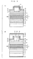
- Each sample of the semiconductor laser device had the ridge portion 200 of the forward mesa structure shown in Fig. 4 when the angle ⁇ of inclination was set to 55°, 70° and 80°, while each sample of the semiconductor laser device had the ridge portion 200 of the reverse mesa structure shown in Fig.
- the angle ⁇ of inclination was measured by observing the front facet of each sample with a scanning electron microscope (SEM) after preparation of the sample and acquiring a sectional SEM image (photograph) of the front facet. At this time, the magnification was set to about 6000. The angle formed by the side walls of the ridge portion 200 and the flat portion was measured with a protractor on the obtained SEM image (photograph), to obtain the angle ⁇ of inclination.
- SEM scanning electron microscope
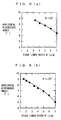
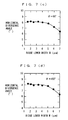
- the lower widths W of the ridge portions 200 were varied for measuring the horizontal divergence angles of the laser beams.
- Figs. 6(a) to 7(f) show the results.
- the thickness of the p-type second cladding layer 12 was 2000 nm.
- the semiconductor laser device having the ridge portion 200 of the reverse mesa structure with the angle ⁇ of inclination of 100° and the lower width W of 4 ⁇ m shown in Fig. 5 four types of samples were prepared by setting the Al composition ratio X2 of the first current blocking layer 14 and the n-type second current blocking layer 15 to 0.55, 0.62, 0.75 and 0.80 respectively, for investigating the relation between the distance t between the emission layer 100 and the first current blocking layer 14 (the sum of the thicknesses of the n-type carrier blocking layer 9 and the p-type first cladding layer 10) and the horizontal divergence angle of the laser beam in each sample.
- Fig. 8 shows the results.
- the horizontal divergence angle of the laser beam is reduced when the distance t is increased, while inclination of such reduction of the horizontal divergence angle is reduced when the distance t exceeds 0.15 ⁇ m and the inclination of the reduction of the horizontal divergence angle is further reduced when the distance t exceeds 0.2 ⁇ m.
- This first critical distance t1 is 0.31 when the Al composition ratio X2 is 0.55, 0.33 when the Al composition ratio X2 is 0.62, 0.39 when the Al composition ratio X2 is 0.75, and 0.42 when the Al composition ratio X2 is 0.80.
- the second critical distance t2 is 0.28 when the Al composition ratio X2 is 0.55, 0.31 when the Al composition ratio X2 is 0.62, 0.36 when the Al composition ratio X2 is 0.75, and 0.39 when the Al composition ratio X2 is 0.80.
- t1 0.275/(1 - (X2 - X1)).
- the horizontal divergence angle is abruptly reduced when the distance t exceeds 0.275/(1 - (X2 - X1)), and hence the distance t must satisfy the relation of t ⁇ 0.275/(1 - (X2 - X1) ) in order not to abruptly reduce the horizontal divergence angle.
- the distance t must satisfy the relation of t ⁇ 0.275/(1 - (X2 - X1)) in order not to abruptly reduce the horizontal divergence angle also when setting the angle ⁇ of inclination to 70°, 80°, 110° and 117°.
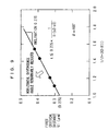
- the horizontal divergence angle of the laser beam is substantially constant when the lower width W of the ridge portion 200 is at least 1.5 ⁇ m and not more than 5 ⁇ m, while the horizontal divergence angle of the laser beam is abruptly reduced when the lower width W exceeds 5 ⁇ m.
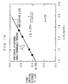
- the operating voltage is abruptly increased when the lower width W of the ridge portion 200 falls below 2 ⁇ m. Therefore, the lower width W must be at least 2 ⁇ m.
- the lower width W of the ridge portion 200 is preferably at least 2 ⁇ m and not more than 5 ⁇ m in consideration of the horizontal divergence angle and the operating voltage, as understood from Figs. 14 and 15.
- the distance t must satisfy the relation of t ⁇ 0.252/(1 - (X2 - X1)) in order to attain a horizontal divergence angle (at least 5° in this embodiment) exceeding a constant value with small reduction. Similar results were obtained also when setting the angle ⁇ of inclination on the side surfaces of the ridge portion 200 to 70°, 80°, 110° and 117°.
- the first and second cladding layers 10 and 12 may alternatively have different Al composition ratios.
- the second cladding layer 12 forming the ridge portion 200 has the Al composition ratio X1.
- n-type semiconductor substrate 1 is formed by the slightly inclined substrate having the upper surface inclined by 4° from the (100) plane in the ⁇ 011> direction on the plane, results similar to those of the aforementioned embodiment were obtained when the angle of inclination was at least 0° and not more than 13°.
- the upper surface may be the ⁇ 100 ⁇ plane including the (100) plane or may be inclined by several degrees from the ⁇ 100 ⁇ plane, and the striped ridge portion 200 may extend in the ⁇ 011> direction in this case.
- a striped mask extending in the ⁇ 011> direction may be prepared.
- the upper surface may be the ⁇ 1 00 ⁇ plane or may be inclined by several degrees from the ⁇ 1 00 ⁇ plane, and the striped ridge portion 200 may extend in the ⁇ 011> direction in this case.
- a striped mask extending in the ⁇ 011> direction may be prepared.
- the semiconductor laser device contains Al and Ga as the group III elements in the aforementioned embodiment, the present invention is also applicable to a semiconductor laser device containing another group III element such as In. The present invention is further applicable to a semiconductor laser device containing P, N and the like as group V elements other than As.
- a method of manufacturing a semiconductor laser device which can readily manufacture a semiconductor laser device capable of suppressing reduction of a horizontal divergence angle of a laser beam and readily adjusting the horizontal divergence angle of the laser beam also when increasing the output of the laser beam.
Landscapes
- Physics & Mathematics (AREA)
- Geometry (AREA)
- Condensed Matter Physics & Semiconductors (AREA)
- General Physics & Mathematics (AREA)
- Electromagnetism (AREA)
- Optics & Photonics (AREA)
- Semiconductor Lasers (AREA)
Claims (16)
- Dispositif laser à semi-conducteur comprenant:un substrat (1);une première couche de revêtement de type deconductivité (4);une couche d'émission (100);une seconde couche de revêtement de type de conductivité (10) contenant du Al en tant qu'élément du groupe III et formée avec une partie de saillie (11, 12) ; etune couche de blocage de courant (14), formée sur ladite seconde couche de revêtement de type de conductivité autour (10) de ladite partie de saillie (11, 12), contenant du Al en tant qu'élément du groupe III dans cet ordre, dans lequelun angle θ d'inclinaison sur les surfaces latérales de ladite partie de saillie (11, 12) par rapport à la surface supérieure dudit substrat (1) est d'au moins 70° et de pas plus de 117°,une largeur inférieure W de ladite partie de saillie (11, 12) est d'au moins 2 µm et de pas plus de 5 µm,caractérisé en ce que:ladite couche d'émission (100) comprend une couche active (7) et une couche de guidage de lumière (8);une seconde couche de blocage de porteur de type de conductivité (9) est formée sur la couche de guidage de lumière (8); etla distance t entre ladite couche d'émission (100) et ladite couche de blocage d u courant électrique (14) correspond à l'épaisseur de ladite seconde couche de blocage de porteur de type de conductivité (9) et a l'épaisseur de ladite seconde couche de revêtement de type de conductivité (10) à l'exclusion de la partie de saillie (11, 12) et satisfait la relation de t ≤ 0,275/(1 - (X2 - X1)) [µm] en supposant que X1 représente le rapport de composition de Al dans les éléments du groupe III formant ladite seconde couche de revêtement de type de conductivité (10), X2 représente le rapport de composition de Al dans les éléments du groupe III formant ladite couche de blocage (14).
- Dispositif laser à semi-conducteur selon la revendication 1, dans lequel
ladite seconde couche de revêtement de type de conductivité (10) contient du Al et du Ga en tant qu'éléments du groupe III, et X1 représente le rapport de composition de Al dans la somme des teneurs en Al et en Ga, et
ladite couche de blocage (14) contient du Al et du Ga en tant qu'éléments du groupe III, et X2 représente le rapport de composition de Al dans la somme des teneurs en Al et en Ga. - Dispositif laser à semi-conducteur selon la revendication 2, dans lequel
ladite seconde couche de revêtement de type de conductivité (10) est constituée de Alx1Ga1-x1As, et
ladite couche de blocage (14) est constituée de Alx2Ga1-x2As. - Dispositif laser à semi-conducteur selon la revendication 1, dans lequel
ladite distance t satisfait la relation de t ≤ 0,252/(1 - (X2 - X1)) [µm]. - Dispositif laser à semi-conducteur selon la revendication 1, dans lequel
ladite distance t est d'au moins 0,15 µm. - Dispositif laser à semi-conducteur selon la revendication 1, dans lequel
ladite distance t est d'au moins 0,2 µm. - Dispositif laser à semi-conducteur selon la revendication 1, dans lequel
la surface supérieure dudit substrat (1) est le plan {100} ou est inclinée de plusieurs degrés à partir du plan {100}, et ladite partie de saillie (11, 12) s'étend dans la direction <011>. - Dispositif laser à semi-conducteur selon la revendication 1, dans lequel
la surface supérieure dudit substrat (1) est le plan {100} ou inclinée de plusieurs degrés à partir du plan {100}, et ladite partie de saillie s'étend dans la direction <011>. - Procédé de fabrication d'un dispositif laser à semi-conducteur comprenant les étapes consistant à:former une première couche de revêtement de type de conductivité (4), une couche d'émission (100), une seconde couche de revêtement de type de conductivité (10) ayant une épaisseur prescrite, une couche d'arrêt d'attaque chimique et une seconde couche de revêtement de type de conductivité (12) ayant un rapport de composition X1 de Al dans les éléments du groupe III sur un substrat (1) dans cet ordre;retirer partiellement ladite seconde couche de revêtement de type de conductivité (12) en formant ainsi une partie de saillie (11, 12) ayant un angle θ d'inclinaison d'au moins 70° et de pas plus de 117° sur les surfaces latérales par rapport à la surface supérieure dudit substrat (1) et une largeur W d'au moins 2 µm et de pas plus de 5 µm; etformer une couche de blocage de courant (14) sur les deux côtés de ladite partie de saillie (11, 12) ; caractérisé en ce que:ladite couche d'émission (100) comprend une couche active (7) et une couche de guidage de lumière (8);le procédé comprend la formation d'une seconde couche de blocage de porteur de type de conductivité (9) sur la couche de guidage de lumière (8); etla distance t entre ladite couche d'émission (100) et ladite couche de courant (14) correspond à l'épaisseur ladite seconde couche de porteur de type de conductivité (9) et à l'épaisseur de ladite seconde couche de revêtement de type de conductivité (10) et satisfait la relation de t ≤ 0,275/(1 - (X2 - X1)) [µm] en supposant que X1 représente le rapport de composition de Al dans les éléments du groupe III formant ladite seconde couche de revêtement de type de conductivité (10), X2 représente le rapport de composition de Al dans les éléments du groupe III formant ladite couche de blocage de courant (14).
- Procédé de fabrication d'un dispositif laser à semi-conducteur selon la revendication 9, dans lequel
lesdites secondes couches de premier et second revêtements de type de conductivité (10) contiennent du Al et du Ga en tant qu'éléments du groupe III, et X1 représente le rapport de composition de Al dans la somme des teneurs en Al et en Ga, et
ladite couche de blocage (14) contient du Al et du Ga en tant qu'éléments du groupe III, et X2 représente le rapport de composition de Al dans la somme des teneurs en Al et en Ga. - Procédé de fabrication d'un dispositif laser à semi-conducteur selon la revendication 10, dans lequel
lesdites secondes couches de premier et second revêtements de type de conductivité (10, 12) sont constituées de Alx1Ga1-x1As, et
ladite couche de blocage (14) est constituée de Alx2Ga1-x2As. - Procédé de fabrication d'un dispositif laser à semi-conducteur selon la revendication 9, dans lequel
ladite distance t satisfait la relation de t ≤ 0,252/(1 - (X2 - X1)) [µm]. - Procédé de fabrication d'un dispositif laser à semi-conducteur selon la revendication 9, dans lequel
ladite distance t est d'au moins 0,15 µm. - Procédé de fabrication d'un dispositif laser à semi-conducteur selon la revendication 9, dans lequel
ladite distance t est d'au moins 0,2 µm. - Procédé de fabrication d'un dispositif laser à semi-conducteur selon la revendication 9, dans lequel
la surface supérieure dudit substrat (1) est le plan {100} ou est inclinée de plusieurs degrés à partir du plan {100}, et
ladite étape consistant à former de ladite partie de saillie (11, 12) comprend les étapes consistant à former d'un masque (21) s'étendant dans la direction <011> et à réaliser une attaque chimique avec ledit masque (21). - Procédé de fabrication d'un dispositif laser à semi-conducteur selon la revendication 9, dans lequel
la surface supérieure dudit substrat (1) est le plan {100} ou est inclinée de plusieurs degrés à partir du plan {100}, et
ladite étape consistant à former ladite partie de saillie (11, 12) comprend les étapes consistant à former un masque (21) s'étendant dans la direction < 011> et de réalisation d'une attaque chimique avec ledit masque (21).
Applications Claiming Priority (4)
| Application Number | Priority Date | Filing Date | Title |
|---|---|---|---|
| JP27243699 | 1999-09-27 | ||
| JP27243699 | 1999-09-27 | ||
| JP2000012681 | 2000-01-21 | ||
| JP2000012681 | 2000-01-21 |
Publications (3)
| Publication Number | Publication Date |
|---|---|
| EP1087480A2 EP1087480A2 (fr) | 2001-03-28 |
| EP1087480A3 EP1087480A3 (fr) | 2003-10-08 |
| EP1087480B1 true EP1087480B1 (fr) | 2006-11-15 |
Family
ID=26550201
Family Applications (1)
| Application Number | Title | Priority Date | Filing Date |
|---|---|---|---|
| EP00308345A Expired - Lifetime EP1087480B1 (fr) | 1999-09-27 | 2000-09-22 | Dispositif laser à semiconducteur et méthode de fabrication |
Country Status (5)
| Country | Link |
|---|---|
| US (1) | US6891872B1 (fr) |
| EP (1) | EP1087480B1 (fr) |
| KR (1) | KR100798170B1 (fr) |
| CN (1) | CN1290055A (fr) |
| DE (1) | DE60031819T2 (fr) |
Families Citing this family (5)
| Publication number | Priority date | Publication date | Assignee | Title |
|---|---|---|---|---|
| JP2002374040A (ja) * | 2001-06-15 | 2002-12-26 | Sharp Corp | 半導体レーザ素子およびその製造方法 |
| JP2003273467A (ja) | 2002-03-15 | 2003-09-26 | Toshiba Corp | 半導体レーザおよびその製造方法 |
| JP2006179565A (ja) * | 2004-12-21 | 2006-07-06 | Sony Corp | 半導体レーザ素子 |
| JP2009059933A (ja) * | 2007-08-31 | 2009-03-19 | Toshiba Corp | 半導体発光素子 |
| KR102440071B1 (ko) * | 2020-10-16 | 2022-09-05 | (주)큐에스아이 | 반도체 레이저 다이오드 소자 및 그 제조 방법 |
Family Cites Families (16)
| Publication number | Priority date | Publication date | Assignee | Title |
|---|---|---|---|---|
| JPH0770779B2 (ja) | 1985-09-04 | 1995-07-31 | 株式会社日立製作所 | 半導体レーザの製造方法 |
| DE69033518T2 (de) * | 1989-07-12 | 2000-12-21 | Kabushiki Kaisha Toshiba, Kawasaki | Im transversalen Mode schwingender Halbleiterlaser |
| JP2778178B2 (ja) * | 1990-01-31 | 1998-07-23 | 日本電気株式会社 | 半導体レーザ |
| JP3154198B2 (ja) | 1992-08-25 | 2001-04-09 | ソニー株式会社 | 半導体レーザとその製法 |
| CA2138912C (fr) | 1993-12-24 | 1999-05-04 | Shoji Ishizaka | Laser a semiconducteur |
| JP3322512B2 (ja) * | 1994-04-28 | 2002-09-09 | 三洋電機株式会社 | 半導体レーザ素子の設計方法 |
| TW291585B (fr) * | 1994-07-04 | 1996-11-21 | Mitsubishi Chem Corp | |
| JPH09116222A (ja) | 1995-10-17 | 1997-05-02 | Mitsubishi Electric Corp | 半導体レーザの製造方法,及び半導体レーザ |
| JP3199158B2 (ja) * | 1995-12-26 | 2001-08-13 | シャープ株式会社 | 半導体レーザ装置 |
| JP3429407B2 (ja) * | 1996-01-19 | 2003-07-22 | シャープ株式会社 | 半導体レーザ装置およびその製造方法 |
| US5968845A (en) * | 1996-02-13 | 1999-10-19 | Matsushita Electric Industrial Co., Ltd. | Method for etching a compound semiconductor, a semi-conductor laser device and method for producing the same |
| US6118800A (en) * | 1996-03-01 | 2000-09-12 | Matsushita Electric Industrial Co., Ltd. | Semiconductor laser and cleaving method |
| TW342545B (en) * | 1996-03-28 | 1998-10-11 | Sanyo Electric Co | Semiconductor laser element and method for designing same |
| JP2674592B2 (ja) | 1996-04-22 | 1997-11-12 | 株式会社日立製作所 | 半導体レーザ |
| JPH11163458A (ja) | 1997-11-26 | 1999-06-18 | Mitsui Chem Inc | 半導体レーザ装置 |
| JP2000101200A (ja) * | 1998-09-25 | 2000-04-07 | Sony Corp | 半導体レーザーおよびマルチ半導体レーザー |
-
2000
- 2000-09-22 EP EP00308345A patent/EP1087480B1/fr not_active Expired - Lifetime
- 2000-09-22 DE DE60031819T patent/DE60031819T2/de not_active Expired - Lifetime
- 2000-09-25 US US09/669,448 patent/US6891872B1/en not_active Expired - Fee Related
- 2000-09-26 KR KR1020000056350A patent/KR100798170B1/ko not_active Expired - Fee Related
- 2000-09-27 CN CN00130582A patent/CN1290055A/zh active Pending
Also Published As
| Publication number | Publication date |
|---|---|
| KR100798170B1 (ko) | 2008-01-24 |
| EP1087480A3 (fr) | 2003-10-08 |
| DE60031819D1 (de) | 2006-12-28 |
| EP1087480A2 (fr) | 2001-03-28 |
| US6891872B1 (en) | 2005-05-10 |
| DE60031819T2 (de) | 2007-09-13 |
| CN1290055A (zh) | 2001-04-04 |
| KR20010030489A (ko) | 2001-04-16 |
Similar Documents
| Publication | Publication Date | Title |
|---|---|---|
| US7554127B2 (en) | Semiconductor light-emitting element and method of manufacturing the same | |
| US5889805A (en) | Low-threshold high-efficiency laser diodes with aluminum-free active region | |
| US20080137701A1 (en) | Gallium Nitride Based Semiconductor Device with Reduced Stress Electron Blocking Layer | |
| US5929462A (en) | Semiconductor optical device having a strained quantum well structure | |
| EP0661784B1 (fr) | Laser à diode à semi-conducteur | |
| EP0325275A2 (fr) | Laser à semi-conducteur pour l'émission de lumière avec des couches cristallines à (AlxGa1-x)0.5In0.5P et procédé pour la croissance d'un cristal à (AlxGa1-x)0,5In0.5P | |
| EP1024566B1 (fr) | Laser à semi-conducteur et son procédé de fabrication | |
| US7804869B2 (en) | Gallium nitride based semiconductor device with electron blocking layer | |
| EP1006629A2 (fr) | Dispositif émetteur de lumière à semi-conducteur composé | |
| EP1087480B1 (fr) | Dispositif laser à semiconducteur et méthode de fabrication | |
| US5574741A (en) | Semiconductor laser with superlattice cladding layer | |
| US7495262B2 (en) | Compound semiconductor, method for producing the same, semiconductor light-emitting device and method for fabricating the same | |
| US5270246A (en) | Manufacturing method of semiconductor multi-layer film and semiconductor laser | |
| US7590158B2 (en) | Semiconductor laser having an improved window layer and method for the same | |
| EP0952645B1 (fr) | Dispositif laser à semi-conducteur | |
| US7215691B2 (en) | Semiconductor laser device and method for fabricating the same | |
| JP4030260B2 (ja) | 半導体レーザ素子及びその製造方法 | |
| EP1104947A2 (fr) | Laser à semiconducteur à Nitrure et méthode de fabrication | |
| US20030118069A1 (en) | Vertical cavity surface emitting laser including indium in the active region | |
| US7072371B2 (en) | Ridge-type semiconductor laser element fabrication method | |
| JP3239821B2 (ja) | 歪み半導体結晶の製造方法 | |
| US20030118068A1 (en) | Vertical cavity surface emitting laser including indium and nitrogen in the active region | |
| US5151912A (en) | Semiconductor laser | |
| JPH11340585A (ja) | 半導体発光装置 | |
| JP3658229B2 (ja) | 半導体レーザ素子及びその製造方法 |
Legal Events
| Date | Code | Title | Description |
|---|---|---|---|
| PUAI | Public reference made under article 153(3) epc to a published international application that has entered the european phase |
Free format text: ORIGINAL CODE: 0009012 |
|
| AK | Designated contracting states |
Kind code of ref document: A2 Designated state(s): AT BE CH CY DE DK ES FI FR GB GR IE IT LI LU MC NL PT SE |
|
| AX | Request for extension of the european patent |
Free format text: AL;LT;LV;MK;RO;SI |
|
| PUAL | Search report despatched |
Free format text: ORIGINAL CODE: 0009013 |
|
| AK | Designated contracting states |
Kind code of ref document: A3 Designated state(s): AT BE CH CY DE DK ES FI FR GB GR IE IT LI LU MC NL PT SE |
|
| AX | Request for extension of the european patent |
Extension state: AL LT LV MK RO SI |
|
| 17P | Request for examination filed |
Effective date: 20040401 |
|
| AKX | Designation fees paid |
Designated state(s): DE FR GB NL |
|
| 17Q | First examination report despatched |
Effective date: 20041015 |
|
| GRAP | Despatch of communication of intention to grant a patent |
Free format text: ORIGINAL CODE: EPIDOSNIGR1 |
|
| GRAS | Grant fee paid |
Free format text: ORIGINAL CODE: EPIDOSNIGR3 |
|
| GRAA | (expected) grant |
Free format text: ORIGINAL CODE: 0009210 |
|
| AK | Designated contracting states |
Kind code of ref document: B1 Designated state(s): DE FR GB NL |
|
| REG | Reference to a national code |
Ref country code: GB Ref legal event code: FG4D |
|
| REF | Corresponds to: |
Ref document number: 60031819 Country of ref document: DE Date of ref document: 20061228 Kind code of ref document: P |
|
| ET | Fr: translation filed | ||
| PLBE | No opposition filed within time limit |
Free format text: ORIGINAL CODE: 0009261 |
|
| STAA | Information on the status of an ep patent application or granted ep patent |
Free format text: STATUS: NO OPPOSITION FILED WITHIN TIME LIMIT |
|
| 26N | No opposition filed |
Effective date: 20070817 |
|
| PGFP | Annual fee paid to national office [announced via postgrant information from national office to epo] |
Ref country code: GB Payment date: 20090916 Year of fee payment: 10 Ref country code: NL Payment date: 20090915 Year of fee payment: 10 |
|
| PGFP | Annual fee paid to national office [announced via postgrant information from national office to epo] |
Ref country code: FR Payment date: 20091012 Year of fee payment: 10 |
|
| PGFP | Annual fee paid to national office [announced via postgrant information from national office to epo] |
Ref country code: DE Payment date: 20100915 Year of fee payment: 11 |
|
| REG | Reference to a national code |
Ref country code: NL Ref legal event code: V1 Effective date: 20110401 |
|
| GBPC | Gb: european patent ceased through non-payment of renewal fee |
Effective date: 20100922 |
|
| REG | Reference to a national code |
Ref country code: FR Ref legal event code: ST Effective date: 20110531 |
|
| PG25 | Lapsed in a contracting state [announced via postgrant information from national office to epo] |
Ref country code: FR Free format text: LAPSE BECAUSE OF NON-PAYMENT OF DUE FEES Effective date: 20100930 |
|
| PG25 | Lapsed in a contracting state [announced via postgrant information from national office to epo] |
Ref country code: NL Free format text: LAPSE BECAUSE OF NON-PAYMENT OF DUE FEES Effective date: 20110401 Ref country code: GB Free format text: LAPSE BECAUSE OF NON-PAYMENT OF DUE FEES Effective date: 20100922 |
|
| REG | Reference to a national code |
Ref country code: DE Ref legal event code: R119 Ref document number: 60031819 Country of ref document: DE Effective date: 20130403 |
|
| PG25 | Lapsed in a contracting state [announced via postgrant information from national office to epo] |
Ref country code: DE Free format text: LAPSE BECAUSE OF NON-PAYMENT OF DUE FEES Effective date: 20130403 |