EP0920103A1 - System zur Versorgung einer reaktiven Last - Google Patents
System zur Versorgung einer reaktiven Last Download PDFInfo
- Publication number
- EP0920103A1 EP0920103A1 EP97830628A EP97830628A EP0920103A1 EP 0920103 A1 EP0920103 A1 EP 0920103A1 EP 97830628 A EP97830628 A EP 97830628A EP 97830628 A EP97830628 A EP 97830628A EP 0920103 A1 EP0920103 A1 EP 0920103A1
- Authority
- EP
- European Patent Office
- Prior art keywords
- load
- supply
- current
- electrical quantity
- electronic switch
- Prior art date
- Legal status (The legal status is an assumption and is not a legal conclusion. Google has not performed a legal analysis and makes no representation as to the accuracy of the status listed.)
- Granted
Links
Images

Classifications
-
- H—ELECTRICITY
- H05—ELECTRIC TECHNIQUES NOT OTHERWISE PROVIDED FOR
- H05B—ELECTRIC HEATING; ELECTRIC LIGHT SOURCES NOT OTHERWISE PROVIDED FOR; CIRCUIT ARRANGEMENTS FOR ELECTRIC LIGHT SOURCES, IN GENERAL
- H05B44/00—Circuit arrangements for operating electroluminescent light sources
Definitions
- the present invention relates to a system for driving a reactive load as defined in the preamble of Claim 1.
- An amplifier 1 has an output stage represented schematically by two controllable current sources G1, G2, connected in series between the rails of a voltage supply, indicated Vs and by the earth symbol.
- the output terminal of the amplifier which is the connection node between the two current sources is connected to a capacitive load represented by a capacitor Cl.
- a control circuit 2 supplies control signals to the amplifier so as to modulate the supply or absorption of current by the current sources G1 and G2, and hence the supply to the load Cl, in accordance with a predetermined program.
- a capacitive load for example, a piezoelectric printing head of an ink-jet printer or an element of an electroluminescent panel, again indicated Cl, is connected to the output of an operational amplifier 3 having an output stage represented by two controllable current sources G1 and G2 connected in series with one another between the terminals Vs and earth of a direct-current voltage supply, as in the system of Figure 1.
- an operational amplifier 3 having an output stage represented by two controllable current sources G1 and G2 connected in series with one another between the terminals Vs and earth of a direct-current voltage supply, as in the system of Figure 1.
- an inductance Lr an electronic switch T3 for example, a transistor, and a capacitor Cr, connected in series.
- An activation unit 10 is connected to the control terminal of the electronic switch T3 in order to open it or close it at predetermined time intervals, as will be explained further below.
- the operational amplifier 3 has an inverting input connected to a sensor 12 for detecting an electrical quantity in the load and a non-inverting input connected to a digital-analogue convertor or DAC 16.
- the sensor is a resistive divider connected in parallel with the load Cl and formed by two resistors R1 and R2.
- the intermediate tap of the divider is connected to the inverting input of the amplifier 3 in order to supply a voltage thereto, as the electrical quantity indicative of the operation of the resonant circuit.
- the DAC 16 also supplies to the amplifier 3 a voltage, more precisely, a voltage which varies as the waveform to be produced in the load Cl.
- the operational amplifier operates as a comparator of the voltages applied to its inputs and, together with the sensor 12, constitutes a system with error-compensation feedback.
- the waveform is stored in digital form in a control unit 14 which has the function of coordinating the operation of the system in accordance with a predetermined program.
- it is connected to the activation unit 10 in order to provide it with the control signals for the switch T3 at predetermined times correlated with the waveform stored, for example, as a result of the recognition, in the control unit 14, of a sample of the waveform stored which defines a reference moment.
- control unit 14 is formed in a manner such that the waveform stored and the operating program of the system can be modified according to requirements by means of an input unit 15. In other applications, however, it may suffice for the control unit 14 to contain a non-modifiable waveform and a fixed operating program.
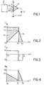
- Figure 6 shows a resonant circuit constituted by the same components Cr, Cl, Lr and T3 which are present in the circuit of Figure 5. It is assumed that the capacitor Cr is charged to a predetermined voltage and that, at the time t0, the switch T3 which, up to this time has been open, is closed. A sinusoidal current Ir which mirrors the exchange of energy between the inductance Lr and the capacitance of the two capacitive components Cr and Cl flows in the resonant circuit, as shown in Figure 7, and is damped over time because of the internal resistance of the circuit.
- the energy stored in the reactive components of the resonant circuit is used, in combination with that supplied or absorbed by the current sources G1 and G2 of the operational amplifier 3, to produce a predetermined waveform in the capacitive load Cl.
- the waveform in the time interval t0-t1 corresponding to one half period of the sinusoidal current Ir, the waveform is required to be a slope like that of Figure 2 in the same period t0-t1.
- the first half-wave of the current of Figure 7 is therefore "squared" in order to become identical to that of Figure 3 between t0 and t1.
- This "squaring" operation can be represented geometrically with reference to Figure 8, if the current in the capacitive load Cl is controlled by means of the operational amplifier 3 in a manner such as to "take away" the top portion of the half-wave, that is, the portion indicated A- in which Ir is greater than I1 and to "add” to the sides of the half-wave, the substantially triangular portions, indicated A+, which are lacking, in order to produce a square wave of amplitude I1.
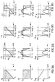
- This operation is performed by the system according to the invention shown in Figure 5 under the control of the control unit 14. More particularly, by enabling the activation unit 10, the control unit 14 causes the switch T3 to be closed and applies a reference voltage to the non-inverting input of the operational amplifier 3 by means of the DAC 16. Upon the assumption that the capacitor Cr is already charged, a current due to the operational amplifier 3 and to the energy exchange between the reactive components of the resonant circuit flows in the capacitive load and a corresponding voltage is detected by the sensor 12. The operational amplifier 3 compares this voltage with the reference voltage supplied by the DAC 16.
- the amplifier 3 supplies the quantity of current which is lacking in order to reach the level I1, by means of the current source G1. As soon as the current in the resonant circuit tends to exceed the value I1 at the time t11, the operational amplifier 3 absorbs the quantity of current in excess of the value I1 by means of the current source G2, discharging it to earth until the time t12.
- the operation of the operational amplifier 3 is similar to that in the period from t0 to t11.
- the activation unit 10 opens the switch T3. Since the time t1 corresponds to the zero-crossing of the current Ir, the activation unit 10 advantageously performs this operation automatically by means of a zero-crossing detector, as shown in Figure 10, which will be described below.
- the area AP between the straight line which represents the power dissipated Pd and the coordinate axes is proportional to that AV defined between the straight line which represents the voltage V and the supply-voltage level Vs.
- the power dissipated at the time t0 is equal to that dissipated at the time t0 in the known system, but decreases rapidly, since it also benefits from the contribution of the current circulating in the resonant circuit, until it reaches zero at the time t11 when the current Ir in the resonant circuit reaches the level I1 necessary to achieve the desired voltage slope in Cl.
- the capacitive load can be discharged in controlled manner, possibly after a waiting period.
- the discharge of the capacitive load can be controlled by the control unit 14 and by the activation unit 10 by a process similar to the charging process, so as to achieve, in the load, a waveform of opposite sign which may be the same as the charging waveform or different, according to the programming of the control unit 14.
- the charging and discharging process, with any intervals, can then be continued in accordance with the program of the control unit 14.
- a phase shift is created between the current Ir circulating in the resonant circuit and the charging or discharging current in the capacitive load Cl. This is achieved by delaying or advancing the closure of the switch T3 relative to a predetermined moment within the period of the waveform, according to the waveform to be reproduced in the capacitive load Cl. This phase shift is achieved by means of a suitable delay unit ⁇ t in the control unit 14.
- the phase shift is an advance, the effect of which can be appreciated from a comparison of Figures 9B and 9C.
- the voltage graph of Figure 9B of the voltage contribution to the power dissipated Pd, expressed graphically by the area AV1, in the period in which the current source G1 supplies current before the time t11, is considerable and is greater than that, expressed by the area AV2, in the period following the time t12 in which the current source G1 supplies current current again.
- a small advance ⁇ t in the closure of T3 reduces the both the voltage and the current contributions in the period t0-t11 so that the net result is a reduction in the mean power dissipated.
- a further reduction in the mean power dissipated is achieved by reducing the supply voltage of the operational amplifier 3 during the period of time in which the voltage in the capacitive load is low, for example, by changing from a level Vs to a level Vs/2, as shown in Figure 9D.
- the contribution of the voltage to the determination of the power in the period of the initial charging of Cl is further reduced in this case. This effect is achieved by means of a suitable supply with two switchable voltage levels.
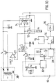
- a schematic example of a supply of this type is shown in Figure 10.
- a voltage supply 38 with two output levels is connected to the supply terminals of the operational amplifier 3 in parallel with a smoothing capacitor C.
- An electronic switch T4 is associated with the supply 38 and is controlled by the output of a comparator 37.
- the latter has one input connected to a reference supply VREF and the other input connected to the sensor 12.
- VREF reference supply
- the output of the comparator is at a low level, that is, such as not to activate the switch T4 and the operational amplifier 3 is supplied by the lower-level voltage.
- the output of the comparator 37 is at a high level such as to close the switch T4 so that the operational amplifier 3 is supplied with the higher-level voltage. Since, as can be seen in the voltage graph of Figure 9D, the contribution of the voltage to the power dissipated is reduced in the period in which the current source G1 supplies current for the initial charging of the load Cl, the power dissipated in this period of time is also reduced.
- FIG. 10 also shows in some detail the unit 10 for activating the switch T3.
- This unit 10 comprises a flip-flop 30 an input S of which receives a switching (setting) signal from a counter 33 connected to the control unit 14. The time at which this signal is emitted is determined by the control unit 14 on the basis of the wave-form programmed to be reproduced in the capacitive load and on the basis of any delay or advance ⁇ t programmed.
- the setting signal at the input S of the flip-flop produces a "high" signal at the output Q of the flip-flop such as to close the switch T3.
- the counting cycle of the counter is selected so as to define the most suitable moment to close the switch T3 within the period of the waveform.
- the activation unit 10 also comprises a current zero-crossing detector 32 comprising a capacitor Co and a resistor Ro connected in series with one another in parallel with the capacitor Cr of the resonant circuit, as well as two diodes connected so as to conduct in opposite directions in parallel with the resistor Ro, in order to limit the voltage drop therein.
- a current zero-crossing detector 32 comprising a capacitor Co and a resistor Ro connected in series with one another in parallel with the capacitor Cr of the resonant circuit, as well as two diodes connected so as to conduct in opposite directions in parallel with the resistor Ro, in order to limit the voltage drop therein.
- Every zero crossing of the current passing through the resistor Ro is detected by a zero-crossing detector and indicator circuit, indicated by a block 32.
- the circuit 32 emits an output pulse which zeroes the counter 33 and causes the flip-flop 30 to switch to the "reset" state R, thus causing the switch T3 to open.
- the inductance Lr is represented by three separate windings, of which one is in counterphase, and which are connected as shown in order to absorb and discharge the recirculating current which is created during the opening and closure of the switch T3.
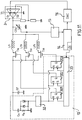
- FIG 11 The embodiment of the invention shown in Figure 11, in which components identical to those of Figure 10 are indicated by the same reference symbols or numerals, relates to an application in which the capacitive load to be driven may vary, that is, may adopt different capacitances of predetermined values.
- Various inductances are provided and can be connected in the circuit selectively in order to optimize the energy balance between the various reactive components of the resonant circuit in any situation; in this embodiment, three inductances are provided but, naturally, there may be a larger number, if necessary.
- the three inductances, indicated Lr1, Lr2 and Lr3, are connected in the resonant circuit in series with three respective electronic switches, indicated T31, T32, T33, each having its control terminal connected to the output of a respective flip-flop 301, 302 or 303 of a control unit 10' similar to the unit 10 of Figure 10.
- the capacitance value of the capacitive load at any particular time, indicated Clv in this example, is determined by the input unit 15 and is supplied to the control unit 14.
- the control unit 14 selects one of the electronic switches T31, T32, T33, more precisely, the switch which is in series with the appropriate inductance for the capacitance value Clv of the load, as well as the magnitude of the delay ⁇ t most suitable for the specific combination of capacitance and inductance and for the waveform to be produced in the capacitive load.
Landscapes
- Physics & Mathematics (AREA)
- Engineering & Computer Science (AREA)
- Microelectronics & Electronic Packaging (AREA)
- Optics & Photonics (AREA)
- Particle Formation And Scattering Control In Inkjet Printers (AREA)
- Accessory Devices And Overall Control Thereof (AREA)
- Inverter Devices (AREA)
- Amplifiers (AREA)
- Dc-Dc Converters (AREA)
Priority Applications (4)
| Application Number | Priority Date | Filing Date | Title |
|---|---|---|---|
| EP97830628A EP0920103B1 (de) | 1997-11-28 | 1997-11-28 | System zur Versorgung einer reaktiven Last |
| DE69719332T DE69719332D1 (de) | 1997-11-28 | 1997-11-28 | System zur Versorgung einer reaktiven Last |
| JP10194801A JP3062570B2 (ja) | 1997-11-28 | 1998-07-09 | リアクタンス負荷の駆動システム |
| US09/200,297 US6181031B1 (en) | 1997-11-28 | 1998-11-25 | System for driving a reactive load |
Applications Claiming Priority (1)
| Application Number | Priority Date | Filing Date | Title |
|---|---|---|---|
| EP97830628A EP0920103B1 (de) | 1997-11-28 | 1997-11-28 | System zur Versorgung einer reaktiven Last |
Publications (2)
| Publication Number | Publication Date |
|---|---|
| EP0920103A1 true EP0920103A1 (de) | 1999-06-02 |
| EP0920103B1 EP0920103B1 (de) | 2003-02-26 |
Family
ID=8230874
Family Applications (1)
| Application Number | Title | Priority Date | Filing Date |
|---|---|---|---|
| EP97830628A Expired - Lifetime EP0920103B1 (de) | 1997-11-28 | 1997-11-28 | System zur Versorgung einer reaktiven Last |
Country Status (4)
| Country | Link |
|---|---|
| US (1) | US6181031B1 (de) |
| EP (1) | EP0920103B1 (de) |
| JP (1) | JP3062570B2 (de) |
| DE (1) | DE69719332D1 (de) |
Families Citing this family (2)
| Publication number | Priority date | Publication date | Assignee | Title |
|---|---|---|---|---|
| US6538346B2 (en) * | 1998-11-25 | 2003-03-25 | Stmicroelectronics S.R.L. | System for driving a reactive load |
| CN106716835B (zh) * | 2014-09-18 | 2019-09-13 | 三美电机株式会社 | 容性负载驱动电路以及光扫描装置 |
Citations (6)
| Publication number | Priority date | Publication date | Assignee | Title |
|---|---|---|---|---|
| WO1986005304A1 (en) * | 1985-02-28 | 1986-09-12 | Motorola, Inc. | A low voltage power source power inverter for an electroluminescent device |
| GB2196805A (en) * | 1986-10-30 | 1988-05-05 | Timex Corp | Low voltage electroluminescent lamp driver circuits |
| EP0667733A1 (de) * | 1994-02-09 | 1995-08-16 | Nec Corporation | Verfahren und Gerät zum Betreiben eines Lumineszenselementes |
| US5493183A (en) * | 1994-11-14 | 1996-02-20 | Durel Corporation | Open loop brightness control for EL lamp |
| EP0730392A2 (de) * | 1995-02-28 | 1996-09-04 | Sgs-Thomson Microelectronics K.K. | Schaltung zum Betrieben einer lumineszenten Fläche |
| EP0809421A2 (de) * | 1996-05-21 | 1997-11-26 | Texas Instruments Inc. | Spannungserhöhungsreglerschaltung |
Family Cites Families (9)
| Publication number | Priority date | Publication date | Assignee | Title |
|---|---|---|---|---|
| US4691270A (en) * | 1986-07-22 | 1987-09-01 | Rca Corporation | Current fed inverter bridge with lossless snubbers |
| JPH0267006A (ja) | 1988-08-31 | 1990-03-07 | Juki Corp | 容量性負荷駆動装置 |
| US5260606A (en) * | 1992-01-31 | 1993-11-09 | Litton Systems Canada Limited | High efficiency squarewave voltage driver |
| US5264736A (en) * | 1992-04-28 | 1993-11-23 | Raytheon Company | High frequency resonant gate drive for a power MOSFET |
| KR970010485B1 (ko) * | 1994-08-25 | 1997-06-26 | 엘지전자 주식회사 | 프로젝션티브이용 램프의 다중 출력회로 |
| US5541829A (en) * | 1994-11-25 | 1996-07-30 | Matsushita Electric Works, Ltd. | Power source device |
| CN1040272C (zh) * | 1995-03-15 | 1998-10-14 | 松下电工株式会社 | 逆变装置 |
| US5559478A (en) * | 1995-07-17 | 1996-09-24 | University Of Southern California | Highly efficient, complementary, resonant pulse generation |
| JPH10174436A (ja) | 1996-12-09 | 1998-06-26 | Mitsui Chem Inc | 圧電素子駆動回路 |
-
1997
- 1997-11-28 DE DE69719332T patent/DE69719332D1/de not_active Expired - Lifetime
- 1997-11-28 EP EP97830628A patent/EP0920103B1/de not_active Expired - Lifetime
-
1998
- 1998-07-09 JP JP10194801A patent/JP3062570B2/ja not_active Expired - Fee Related
- 1998-11-25 US US09/200,297 patent/US6181031B1/en not_active Expired - Lifetime
Patent Citations (6)
| Publication number | Priority date | Publication date | Assignee | Title |
|---|---|---|---|---|
| WO1986005304A1 (en) * | 1985-02-28 | 1986-09-12 | Motorola, Inc. | A low voltage power source power inverter for an electroluminescent device |
| GB2196805A (en) * | 1986-10-30 | 1988-05-05 | Timex Corp | Low voltage electroluminescent lamp driver circuits |
| EP0667733A1 (de) * | 1994-02-09 | 1995-08-16 | Nec Corporation | Verfahren und Gerät zum Betreiben eines Lumineszenselementes |
| US5493183A (en) * | 1994-11-14 | 1996-02-20 | Durel Corporation | Open loop brightness control for EL lamp |
| EP0730392A2 (de) * | 1995-02-28 | 1996-09-04 | Sgs-Thomson Microelectronics K.K. | Schaltung zum Betrieben einer lumineszenten Fläche |
| EP0809421A2 (de) * | 1996-05-21 | 1997-11-26 | Texas Instruments Inc. | Spannungserhöhungsreglerschaltung |
Also Published As
| Publication number | Publication date |
|---|---|
| EP0920103B1 (de) | 2003-02-26 |
| DE69719332D1 (de) | 2003-04-03 |
| JPH11198373A (ja) | 1999-07-27 |
| US6181031B1 (en) | 2001-01-30 |
| JP3062570B2 (ja) | 2000-07-10 |
Similar Documents
| Publication | Publication Date | Title |
|---|---|---|
| US10075074B2 (en) | DC to DC converters and controllers thereof | |
| US7595623B2 (en) | Methods and apparatus for a spread spectrum switching regulator | |
| EP1909379B1 (de) | Verfahren und Vorrichtung zur Pulsweitenmodulation | |
| US6750637B2 (en) | Switching power supply | |
| US5905369A (en) | Variable frequency switching of synchronized interleaved switching converters | |
| CN1711670B (zh) | 用于直流/直流转换器的控制器 | |
| US6075295A (en) | Single inductor multiple output boost regulator | |
| US5814979A (en) | Low drop out switching regulator | |
| US6100677A (en) | Switching controller chip with internal but not external soft start circuitry and DC to DC converter including such a controller chip | |
| JP6702010B2 (ja) | スイッチング電源装置 | |
| US10186967B2 (en) | Switching converter with ramp-based output regulation | |
| KR101850949B1 (ko) | 용량성 부하의 구동 방법 및 그 구동 회로 | |
| US10720839B1 (en) | System and method for operating a switching converter in light load | |
| CN101911457A (zh) | 具有与占空比无关的电流限制的电源调节器系统及其调节方法 | |
| EP2166655A1 (de) | Gesteuerte Ladungspumpenanordnung und Verfahren zur Steuerung einer getakteten Ladungspumpe | |
| US9046904B2 (en) | Apparatus and method for controlling pulse frequency modulation in single-inductor dual-output power circuit | |
| US20170054272A1 (en) | Digital pulse width modulation power supply with pico second resolution | |
| US6538346B2 (en) | System for driving a reactive load | |
| WO2016144570A1 (en) | Switched mode power supply having a staircase current limit | |
| US6285174B1 (en) | Switching DC-to-Dc converter having on-time signal generation circuit and method for generating signal indicative of converter on-time | |
| US7208926B2 (en) | Switching signal modulation circuit | |
| US20040120395A1 (en) | Digital pulse modulation arrangements | |
| EP0920103B1 (de) | System zur Versorgung einer reaktiven Last | |
| US4208584A (en) | Circuit arrangement for an X-ray generator | |
| CN104426551B (zh) | 模拟数字转换器和带有在弱负载时低静电流的调节电路 |
Legal Events
| Date | Code | Title | Description |
|---|---|---|---|
| PUAI | Public reference made under article 153(3) epc to a published international application that has entered the european phase |
Free format text: ORIGINAL CODE: 0009012 |
|
| AK | Designated contracting states |
Kind code of ref document: A1 Designated state(s): DE FR GB IT |
|
| AX | Request for extension of the european patent |
Free format text: AL;LT;LV;MK;RO;SI |
|
| 17P | Request for examination filed |
Effective date: 19991124 |
|
| AKX | Designation fees paid |
Free format text: DE FR GB IT |
|
| 17Q | First examination report despatched |
Effective date: 20010924 |
|
| GRAH | Despatch of communication of intention to grant a patent |
Free format text: ORIGINAL CODE: EPIDOS IGRA |
|
| GRAH | Despatch of communication of intention to grant a patent |
Free format text: ORIGINAL CODE: EPIDOS IGRA |
|
| GRAA | (expected) grant |
Free format text: ORIGINAL CODE: 0009210 |
|
| AK | Designated contracting states |
Designated state(s): DE FR GB IT |
|
| PG25 | Lapsed in a contracting state [announced via postgrant information from national office to epo] |
Ref country code: FR Free format text: LAPSE BECAUSE OF NON-PAYMENT OF DUE FEES Effective date: 20030226 |
|
| REG | Reference to a national code |
Ref country code: GB Ref legal event code: FG4D |
|
| REF | Corresponds to: |
Ref document number: 69719332 Country of ref document: DE Date of ref document: 20030403 Kind code of ref document: P |
|
| PG25 | Lapsed in a contracting state [announced via postgrant information from national office to epo] |
Ref country code: DE Free format text: LAPSE BECAUSE OF FAILURE TO SUBMIT A TRANSLATION OF THE DESCRIPTION OR TO PAY THE FEE WITHIN THE PRESCRIBED TIME-LIMIT Effective date: 20030527 |
|
| PLBE | No opposition filed within time limit |
Free format text: ORIGINAL CODE: 0009261 |
|
| STAA | Information on the status of an ep patent application or granted ep patent |
Free format text: STATUS: NO OPPOSITION FILED WITHIN TIME LIMIT |
|
| EN | Fr: translation not filed | ||
| 26N | No opposition filed |
Effective date: 20031127 |
|
| PGFP | Annual fee paid to national office [announced via postgrant information from national office to epo] |
Ref country code: IT Payment date: 20061130 Year of fee payment: 10 |
|
| PGFP | Annual fee paid to national office [announced via postgrant information from national office to epo] |
Ref country code: GB Payment date: 20071029 Year of fee payment: 11 |
|
| GBPC | Gb: european patent ceased through non-payment of renewal fee |
Effective date: 20081128 |
|
| PG25 | Lapsed in a contracting state [announced via postgrant information from national office to epo] |
Ref country code: IT Free format text: LAPSE BECAUSE OF NON-PAYMENT OF DUE FEES Effective date: 20071128 |
|
| PG25 | Lapsed in a contracting state [announced via postgrant information from national office to epo] |
Ref country code: GB Free format text: LAPSE BECAUSE OF NON-PAYMENT OF DUE FEES Effective date: 20081128 |