EP0920124B1 - Circuit de compensation pour une amplification - Google Patents
Circuit de compensation pour une amplification Download PDFInfo
- Publication number
- EP0920124B1 EP0920124B1 EP98122467A EP98122467A EP0920124B1 EP 0920124 B1 EP0920124 B1 EP 0920124B1 EP 98122467 A EP98122467 A EP 98122467A EP 98122467 A EP98122467 A EP 98122467A EP 0920124 B1 EP0920124 B1 EP 0920124B1
- Authority
- EP
- European Patent Office
- Prior art keywords
- fet
- terminal
- resistor
- capacitor
- circuit
- Prior art date
- Legal status (The legal status is an assumption and is not a legal conclusion. Google has not performed a legal analysis and makes no representation as to the accuracy of the status listed.)
- Expired - Lifetime
Links
- 230000001447 compensatory effect Effects 0.000 title 1
- 239000003990 capacitor Substances 0.000 claims description 54
- 239000004065 semiconductor Substances 0.000 claims description 22
- 239000004020 conductor Substances 0.000 claims description 2
- 230000005669 field effect Effects 0.000 claims description 2
- 238000010586 diagram Methods 0.000 description 10
- 230000007423 decrease Effects 0.000 description 5
- 230000003287 optical effect Effects 0.000 description 5
- 101100269521 Rattus norvegicus Akap13 gene Proteins 0.000 description 2
- 230000001419 dependent effect Effects 0.000 description 2
- 230000006866 deterioration Effects 0.000 description 2
- 230000002265 prevention Effects 0.000 description 2
- 230000002194 synthesizing effect Effects 0.000 description 2
- 230000008642 heat stress Effects 0.000 description 1
- 230000003071 parasitic effect Effects 0.000 description 1
Images


Classifications
-
- H—ELECTRICITY
- H03—ELECTRONIC CIRCUITRY
- H03F—AMPLIFIERS
- H03F1/00—Details of amplifiers with only discharge tubes, only semiconductor devices or only unspecified devices as amplifying elements
- H03F1/30—Modifications of amplifiers to reduce influence of variations of temperature or supply voltage or other physical parameters
- H03F1/301—Modifications of amplifiers to reduce influence of variations of temperature or supply voltage or other physical parameters in MOSFET amplifiers
-
- H—ELECTRICITY
- H03—ELECTRONIC CIRCUITRY
- H03F—AMPLIFIERS
- H03F1/00—Details of amplifiers with only discharge tubes, only semiconductor devices or only unspecified devices as amplifying elements
- H03F1/08—Modifications of amplifiers to reduce detrimental influences of internal impedances of amplifying elements
- H03F1/22—Modifications of amplifiers to reduce detrimental influences of internal impedances of amplifying elements by use of cascode coupling, i.e. earthed cathode or emitter stage followed by earthed grid or base stage respectively
- H03F1/223—Modifications of amplifiers to reduce detrimental influences of internal impedances of amplifying elements by use of cascode coupling, i.e. earthed cathode or emitter stage followed by earthed grid or base stage respectively with MOSFET's
-
- H—ELECTRICITY
- H03—ELECTRONIC CIRCUITRY
- H03F—AMPLIFIERS
- H03F1/00—Details of amplifiers with only discharge tubes, only semiconductor devices or only unspecified devices as amplifying elements
- H03F1/56—Modifications of input or output impedances, not otherwise provided for
-
- H—ELECTRICITY
- H03—ELECTRONIC CIRCUITRY
- H03F—AMPLIFIERS
- H03F2200/00—Indexing scheme relating to amplifiers
- H03F2200/225—Indexing scheme relating to amplifiers the input circuit of an amplifying stage comprising an LC-network
-
- H—ELECTRICITY
- H03—ELECTRONIC CIRCUITRY
- H03F—AMPLIFIERS
- H03F2200/00—Indexing scheme relating to amplifiers
- H03F2200/243—A series resonance being added in series in the input circuit, e.g. base, gate, of an amplifier stage
-
- H—ELECTRICITY
- H03—ELECTRONIC CIRCUITRY
- H03F—AMPLIFIERS
- H03F2200/00—Indexing scheme relating to amplifiers
- H03F2200/447—Indexing scheme relating to amplifiers the amplifier being protected to temperature influence
-
- H—ELECTRICITY
- H03—ELECTRONIC CIRCUITRY
- H03F—AMPLIFIERS
- H03F2200/00—Indexing scheme relating to amplifiers
- H03F2200/63—Indexing scheme relating to amplifiers the amplifier being suitable for CATV applications
Definitions
- the present invention relates to a semiconductor circuit, and particularly to a semiconductor circuit used in a CATV[CAble TeleVision] hybrid IC (HIC).
- CATV[CAble TeleVision] hybrid IC HIC
- a gain slope is set by which gain of the amplifier rises with higher frequencies, but this gain slope fluctuates with variations in ambient temperature.
- Fluctuations in the gain characteristic due to variations in ambient temperature must therefore be corrected to maintain a uniform signal level over the entire CATV system.
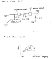
- Fig. 1 is a circuit diagram showing the configuration of a circuit disclosed in Japanese Patent Laid-open No. 83910/82 that has been used in the prior art for compensating for fluctuations in gain characteristic caused by variations in ambient temperature.
- this example of the prior art is made up of: FET(Field Effect Transistor) 125 having its gate terminal connected to input terminal 121 by way of matching circuit 126, its drain terminal connected to output terminal 122 by way of matching circuit 127, and its source terminal grounded; inductor L121 having one terminal connected to input terminal 121; resistor R121 having one terminal connected to the terminal of inductor L121 that is not connected to input terminal 121 and its other terminal connected to gate bias supply terminal 123; thermistor R122 having one terminal connected to the terminal of inductor L121 that is not connected to input terminal 121 and its other terminal grounded; and inductor L122 having one terminal connected to output terminal 122 and its other terminal connected to drain bias supply terminal 124.
- the gate bias is supplied to the gate terminal of FET 125 from gate bias supply terminal 123 by way of matching circuit 126, inductor L121, and resistor R121, and the drain bias is supplied to the drain terminal of FET 125 from drain bias supply terminal 124 by way of matching circuit 127 and inductor L122.
- the resistance of resistor R121 is set such that the relation of gate bias Vgs1 supplied from gate bias supply terminal 123 with respect to normal gate bias Vgs is: Vgs ⁇ Vgs ⁇ 1
- the gain during gate bias Vgs1 is GVgs1
- the gain during gate bias Vgs2 is GVgs2
- the gain is GVgs3 for an amplifier in which gate bias is set to Vgs in an ambient atmosphere that is at a higher temperature than room temperature
- this amplifier having a bias circuit that is not provided with thermistor R122, then: GVgs ⁇ 3 ⁇ GVgs ⁇ 2 and fluctuations in gain characteristic due to variations in ambient temperature can be compensated.
- the operating points are determined based on the DC characteristic of elements, and the high frequency characteristic is therefore dependent on the DC characteristic, and differences in the DC characteristic of elements therefore cause discrepancies in the frequency characteristic.
- Fig. 2 shows the fluctuation in the gain characteristic of the gain slope according to variations in ambient temperature.
- the bias is set by the voltage division ratio of the bleeder resistance, a plurality of elements are necessary for realizing temperature compensation, and this requirement both increases the scale of the circuit and raises costs.
- US 3,705,316 discloses a temperature-compensated light source including a thermistor, several resistors, an operational amplifier, and a light-emitting diode combined in such a manner that the non-linear characteristics of the thermistor cause the operational amplifier to vary the energizing current supplied to the LED to compensate for the non-linear temperature characteristics of the diode.
- US 5,347,389 discloses an optical receiver for an optical signal amplitude modulated with broadband RF sigals. It includes an optical detector which receives the optical signal and generates a radio frequency electrical signal which varies with the intensity level of the incoming optical signal.
- US 4,352,053 discloses a temperature compensating voltage generator circuit for compensating temperature characteristics of an electric circuit whose electrical characteristic varies in accordance with the change of the ambient temperature and whose electrical characteristic can be changed or controlled by a control voltage.
- the temperature compensating voltage generator circuit comprising a plurality of temperature-sensitive resistor circuits, a plurality of diode circuits and one or more resistor circuits.
- WO 97/05695 discloses an amplifier circuit for a cable access television line amplifier including a first cascode amplifier and a second cascode amplifier covered in a push-pull arrangement.
- a first and second transimpedance amplifier includes a FET as an active load so as to provide feedback.
- the object of the present invention is to provide a semiconductor circuit that can compensate for fluctuations in the gain characteristic of the gain slope in the event of variations in ambient temperature without increasing the scale of the circuit or raising costs.
- a thermistor which is a thermally sensitive resistance element having a negative temperature characteristic according to the ambient temperature
- the Q value which is the factor indicating the resonance point level
- the Q value decreases to the degree that the resistance of the thermistor rises, the Q value thus becoming large as the ambient temperature rises and becoming small as the ambient temperature falls.
- the inclination of the gain slope in a semiconductor element becomes gentle, but when the ambient temperature falls, the gain increases and the inclination of the gain slope becomes steep. Fluctuation in the value Q with respect to the ambient temperature is therefore canceled by fluctuation in gain characteristic of the gain slope with respect to the ambient temperature, whereby the inclination characteristic of the gain slope is uniform even in the event of changes in the ambient temperature.
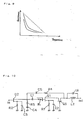
- Fig. 3 is a circuit diagram showing the configuration of a semiconductor circuit according to the first embodiment of the present invention, and principally shows the circuit that compensates for fluctuations in gain characteristic of the gain slope with respect to ambient temperature. This circuit is only the alternating-current portion of the semiconductor circuit of this invention.
- this embodiment is made up of first FET Q1, the drain side of which is the output terminal; first inductor L1 having one terminal connected to the gate terminal of FET Q1; thermistor Rt which is the first resistance that is a thermally sensitive resistance element having resistance that changes with a negative temperature characteristic according to the ambient temperature and having one terminal connected to the terminal of inductor L1 that is not connected to FET Q1; first capacitor C1 connected between the terminal of thermistor Rt that is not connected to inductor L1 and the input terminal; and third resistance R1 and second capacitor C2 that are connected in parallel between the source terminal of FET Q1 and ground.
- Resistance R1 and second capacitor C2 are elements that regulate frequency characteristics and are not essential components of the present invention.
- Thermistor Rt which is provided as the input resistance of FET Q1, has a negative temperature characteristic and therefore has low resistance when the ambient temperature is high and high resistance when the ambient temperature is low.
- Fig. 4 shows one example of the gain characteristic with respect to frequency in a typical resonant circuit.
- Fig. 5 is provided to illustrate the gain characteristic with respect to frequency in the circuit shown in Fig. 3.
- the value of Q decreases to the extent that the resistance of thermistor Rt increases and increases to the extent that the resistance of thermistor Rt decreases as shown in the above equations, and as shown in Fig. 5, the value of Q thus increases when the ambient temperature rises and decreases when the ambient temperature falls.
- the circuit shown in Fig. 3 can achieve frequency-gain characteristics due to variations in ambient temperature such as shown in Fig. 5, but in a circuit that realizes a gain slope, increase in the ambient temperature results in a gentle inclination of the gain slope, and decrease in the ambient temperature results in increased gain and a steep inclination of the gain slope.
- Fig. 6 shows the inclination characteristic of the gain slope with respect to ambient temperature when using the circuit shown in Fig. 3.
- the inclination characteristic of the gain slope in this embodiment does not change despite variations in ambient temperature.
- inductor L1 can be constituted by the bonding wire or conductor pattern that connects the gate terminal of FET Q1 and thermistor Rt.
- Fig. 7 presents a detailed view of the gate input portion of FET Q1 shown in Fig. 3.
- Fig. 8 is a circuit diagram showing the configuration of the semiconductor circuit according to the third embodiment of the present invention. This circuit is only the alternating-current portion of the semiconductor circuit of this invention.
- this embodiment is of a configuration in which second resistance R5 in parallel with thermistor Rt is added to the circuit shown in Fig. 3.
- Fig. 9 shows an example of the characteristics of thermistors having a negative temperature characteristic.
- thermistors on the market do not provide a continuum of characteristics, each having their own predetermined characteristics.
- the desired characteristic can be obtained by connecting resistance R5 having any resistance in parallel with thermistor Rt as shown in Fig. 8.
- Fig. 10 is a circuit diagram showing the semiconductor circuit according to the fourth embodiment of the present invention. This figure shows the circuit shown in Fig. 3 in more concrete terms. This circuit is only the alternating-current portion of the semiconductor circuit of this invention.
- this embodiment is provided on the input side of the circuit shown in Fig. 3 with: second FET Q2 that takes as the input terminal the gate side between input terminal and capacitor C1 and that has its drain terminal connected to capacitor C1, fourth resistor R2 and third capacitor C3 connected in parallel between the source terminal of FET Q2 and ground, and fifth resistance R3 and fourth capacitor C4 connected in series between the drain terminal of FET Q2 and ground; and is provided on the output side of the circuit shown in Fig.
- third FET Q3 having its source terminal connected to the drain terminal of FET Q1, its gate terminal connected to ground; sixth resistance R4 and fifth capacitor C5 connected in series between the drain terminal of FET Q3 and the drain terminal of FET Q2 and provided as a feedback loop; and, functioning as a resonant circuit, sixth capacitor C6 and second inductor L2 connected in parallel between the output terminal and the drain terminal of FET Q3.
- a gain slope with gentle inclination is generated when the ambient temperature rises and a gain slope with steep inclination is generated when the ambient temperature drops in the resonant circuit made up of capacitor C6 and inductor L2.
- fluctuation of the value of Q in the circuit shown in Fig. 3 with respect to the ambient temperature is canceled by the fluctuation in the gain characteristic with respect to ambient temperature of the gain slop generated in the resonant circuit made up of capacitor C6 and inductor L2, and the inclination characteristic of the gain slope is thus fixed regardless of variations in the ambient temperature.
- Fig. 11 is a circuit diagram showing the semiconductor circuit according to the fifth embodiment of the present invention.
- inputted signals in this embodiment are distributed into two different signals, the two distributed signals each being amplified by amplifier circuits 12 and 13, and the signals amplified in amplifier circuits 12 and 13 then being synthesized and outputted.
- Transformer T1 which is grounded by way of capacitors C34 and C35, is provided as a distributing means for distributing signals inputted by way of input terminal 1 into two signals of different phase; and transformer T2, which is grounded by way of capacitor C37, is provided as a synthesizing means for synthesizing the two signals amplified by amplifier circuits 12 and 13 as one signal.
- Amplifier circuit 12 is made up of: FETs Q11-Q13 connected in multiple stages; thermistor Rt11 and resistor R13 connected in parallel and provided as the gate resistance of FET Q11, which is the second stage; inductor L13 provided between the gate terminal of FET Q11 and the connection point between thermistor Rt11 and resistor R13; resistor R11, capacitor C11, and thermistor Rt12 connected in a series between the drain terminal and gate terminal of FET Q12, the gate terminal being the input of amplifier circuit 12; resistor R12 and capacitor C12 connected in a series between the drain terminal of FET Q12 and a prescribed potential; capacitor C13 connected between the connection point between thermistor Rt11 and resistor R13 and the drain terminal of FET Q12; inductor L11 and resistor R17 connected in a series between the drain terminal of FET Q12 and the source terminal of FET Q11; capacitor C15 connected between the connection point of inductor L11 and resistor R17 and a prescribed potential;
- Amplifier circuit 13 is made up of: FETs Q21-Q23 connected in multiple stages; thermistor Rt21 and resistor R23 connected in parallel and provided as the gate resistance of FET Q21, which is the second stage; inductor L23 provided between the gate terminal of FET Q21 and the connection point between thermistor Rt21 and resistor R23; resistor R21, capacitor C21, and thermistor Rt22 connected in a series between the drain terminal and gate terminal of FET Q22, the gate being the input of amplifier circuit 13; resistor R22 and capacitor C22 connected in a series between the drain terminal of FET Q22 and a prescribed potential; capacitor C23 connected between the connection point between thermistor Rt21 and resistor R23 and the drain terminal of FET Q22; inductor L21 and resistor R27 connected in a series between the drain terminal of FET Q22 and the source terminal of FET Q21; capacitor C25 connected between the connection point of inductor L21 and resistor R27 and a prescribed potential; resist
- gate terminal of FET Q13 and the gate terminal of FET Q23 are connected together by way of resistors R16 and R26.
- the input side of transformer T1 is provided with: capacitor C33 and inductor L31 connected in a series between transformer T1 and input terminal 1; capacitor C31 and resistor R31 connected in a series between the connection point of capacitor C33 and inductor L31 and a prescribed potential; and capacitor C32 connected between the connection point between capacitor C33 and inductor L31 and a prescribed potential; and the output side of transformer T2 is provided with: inductor L32 and capacitor C39 connected in a series between transformer T2 and output terminal 2; and capacitor C38 connected between the connection point between inductor L32 and capacitor C39 and a prescribed potential.
- resistor R41 between the source terminal of FET Q11 and the source terminal of FET Q21; resistors R39 and R40 connected in a series between the gate terminal of FET Q11 and the gate terminal of FET Q21; resistors R33 and R34 connected in a series between the connection point between resistor R39 and resistor R40 and transformer T1; resistor R32 and thermistors Rt31 and Rt32 connected in a series between the connection point between resistor R33 and transformer T1 and a prescribed potential; resistor R35 connected between a prescribed potential and the connection point between resistor R34 and the connection point between resistors R39 and R40; resistor R37 connected between the source terminal of FET Q12 and the source terminal of FET Q22; resistor R36 connected between the source terminal of FET Q12 and a prescribed potential; resistor R38 connected between the source terminal of FET Q22 and a prescribed potential; resistors R42 and R43 connected between the connection point between resistor R16 and resist
- Thermistors Rt11, Rt21, and Rt31 are thermally sensitive resistance elements in which resistance changes with a negative temperature characteristic according to the ambient temperature
- thermistors Rt12, Rt13, Rt22, Rt23 and Rt32 are thermally sensitive resistance elements in which resistance changes with a positive temperature characteristic according to the ambient temperature.
- the circuit shown in Fig. 3 that is made up of capacitor C1, thermistor Rt, inductor L1 and FET Q1 is constituted by capacitor C13, thermistor Rt11, inductor L13 and FET Q11 in amplifier circuit 12, and this circuit functions such that fluctuations in the gain characteristic with respect to ambient temperature of the gain slope of the resonant circuit made up by inductor L12 and capacitor C16 in amplifier circuit 12 are canceled by fluctuations of the value of Q with respect to ambient temperature in the circuit made up of capacitor C13, thermistor Rt11, and inductor L13.
- the inclination characteristic of the gain slope outputted from amplifier circuit 12 is fixed despite variations in ambient temperature.
- the circuit shown in Fig. 3 that is made up by capacitor C1, thermistor Rt, inductor L1 and FET Q1 is constituted by capacitor C23, thermistor Rt21, inductor L23, and FET Q21; and this circuit functions such that fluctuations in the gain characteristic with respect to ambient temperature in the gain slope generated by the resonant circuit made up by inductor L22 and capacitor C26 in amplifier circuit 13 are canceled by fluctuations in the value of Q with respect to ambient temperature in the circuit made up by capacitor C23, thermistor Rt21, and inductor L23, whereby the inclination characteristic of the gain slope outputted from amplifier circuit 13 is uniform despite variations in ambient temperature.
- inductor L12 and capacitor C16 as well as inductor L22 and capacitor C26 that constitute the resonant circuits that generate the gain slope are each provided outside the feedback loops.
- thermistors Rt31 and Rt32 are connected in a series between the connection point between resistor R33 and transformer T1 and a prescribed potential.
- the current is a minimum value in the vicinity of a prescribed temperature, and the circuit current increases as the ambient temperature falls from a prescribed temperature or as the ambient temperature rises from a prescribed temperature, thereby enabling prevention of deterioration of distortion characteristic due to changes in temperature.
- resistor R43 having a resistance of 10-100 ⁇ is provided between resistor R42 and the connection point between resistor R16 and resistor R26, and capacitor C40 is provided between the connection point between resistor R42 and resistor R43 and a prescribed potential, the circuit constants of these components being set according to termination conditions.
Landscapes
- Engineering & Computer Science (AREA)
- Power Engineering (AREA)
- Amplifiers (AREA)
Claims (6)
- Circuit à semi-conducteurs comportant :un premier Transistor à Effet de champ (FET) (Q1), etune première inductance (L1), une première résistance (Rt), et un premier condensateur (C1) reliés en série entre une borne d'entrée et une borne de grille dudit premier transistor FET,dans lequel ladite première résistance (Rt) est un élément thermiquement sensible qui change de résistance en fonction de la température ambiante et a une caractéristique de température négative, et ladite borne d'entrée recevant des signaux d'entrée externes, qui sont amplifiés dans ledit premier transistor FET.
- Circuit à semi-conducteurs selon la revendication 1, dans lequel ladite première inductance (L1) est formée à partir d'un motif de film ou conducteur de connexion.
- Circuit à semi-conducteurs selon la revendication 1, comportant une deuxième résistance (R5) qui est reliée en parallèle à ladite première résistance.
- Circuit à semi-conducteurs selon la revendication 2, comportant une deuxième résistance (R5) reliée en parallèle à ladite première résistance.
- Circuit à semi-conducteurs selon l'une des revendications 1 à 4, comportant :une troisième résistance (R1) et un deuxième condensateur (C2) reliés en parallèle entre une borne de source dudit premier transistor FET et la terre,un deuxième transistor FET (Q2) fourni entre ledit premier condensateur et ladite borne d'entrée et ayant sa borne de drain reliée audit premier condensateur (C1) et sa borne de grille reliée à ladite borne d'entrée,une quatrième résistance (R2) et un troisième condensateur (C3) reliés en parallèle entre une borne de source dudit deuxième transistor FET et la terre,une cinquième résistance (R3) et un quatrième condensateur (C4) reliés en série entre une borne de drain dudit deuxième transistor FET et la terre,un troisième transistor FET (Q3) fourni entre ledit premier transistor FET et une borne de sortie du côté du drain dudit premier transistor FET et ayant sa borne de grille reliée à la terre, sa borne de source reliée à la borne de drain dudit premier transistor FET (Q1), et sa borne de drain reliée à ladite borne de sortie,une sixième résistance (R4) et un cinquième condensateur (C5) reliés en série entre une borne de drain dudit troisième transistor FET et la borne de drain dudit deuxième transistor FET, etun circuit résonant (L2 ; C6) entre la borne de drain dudit troisième transistor FET et ladite borne de sortie.
- Circuit à semi-conducteurs selon la revendication 5, dans lequel ledit circuit résonant est constitué d'une seconde inductance (L2) et d'un sixième condensateur (C6) en connexion parallèle.
Applications Claiming Priority (3)
| Application Number | Priority Date | Filing Date | Title |
|---|---|---|---|
| JP32644597 | 1997-11-27 | ||
| JP32644597 | 1997-11-27 | ||
| JP326445/97 | 1997-11-27 |
Publications (3)
| Publication Number | Publication Date |
|---|---|
| EP0920124A2 EP0920124A2 (fr) | 1999-06-02 |
| EP0920124A3 EP0920124A3 (fr) | 2001-10-24 |
| EP0920124B1 true EP0920124B1 (fr) | 2007-03-07 |
Family
ID=18187895
Family Applications (1)
| Application Number | Title | Priority Date | Filing Date |
|---|---|---|---|
| EP98122467A Expired - Lifetime EP0920124B1 (fr) | 1997-11-27 | 1998-11-26 | Circuit de compensation pour une amplification |
Country Status (5)
| Country | Link |
|---|---|
| US (1) | US6147557A (fr) |
| EP (1) | EP0920124B1 (fr) |
| KR (1) | KR100339295B1 (fr) |
| CN (1) | CN1088940C (fr) |
| DE (1) | DE69837246T2 (fr) |
Families Citing this family (4)
| Publication number | Priority date | Publication date | Assignee | Title |
|---|---|---|---|---|
| US6657425B2 (en) * | 2001-06-26 | 2003-12-02 | Koninklijke Philips Electronics N.V. | Power measurement circuit including harmonic filter |
| JP2006129443A (ja) * | 2004-09-30 | 2006-05-18 | Renesas Technology Corp | 高周波電力増幅器 |
| WO2020006185A1 (fr) | 2018-06-27 | 2020-01-02 | Viasat, Inc. | Amplificateur à égaliseur de pente de gain intégré |
| US10931274B2 (en) * | 2019-01-18 | 2021-02-23 | Globalfoundries U.S. Inc. | Temperature-sensitive bias circuit |
Family Cites Families (15)
| Publication number | Priority date | Publication date | Assignee | Title |
|---|---|---|---|---|
| US3566288A (en) * | 1968-11-29 | 1971-02-23 | Avco Corp | Vhf solid state amplifier |
| US3705316A (en) * | 1971-12-27 | 1972-12-05 | Nasa | Temperature compensated light source using a light emitting diode |
| US4011518A (en) * | 1975-10-28 | 1977-03-08 | The United States Of America As Represented By The Secretary Of The Navy | Microwave GaAs FET amplifier circuit |
| US4207538A (en) * | 1978-08-29 | 1980-06-10 | Rca Corporation | Temperature compensation circuit |
| EP0039215B1 (fr) * | 1980-04-28 | 1985-08-07 | Fujitsu Limited | Circuit générateur d'une tension de compensation en température |
| JPS5783910A (en) * | 1980-11-13 | 1982-05-26 | Fujitsu Ltd | Microwave amplifier |
| JPS57157606A (en) * | 1981-03-24 | 1982-09-29 | Nec Corp | Fet amplifier |
| JPS6297411A (ja) * | 1985-10-23 | 1987-05-06 | Nec Corp | Fet増幅器の温度補償回路 |
| JPH02280511A (ja) * | 1989-04-21 | 1990-11-16 | Matsushita Electric Ind Co Ltd | Fet増幅器 |
| US4967169A (en) * | 1989-07-31 | 1990-10-30 | Teledyne Mec | FET monolithic microwave integrated circuit variable slope gain-equalizer |
| JPH03283458A (ja) * | 1990-03-30 | 1991-12-13 | Hitachi Ltd | Icの温度補償回路 |
| US5157352A (en) * | 1991-11-04 | 1992-10-20 | Electronic Instrumentation And Technology Inc. | Bias current control for operational amplifier current/voltage converters |
| US5347389A (en) * | 1993-05-27 | 1994-09-13 | Scientific-Atlanta, Inc. | Push-pull optical receiver with cascode amplifiers |
| US5408697A (en) * | 1993-06-14 | 1995-04-18 | Qualcomm Incorporated | Temperature-compensated gain-controlled amplifier having a wide linear dynamic range |
| US5742205A (en) * | 1995-07-27 | 1998-04-21 | Scientific-Atlanta, Inc. | Field effect transistor cable television line amplifier |
-
1998
- 1998-11-19 US US09/195,621 patent/US6147557A/en not_active Expired - Lifetime
- 1998-11-26 KR KR1019980051010A patent/KR100339295B1/ko not_active Expired - Fee Related
- 1998-11-26 DE DE69837246T patent/DE69837246T2/de not_active Expired - Fee Related
- 1998-11-26 EP EP98122467A patent/EP0920124B1/fr not_active Expired - Lifetime
- 1998-11-27 CN CN98124877A patent/CN1088940C/zh not_active Expired - Fee Related
Also Published As
| Publication number | Publication date |
|---|---|
| EP0920124A2 (fr) | 1999-06-02 |
| DE69837246D1 (de) | 2007-04-19 |
| EP0920124A3 (fr) | 2001-10-24 |
| CN1088940C (zh) | 2002-08-07 |
| KR19990045612A (ko) | 1999-06-25 |
| DE69837246T2 (de) | 2007-11-08 |
| CN1219022A (zh) | 1999-06-09 |
| US6147557A (en) | 2000-11-14 |
| KR100339295B1 (ko) | 2002-07-18 |
Similar Documents
| Publication | Publication Date | Title |
|---|---|---|
| US6476679B2 (en) | Semiconductor circuit with a stabilized gain slope | |
| US5406224A (en) | Circuit for stabilizing RF amplifier | |
| US20020125945A1 (en) | Method and apparatus for protecting radio frequency power amplifiers | |
| EP0920125B1 (fr) | Amplificateur à semi-conducteur de type "push-pull" à large bande | |
| KR100330954B1 (ko) | 주변온도변화에의해발생된왜곡을보상하는반도체회로 | |
| US4617522A (en) | Temperature regulated feedforward amplifier | |
| JP3381283B2 (ja) | 可変リアクタンス回路およびこれを用いた可変整合回路 | |
| US5367268A (en) | Transmission signal output control circuit | |
| US5939920A (en) | Method and apparatus which adds distortion to a signal to compensate for distortion added at a later stage by a nonlinear element | |
| EP0920124B1 (fr) | Circuit de compensation pour une amplification | |
| JP3150112B2 (ja) | 半導体回路 | |
| EP1054508B1 (fr) | Amplificateur de micro-ondes | |
| US4540956A (en) | High frequency band-pass amplifier with adjustable impedance and oscillator including it | |
| KR100895961B1 (ko) | 제어 가능한 조정 소자 및 안테나 증폭기 | |
| JP3150111B2 (ja) | 半導体回路 | |
| JPH03258008A (ja) | 位相温度補償型高周波増幅器 | |
| JPH11220336A (ja) | 半導体回路 | |
| JPH10215123A (ja) | 電力増幅器 | |
| KR100315470B1 (ko) | 하이브리드증폭기에서온도변화에의한입출력임피던스보상회로 | |
| JPH11220339A (ja) | 半導体回路 | |
| JPH1032442A (ja) | 温度補償機能付き可変減衰器 | |
| JPH02135811A (ja) | 同調回路 |
Legal Events
| Date | Code | Title | Description |
|---|---|---|---|
| PUAI | Public reference made under article 153(3) epc to a published international application that has entered the european phase |
Free format text: ORIGINAL CODE: 0009012 |
|
| AK | Designated contracting states |
Kind code of ref document: A2 Designated state(s): AT BE CH CY DE DK ES FI FR GB GR IE IT LI LU MC NL PT SE Kind code of ref document: A2 Designated state(s): DE FR GB |
|
| AX | Request for extension of the european patent |
Free format text: AL;LT;LV;MK;RO;SI |
|
| PUAL | Search report despatched |
Free format text: ORIGINAL CODE: 0009013 |
|
| AK | Designated contracting states |
Kind code of ref document: A3 Designated state(s): AT BE CH CY DE DK ES FI FR GB GR IE IT LI LU MC NL PT SE |
|
| AX | Request for extension of the european patent |
Free format text: AL;LT;LV;MK;RO;SI |
|
| RIC1 | Information provided on ipc code assigned before grant |
Free format text: 7H 03F 1/30 A, 7H 03F 1/56 B |
|
| 17P | Request for examination filed |
Effective date: 20020213 |
|
| 17Q | First examination report despatched |
Effective date: 20020528 |
|
| AKX | Designation fees paid |
Free format text: DE FR GB |
|
| RAP1 | Party data changed (applicant data changed or rights of an application transferred) |
Owner name: NEC COMPOUND SEMICONDUCTOR DEVICES, LTD. |
|
| RAP1 | Party data changed (applicant data changed or rights of an application transferred) |
Owner name: NEC ELECTRONICS CORPORATION |
|
| GRAP | Despatch of communication of intention to grant a patent |
Free format text: ORIGINAL CODE: EPIDOSNIGR1 |
|
| GRAS | Grant fee paid |
Free format text: ORIGINAL CODE: EPIDOSNIGR3 |
|
| GRAA | (expected) grant |
Free format text: ORIGINAL CODE: 0009210 |
|
| AK | Designated contracting states |
Kind code of ref document: B1 Designated state(s): DE FR GB |
|
| REG | Reference to a national code |
Ref country code: GB Ref legal event code: FG4D |
|
| REF | Corresponds to: |
Ref document number: 69837246 Country of ref document: DE Date of ref document: 20070419 Kind code of ref document: P |
|
| ET | Fr: translation filed | ||
| PLBE | No opposition filed within time limit |
Free format text: ORIGINAL CODE: 0009261 |
|
| STAA | Information on the status of an ep patent application or granted ep patent |
Free format text: STATUS: NO OPPOSITION FILED WITHIN TIME LIMIT |
|
| 26N | No opposition filed |
Effective date: 20071210 |
|
| PGFP | Annual fee paid to national office [announced via postgrant information from national office to epo] |
Ref country code: DE Payment date: 20081120 Year of fee payment: 11 |
|
| PGFP | Annual fee paid to national office [announced via postgrant information from national office to epo] |
Ref country code: FR Payment date: 20081112 Year of fee payment: 11 |
|
| PGFP | Annual fee paid to national office [announced via postgrant information from national office to epo] |
Ref country code: GB Payment date: 20081126 Year of fee payment: 11 |
|
| GBPC | Gb: european patent ceased through non-payment of renewal fee |
Effective date: 20091126 |
|
| REG | Reference to a national code |
Ref country code: FR Ref legal event code: ST Effective date: 20100730 |
|
| PG25 | Lapsed in a contracting state [announced via postgrant information from national office to epo] |
Ref country code: FR Free format text: LAPSE BECAUSE OF NON-PAYMENT OF DUE FEES Effective date: 20091130 |
|
| PG25 | Lapsed in a contracting state [announced via postgrant information from national office to epo] |
Ref country code: DE Free format text: LAPSE BECAUSE OF NON-PAYMENT OF DUE FEES Effective date: 20100601 |
|
| PG25 | Lapsed in a contracting state [announced via postgrant information from national office to epo] |
Ref country code: GB Free format text: LAPSE BECAUSE OF NON-PAYMENT OF DUE FEES Effective date: 20091126 |