EP0920671B1 - Deformation eines digitalen bildes mit effizienter berechnung - Google Patents
Deformation eines digitalen bildes mit effizienter berechnung Download PDFInfo
- Publication number
- EP0920671B1 EP0920671B1 EP97920043A EP97920043A EP0920671B1 EP 0920671 B1 EP0920671 B1 EP 0920671B1 EP 97920043 A EP97920043 A EP 97920043A EP 97920043 A EP97920043 A EP 97920043A EP 0920671 B1 EP0920671 B1 EP 0920671B1
- Authority
- EP
- European Patent Office
- Prior art keywords
- image signal
- upsampled
- warped
- produce
- samples
- Prior art date
- Legal status (The legal status is an assumption and is not a legal conclusion. Google has not performed a legal analysis and makes no representation as to the accuracy of the status listed.)
- Expired - Lifetime
Links
Images
Classifications
-
- G—PHYSICS
- G06—COMPUTING OR CALCULATING; COUNTING
- G06T—IMAGE DATA PROCESSING OR GENERATION, IN GENERAL
- G06T3/00—Geometric image transformations in the plane of the image
- G06T3/40—Scaling of whole images or parts thereof, e.g. expanding or contracting
- G06T3/4007—Scaling of whole images or parts thereof, e.g. expanding or contracting based on interpolation, e.g. bilinear interpolation
-
- G—PHYSICS
- G06—COMPUTING OR CALCULATING; COUNTING
- G06T—IMAGE DATA PROCESSING OR GENERATION, IN GENERAL
- G06T3/00—Geometric image transformations in the plane of the image
- G06T3/40—Scaling of whole images or parts thereof, e.g. expanding or contracting
- G06T3/4084—Scaling of whole images or parts thereof, e.g. expanding or contracting in the transform domain, e.g. fast Fourier transform [FFT] domain scaling
Definitions
- This invention relates to a method and apparatus of digitally processing image data and, particularly, a method and apparatus for performing a high quality digital image warp.
- Wolberg George: "Digital Image Warping” 1992, IEEE Computer Society Press, Los Alamitos, California, USA describes digital image warping. According to Wolberg image warping is a geometric transformation. The geometric transformation of digital images is inherently a sampling process. As with all sampled data, digital images are susceptible to aliasing artefacts. Aliasing can be reduced by point sampling at a higher resolution. This raises the nyquist limit, accounting for signals with higher bandwidths. Generally, though, the display resolution places a limit on the highest frequency that can be displayed and thus limits the nyquist rate to one cycle every two pixels.
- the basic flaw in point sampling is that a discrete pixel actually represents an area, not a point. In this manner each output pixel should be considered a window looking onto the input image. Rather than sampling a point, we must instead apply a low-pass filter (LPF) upon the projected area in order to properly reflect the information content being mapped onto the output pixel.
- LPF low-pass filter
- This approach is called area sampling and the projected area is known as the pre-image.
- the low-pass filter comprises the pre-filtering stage. It serves to defeat aliasing by bandlimiting the input image prior to re-sampling onto the output grid.
- each output pixel value is evaluated by computing a weighted average of the samples taken from their respective pre-images. For example if the super-sampling grid is three times denser than the output grid (i.e. there are nine grid points per pixel area), each output pixel will be an average of the nine samples taken from its projection in the input image.
- Super-sampling reduces aliasing by band limiting the input signal.
- the purpose of the high resolution super-sampling grid is to refine the estimate of the pre-images seen by the output pixels.
- the samples then enter the pre-filtering stage consisting of a low-pass filter. This permits the input to be re-sampled onto the relatively low resolution output grid without any offending high frequencies introducing aliasing artefacts.
- an output pixel is sub-divided into nine sub-pixel samples which each undergo inverse mapping, sampling the input at nine positions. These nine values then pass through a low-pass filter to be averaged into a single output value.
- US-A-5,355,328 discloses a system for resizing a digital image.
- the digital image samples are provided to an upsampler which upsamples the samples by a factor L.
- the upsampled samples are provided to a composite filter and then downsampled by a factor M. If the input samples have a sampling period P then the output samples have a period (M/L)P which is less than P.
- a spatial transformation defines a geometric relationship between each point in an input and a warped image.
- Inverse mapping maps a pixel value in the warped image to a pixel value in the input image which may be located between pixels in the input image. Therefore, it is desirable to use interpolation to generate the pixel value from the non-integral positions in the input image.
- Bilinear interpolation uses a local. neighbourhood of four pixels and a weighted average of those four pixels for the interpolation. For a real-time implementation four pixel values are accessed simultaneously every clock cycle. The four pixel values are then multiplied by the appropriate weights and summed to produce a pixel value in the warped image.
- the next higher quality interpolator uses a three-by-three pixel area in the input image to compute each pixel value in the warped image.
- the complexity and expense of this type warper dramatically increases relative to that of a bilinear interpolator.
- Nine separate memories, nine coefficients, and a nine term sum of products is required. In applications where size, power, and cost are at a premium, this is an unacceptable solution. If a better interpolation is required, for example, four-by-four or greater, this problem is compounded.
- an image processing system comprising: means for applying an input image signal to the image processing system; upsampling means for upsampling the input image signal to produce input image signal samples uniformly sampled at a sample rate greater than the Nyquist rate by a predetermined factor greater than or equal to two, to produce an unsampled image signal; and means for warping the unsampled image signal and for down sampling the upsampled warped image signal by the said factor to produce a warped image output signal.
- An embodiment of the present invention is directed to a digital image warper system which produces a warped image from an input image.
- the warper system increases the sampling rate of a sampled image above the Nyquist rate or samples an analogue image at a higher rate than the Nyquist rate.
- the upsampled image is warped using an interpolator for resampling to produce a warped upsampled image.
- the interpolator is, for example, a low quality interpolator such as a bilinear interpolator.
- the warper image is down sampled to the same resolution as the input image to produce the warped image. Down sampling and warping can be combined into one step by modifying the geometric transformation function implemented when warping the upsampled image.
- the exemplary embodiment of the present invention is directed to a digital image warper system which produces a warped image from an input image.
- the warper system increases the sampling rate of a sampled image above the Nyquist rate.
- digital images to be warped are sampled at the Nyquist rate.
- Increasing the sampling rate reduces the spatial frequencies represented by a fixed number of samples.
- the increased sampling rate is accomplished by sampling the analog image at a higher rate than the Nyquist rate or by digitally processing an already Nyquist sampled image to increase its sampling rate (e.g. by doubling or tripling each sample).
- the later of these two approaches maintains the modularity of the warper system within a larger image processing system.
- the upsampled image is warped, using an interpolator for resampling, to produce a warped upsampled image.
- the interpolator can be a relatively low quality interpolator such as a bilinear interpolator.
- the warped image is then down sampled to the same resolution as the input image to produce the warped image. Down sampling and warping can be combined into one component by modifying the geometric transformation function implemented when warping the upsampled image.
- Fig. 1 illustrates the digital image warping system 5 according to an exemplary embodiment of the present invention.
- An input image signal 205 is provided to upsampler 10.
- the input image signal 205 is sampled at or above the Nyquist rate and is a complete representation of the underlying analog image.
- Upsampler 10 interpolates the input image signal 205 by a factor of, for example, 2 N , where N is a positive integer greater than zero, to increase the number of samples, i.e. pixel values, in the input image signal 205. Interpolation is not limited to a factor of 2 N .
- Upsampling is performed in the vertical and horizontal directions of the input image signal 205 using the same sample multiplication factor. For example, if the input image 205 has 512 pixel values by 512 pixel values, upsampling by a factor of two produces an upsampled image signal 207 having 1024 pixel values by 1024 pixel values. Upsampling by a factor of four produces an upsampled image signal 207 having a size of 2048 pixel values by 2048 pixel values. The input image signal 205 is, for example, 256 pixel values by 256 pixel values. Thus, upsampling by a factor of two produces an upsampled image signal 207 having 512 pixel values by 512 pixel values.
- upsampler 10 can be provided with an analog input signal.
- upsampler 10 samples the analog input signal at a rate of 2 N times the Nyquist rate to produce the upsampled image signal 207, where N is positive integer.
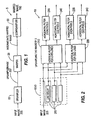
- Upsampler 10 is a high quality interpolation filter shown in Figure 2. Upsampler 10 upsamples the input image signal 205 by a factor of two in both directions using a separable filter. Upsampler 10 slightly peaks the frequency components that will be attenuated by warper 20, shown in Figure 1, to improve the image quality of the warped image.
- the input image signal 205 is provided to vertical filter 210 and vertical filter 220 directly and via line delays 200 each of which delays an entire line of the input image for one line period.
- Vertical filter 210 is a unity filter and passes the pixel values of the even lines of the input image signal 205.
- Vertical filter 220 is a four tap filter with the coefficient values selected to be a sum of the powers of 2.
- the coefficient values are -.09375, .59375, .59375, and -.09375 which are respectively -3/32, 19/32, 19/32, and -3/32.
- the multiplication operations used to implement vertical filter 220 are simplified to arithmetic shift and sum operations by using these coefficient values.
- the pixel values from vertical filters 210 and 220 are provided to (1) horizontal filters 230 which are unity filters and pass the even pixel values and (2) horizontal filters 240 which are four tap filters.
- the coefficient values of horizontal filters 240 are selected to be a sum of the powers of 2 and are -.09375, .59375, .59375, and -.09375.
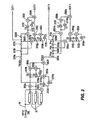
- FIG 3 is a more detailed block diagram of upsampler 10 shown in figure 2.
- Pixel values from a line of the input image signal 205 are provided to input terminal IN.
- the lines of the input image signal 205 are processed through line delays 200, adders 300a-300f, and multipliers 310a-310e to vertically interpolate the odd lines of the input image and produce vertically interpolated lines Vodd which become the odd numbered lines of the upsampled image 207, shown in Fig. 1.
- Coefficients C0, C1, and C2 are 1/16, 1/32, and 1/2, respectively.
- the output signal Veven of the upsampler 10 are not vertically filtered. These lines become the even numbered lines of the upsampled image 207 and represent the image samples of the input image as they were received.
- the even lines Veven are provided to and processed using pixel delays 320a-320d, adders 300h-3001, and multipliers 310f-310i to horizontally interpolate the pixels in the even lines Veven to produce output pixel signal OUT2 which represents the odd pixels in the even lines of the upsampled image 207, shown in Fig. 1.
- the even pixels in the output image signal are not horizontally interpolated and are provided as output pixel signal OUT1.
- the vertically interpolated lines Vodd are provided to and processed using pixel delays 320e-320g, adders 300m-300r, and multipliers 310j-310n to produce horizontally interpolated odd pixels in the vertically interpolated lines Vodd to produce output pixel signal OUT4.
- the pixels of the vertically interpolated lines Vodd are also provided, without further interpolation, as pixel signal OUT3.
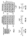
- Figure 4 illustrates the conceptual operation of upsampler 10 shown in Figures 2 and 3.
- Zero data values are inserted into the input image signal 205, as shown in Fig. 4, to produce an intermediate image signal 206.
- A, B, C, and D represent pixel values in the input image signal 205.
- Intermediate image signal 206 is low-pass filtered to produce upsampled image signal 207 having pixel values A, B, C, and D plus interpolation pixel values I.
- the Nyquist sampled image 205 is critically sampled.
- Figures 5(a)-5(c) are respective Fourier transforms of the input image signal 205, intermediate image signal 206, and upsampled image signal 207.
- a comparison of Figures 5(a) and 5(c) demonstrates that region 400, shown in Fig. 5(a), over which the Fourier transform of the input image signal 205 extends is reduced in size to region 401 in the upsampled image signal 207, shown in Figure 5(c).
- a single copy of the compressed transform centered around every integer multiple of 2 ⁇ remains after the intermediate image 206 is low pass filtered.
- the upsampling kernel is a low-pass filter, with a cutoff frequency determined by the extent to which the input image signal 205 is upsampled.
- the low-pass filter eliminates frequencies except those compressed copies of the original signal that are centered on integer multiples of 2 ⁇ . If the frequency characteristics of the interpolation method employed in the warper 20, shown in Fig. 1, are known, a better upsampling kernel can be selected to provide an overall warper system 5 with less image degradation.
- the upsampling kernel is selected to compensate for the deviations from a perfect low-pass reconstruction filter that may exist in the warper 20.
- the upsampling kernel of upsampler 10 is chosen to slightly peak these same frequencies to minimize the overall warper system 5 effect on the high spatial frequencies.
- an upsampling kernel for upsampler 10 can be selected to compensate for these deviations from a perfect low-pass filter by pre-amplifying or pre-attenuating frequencies in the input image signal 205. In this way, the overall degradation of the system can be reduced.
- Different warp transforms attenuate different high spatial frequencies when bilinear interpolation is used. For example, a half-pixel translation causes the most attenuation of the high spatial frequencies while integer translations have no attenuation. A single upsampling kernel between these to extremes can be selected to improve the overall image quality for different transforms.
- the upsampler generates pixel values in the upsampled image signal 207 at four times the rate pixels in the input image are provided to upsampler 10. Pixel values from the input image signal 205 are provided to upsampler 10, shown in Figure 1, at a rate of one pixel per clock cycle and supplied from upsampler 10 at four pixels per clock cycle. The four pixels are provided to warper 20, shown in Fig. 1, and stored in, for example, separate memories 600a-600d, shown in Fig. 6, as explained below.
- Warper 20 shown in Fig. 1, warps the upsampled image signal 207, shown in Figure 4.
- Warper 20 is described with reference to Fig. 6.
- the pixel values of the upsampled image signal 207 are stored in memories 600a-600d so that each one of the memories stores one fourth of the upsampled image 207.
- the pixels in the warped image are interpolated from the stored pixel values using bilinear interpolation. Because the warp memory 600 is implemented as four separate memories 600a-600d, for use by the bilinear interpolation, the upsampled image signal 207, shown in Fig. 4, can be stored in the warp memory 600 at four pixels per clock cycle. In this way, no backlog delay is incurred in the upsampler 10, shown in Fig. 1.
- Bilinear interpolation uses a local neighborhood of four pixels and a weighted average of those four pixels for the interpolation.
- the neighborhood of pixel values are the nearest pixel values to the source pixel value.
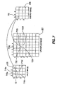
- the source pixel value 720 and the four closest neighbor pixel values 720a-720d in the upsampled image are shown in Fig. 7.
- Input image 205 and upsampled image 207 have a pixel value at each vertex formed by the horizontal and vertical lines shown in Fig 7.
- Pixel value 700 is a pixel value in warped image 200 which corresponds to source pixel 720. Pixel 700 also corresponds to pixel 710 in the input image.
- pixel values (720a, 720b, 720c and 720d) stored in the warp memory are retrieved at substantially the same time every clock cycle for use by the bilinear interpolator. These pixel values are then multiplied by the appropriate weights and summed to produce a pixel value in the intermediate warper image.
- the pixel values of the upsampled image signal 207 are stored in memories 600a-600d so that every grouping of the nearest pixel values 720a-720d to the source pixel value may be accessed concurrently.
- Write address generator 615 shown in Fig. 6, produces addresses for storing the pixel values in the upsampled image signal 207 in memories 600a-600d.
- Upsampler 10, shown in Fig. 1 produces a two-by-two array of pixel values [(A k,1 , E k,1 , F k,1 , G k,1 ,), (B k,1 , E k,1 , F k,1 , G k,1 ,), (C k,1 , E k,1 , F k,1 , G k,1 ,), or (D k,1 , E k,1 , F k,1 , G k,1 ,)] for each pixel value in the input image signal 205, shown in Fig.
- the four pixels in the two-by-two array are stored in separate memories 600a-600d at the same address in each memory 600a-600d and at substantially the same time. In the exemplary embodiment of the invention this is implemented by storing each of the output samples, OUT1, OUT2, OUT3 and OUT4 of the upsampler 10, shown in Fig. 3 in a respective memory 600a, 600b, 600c, and 600d.
- the upsampled image 207 shown in Fig. 7
- the upsampled image 207 has 512 pixel values by 512 pixel values where each square grouping of pixels 210, shown in Fig. 4, has a pixel located in a separate memory.
- the pixels values shown in Fig. 4 are stored in memories 600a-600d.
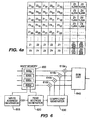
- Fig. 4a is a representation of the upsampled image signal 207 where the pixel values in the upsampled image signal 207, shown in Fig. 4, have been renumbered as Z1 through Z4 for describing where the pixel values in the upsampled image are stored in memories 600a-600d.
- Each memory address x p and y p is twelve bits if the maximum size is 2 12 X 2 12 (4096 X 4096).
- Each memory address x p and y p includes a least significant address bit x 0 and y 0 which together specify the memory 600a-600d in which the pixel value is stored and location address bits x 11-1 and y 11-1 which together specify the address at which the pixel values are stored.
- the mapping of address bits x 0 and y 0 into memories 600a-600d is shown in Table 1 below.
- Fig. 4a and Table 2 below illustrate the arrangement of the pixel values of the upsampled image 207 in memories 600a-600d addresses x[11-1] and y[11-1].
- x[11-1] y[11-1] MEMORY 600A MEMORY 600B MEMORY 600C MEMORY 600D 0 0 Z1 0,0 Z2 0,0 Z3 0,0 Z4 0,0 0 1 Z1 0,1 Z2 0,1 Z3 0,1 Z4 0,1 0 2 Z1 0,2 Z2 0,2 Z3 0,2 Z3 0,2 Z3 0,2 Z4 0,2 . . . . . . . . . . . . . . . .
- the upsampled image signal 207 may be warped by warper 20.
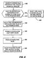
- the address value A[x,y] of the source pixel value 720 in the upsampled image is generated.
- x and y are coordinates of the source pixel value 720 in the upsampled image and are used as an address to memories 600a-600d described above with reference to Tables 1 and 2.
- address generator 620 generates an address value A[x,y] for the source pixel value 720 in the upsampled image 207, shown in Fig. 7.
- the input image 205 can be transformed in the spatial domain using a geometric transformation illustrated in equations (1) and (2) below.
- the transform equations are provided to the address generator 620 via control signal CS1 which is provided via an interface (not shown). Alternatively, the transform equations can be stored in a memory (not shown) in address generator 620.
- Equations (1) and (2) are implemented using the pseudo code in Table 3 below.
- x[u,v] is the x-coordinate of address value A[x,y] in the upsampled image 207 which corresponds to a pixel value in the intermediate warped image signal shown in Fig. 1.
- This intermediate signal corresponds to the warped image 208 prior to down sampling by down sampler 30 shown in Fig. 1.
- the y-coordinate y[u,v] is generated using the pseudo code in Table 3 except x[u,v] in Table 3 is replaced with y[u,v] and the "x" subscripts are replaced with "y” subscripts.
- the pseudo code in Table 3 can be implemented in hardware using two adders including four accumulator registers for each computation to produce values x[u,v] and y[u,v].
- the precision of the address generation is high, for example, 32 to 48 bits, depending on the system requirements and accuracy required for the generation of the warped image 208, shown in Fig. 7.
- the address value A[x,y] has an integer part S x and S y and a fractional part T x and T y because the address value A[x,y] identifies the location of the source pixel 720 in the upsampled image 207, shown in Fig. 7, with sub-pixel precision.
- S x and S y are the respective integer parts of the coordinate values x and y and T x and T y are the respective fractional parts of the coordinate values x and y.
- the integer part S x and S y of the address value A[x,y] is used to select the two-by-two pixel neighborhood of the source pixel value at address value A[x,y].
- the fractional part T x and T y of the address value A[x,y] is used to compute the interpolation coefficients that are provided to the bilinear interpolator.
- Interpolation coefficient values weight the pixel values in the two-by-two pixel neighborhood to produce the pixel value in the intermediate warped image shown in Fig. 1.
- step 810 after the address value A[x,y] has been generated, it is determined whether the source pixel 720 corresponds to one of the pixel values in the upsampled image signal 207. If so, the pixel value in the warped image is selected as the pixel value in the intermediate warped image signal. For example, if the address value A[x,y] identifies pixel value 720a, shown in Fig. 7, as the source pixel, then pixel value 720a is selected. Otherwise step 830 is performed.
- the two-by-two pixel neighborhood 720a-720d of the source pixel 720 is selected.
- the above-referenced article by Gomez describes one method for selecting and retrieving the two-by-two pixel neighborhood from four separate memories.
- source pixel 720 is located within a two-by-two neighborhood of pixels 720a-720d which are used to produce the pixel value in the intermediate warped image signal.
- the four pixels 720a-720d which make up the two-by-two neighborhood are located in separate memories 600a-600d.
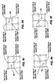
- Figure 9 is an enlarged view of a portion of the upsampled image 207 shown in Figure 7.
- Address generator 620 uses the upper left-most pixel as a nearest neighbor of the two-by-two neighborhood. The nearest neighbor is the starting position from which the address value for each pixel value 720a-720d in memories 600a-600d is determined.
- Figures 9(c)-9(f) illustrate the four different positions of source pixel 720 as it relates to pixel values 720a - 720d which form the two-by-two neighborhood.
- a pixel value of the upsampled image is located at each vertex created by the vertical and horizontal lines in Figures 9(c)-9(f).
- Figs. 9(c)-9(f) also show in which memory 600a-600d each pixel value 720a-720d of the two-by-two neighborhood is stored.
- the integer part S x and S y of the address value A[x,y] of the source pixel value 720 is used to determine the addresses of the two-by-two neighborhood in memories 600a-600d. Particularly, the least significant bit of the integer part S x [0] and S y [0] are used to determine the addresses.
- the address of each one of the pixel values 720a-720d in the two-by-two neighborhood is determined in accordance with Table 4 below.
- Memory X Component Address Y Component Address Memory 600a S x [11-1] S y [11-1] Memory 600b S x [11-1] S y [11-1] Memory 600c S x [11-1] S y [11-1] Memory 600d S x [11-1] S y [11-1]
- S x [11-1] are the eleven most significant bits of the x component part calculated using equation (1) and S y [11-1] are the eleven most significant bits of the y component part calculated in accordance with equation (2).
- the addresses of pixel values 720a-720d in memories 600a-600d are determined in accordance with Table 5 if the nearest neighbor to source pixel value 720 is stored in memory 600b.
- Memory X Component Address Y Component Address Memory 600a S x [11-1]+1 S y [11-1] Memory 600b S x [11-1] S y [11-1] Memory 600c S x [11-1]+1 S y [11-1] Memory 600d S x [11-1] S y [11-1]
- the addresses of pixel values 720a-720d in memories 600a-600d are determined in accordance with Table 6 if the nearest neighbor to source pixel value 720 is stored in memory 600c.
- Memory X Component Address Y Component Address Memory 600a S x [11-1] S y [11-1]+1 Memory 600b S x [11-1] S y [11-1]+1 Memory 600c S x [11-1] S y [11-1] Memory 600d S x [11-1] S y [11-1]
- the addresses of pixel values 720a-720d in memories 600a-600d are determined in accordance with Table 7 if the nearest neighbor to source pixel value 720 is stored in memory 600d.
- Memory X Component Address Y Component Address Memory 600a S x [11-1]+1 S y [11-1]+1 Memory 600b S x [11-1] S y [11-1]+1 Memory 600c S x [11-1]+1 S y [11-1] Memory 600d S x [11-1] S y [11-1]
- the pixel values 720a-720d are retrieved from memories 720a-720d.
- interpolation coefficient values I1, I2, I3, and I4 are produced using the fractional parts T x and T y of address value A[x,y].
- Interpolation coefficients I1, and I2, I3, and I4 are produced using equations (3)-(6) below.
- I1 (1-T x )•(1- T y )
- I2 T x •(1- T y )
- I3 (1-T x )•T y
- I4 T x •T y
- interpolation coefficient values I1-I4 can be stored in a look-up table in coefficient generator 630.
- the fractional parts T x and T y of the address value A[x,y] are used as an address to the interpolation coefficient values stored in the look-up table.
- the above-referenced paper by Gomez describes one method for using the fractional parts T x and T y of the address value A[x,y] as an address for retrieving interpolation coefficient values from a look-up table.
- the source pixel value 720 is produced using the interpolation coefficients I1-I4 and the two-by-two neighborhood of pixels 720a-720d, shown in Fig. 7, retrieved from memories 600a-600d.
- pixel value 720a from memory 600a and interpolation coefficient value I1 are multiplied at multiplier 610a.
- Pixel value 720b from memory 600b and interpolation coefficient value I2 are multiplied at multiplier 610b.
- Pixel value 720c from memory 600c and interpolation coefficient value I3 are multiplied at multiplier 610c.
- Pixel value 720d from memory 600d and interpolation coefficient value I4 are multiplied at multiplier 610d.
- the output values provided from multipliers 610a-610d are added together by sum circuitry 640 to produce source pixel 720, shown in Fig. 7.
- the source pixel 720 is selected as a pixel value in the intermediate warped image signal. Steps 800 through 860 are then repeated to produce each pixel in the warped image 208.
- Down sampler 30 reduces the number of samples in the intermediate warped image signal by the same factor the input image signal is upsampled. For example, if the input image signal is upsampled by two, then the intermediate warped image is down sampled by two.
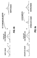
- Fig. 9(a) shows respective Fourier transforms of the upsampled image signal 207, the intermediate warped image, and the warped image 700 illustrating the operation of the down sampler 30.
- Fig. 9(b) shows Fourier transform of a input image signal using a bilinear interpolation which does not include upsampling the input image signal.
- a comparison of the warped image signals shown in Figs. 9(a) and 9(b) illustrates that the warped image signal produced using upsampling prior to transformation and down sampling after transformation produces a warped signal with better frequency characteristics than a warped signal which does not use upsampling and down sampling.
- the down sampler 30 and the warper 20 can be combined into a single component or step.
- the address value A[x,y] is adjusted by the interpolation factor 2 N to account for the interpolation of the input image signal 205.
- the same pixel value in the upsampled image signal 207 is accessed by multiplying the referenced address by 2.
- the neighborhood of pixel values in the upsampled image corresponds to sample points of the original analog image that are closer to the location of the source pixel than an equal sized neighborhood of pixel values in the input image signal.
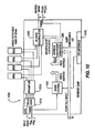
- Fig. 10 is an exemplary integrated circuit embodiment of the present invention directed to a warper chip 1000.
- Warper chip 1000 is provided with the input image signal which is a multi-bit digital signal containing at least eight data bits and two timing bits.
- the two timing bits convey respective timing signals.
- One signal, HA in is in a logic high state when the data in a line is valid (i.e. during the active line interval) and in a logic low state otherwise (i.e. during the horizontal blanking interval).
- the other signal, VA in is in a logic high state when the data in a field is valid and in a logic low state otherwise (i.e. during the vertical blanking interval).
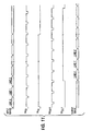
- Figure 11 is a timing diagram which illustrates the relative timing of the input image signal and the warped image signal, and the signals HA and VA for those signals.
- the warper chip uses the timing signals HA and VA in the same manner as described in U.S. Patent No. 5,359,674, entitled PYRAMID PROCESSOR INTEGRATED CIRCUIT, issued to van der Wal.
- the timing signals HA and VA remain associated with the input image signal as the input image signal is processed by the warper chip 1000.
- the warped image signal is produced, the vertical and horizontal blanking periods of the warped image signal do not need to be generated because the relative timing of the warped image signal is maintained by associating the timing signals HA and VA with the input image signal as it is processed.
- the upsampling and the storing process may be uncoupled from the warping and interpolation process, in which case the HA and VA timing signals for the output have to be regenerated. A further description of the use of the timing signals is omitted.
- the exemplary embodiment is not limited to processing multi-bit digital signals containing eight data bits and two timing bits.
- the exemplary embodiment can be configured to receive multi-bit digital signals containing, for example, ten data bits and two timing bits.
- the input image signal is provided to delay 1010 and upsampler 1015.
- Delay 1010 is the same as delay 200 shown in Fig. 2 and upsampler 1015 is the combination of vertical filter 210 and 220, shown in Fig. 2, and horizontal filters 230 and 240, shown in Fig. 2.
- Delay 1010 and upsampler 1015 operate the same as these components.
- Memories 600a-600d are the same as memories 600a-600d shown in Fig. 6 and are a single or double bank of SRAM.
- Bilinear interpolator is a combination of multipliers 610a-610d and sum circuitry 640 shown in Fig. 6.
- Address/coefficient generator 1050 operates the same as address generator 620 and coefficient generator 630 shown in Fig. 6 except that address/coefficient generator 1050 may also receive a flow field input.
- the flow field input provides a two-dimensional vector for each output pixel.
- the flow field vector is added to the warp address generated by the address/coefficient generator 1050 to allow completely general image transformations or to provide general modifications to the computed data of the address/coefficient and generator.
- Address/coefficient generator 1050 also receives control signals CS1 from CPU interface 1040.
- Warp coefficients such as constant coefficient values a x , b x , C x , d x , e x , f x , a y , b y , C y , d y , e y , and f y are provided to generate address values A[x,y].
- Address values A[x,y] are used to. retrieve pixel values from memories 600a-600d as described above with reference to write address generator 615 shown in Fig. 6.
- Write address generator 1020 is also coupled to CPU interface 1040 which provides data that specifies which segment of the input image is to be processed and stored in memories 600a-600d.
- Write control logic 1020 provides the write address shown in Tables 1 and 2 for writing the pixel values in the upsampled image to memories 600a-600d. Based on the timing signals HA in and VA in and the program interface which specifies which segment of the input image signal should be stored, the write control logic 1020 generates the addresses to store the pixel values in memories 600a-600d in the same manner as described above.
- the circuitry shown in Figs 1 and 10 may be used to perform multiple image plane warping.
- multiple image planes such as the separate planes of a color image.
- This can be achieved by using multiple warper chips 1000, shown in Fig. 10, or multiple warper systems 5, shown in Fig. 1, in parallel.
- the processing rate of the warper chip 1000 or warping system 5 is fast enough, the warping operations on part or all the image planes can be interleaved. As a result, a single warper chip 1000 or warper system 5 can be used.
- the input image signal includes, for example, three image planes R, G, and B, where the image planes R, G, and B are interleaved for every pixel for each line of the input image signal as shown in Table 8 below.
- upsampler 1015 can operate on the input image signal in an interleaved fashion.
- the upsampled image is stored in memories 600a-600d in the same manner as described above except that the pixel values are stored in an interleaved fashion.
- Table 9 illustrates how the pixel values of the three planes are stored in memories 600a-600d.
- (o) represents the odd horizontal and vertical outputs of upsampler 1015.
- the integer part of the address value A[x,y] generated by address/coefficient generator 1050 is multiplied by three to account for the change in address created by the addition of the other image planes in memories.
- address/coefficient generator 1050 repeats the same operation three times: once for the calculated address value A[x,y], then for the address value A[x,y] incremented by one, and then for the address value A[x,y] incremented by two.
- the warped image signal includes color image data in an interleaved fashion.
- the warper chip operates at three times the clock rate of the incoming pixel rate of a single image plane. If the RGB image planes in the input image signal are only available in parallel data paths, the image data is interleaved prior to processing. After the warper image signal is produced, the warped image signal is de-interleaved to restore the image planes to parallel data paths.
- the input image signal is an color image in D1 format, where the three image data planes are interleaved in a slightly different manner.
- the input image signal includes, for example, three image planes Y, U, and V, where the image planes Y, U, and V are interleaved as ...U[n,m], Y[n,m], V[n,m], Y[n+1,m], U[n+2,m], Y[n+2,m], V[n+2,m], Y[n+3,m]...
- the luminance plane Y has twice the resolution of the two color planes U and V, and the color planes U and V are co-located with the even positions of the luminance plane Y.
- the line delays 1010 prior to the upsampler 1015 are twice the size of a line of the luminance plane Y which is four times the size of one line of the color planes U and V.
- the delay switches every clock cycle between a two-delay element and a four-delay element.
- the address/coefficient generator computes a new address value A[x,y] twice for four successive output values: first for the two color planes U and V and the even position of the luminance plane Y, and then an address value A[x,y] is separately calculated for the odd position of the luminance plane Y.
- the address value A[x,y] is also offset to appropriately access the correct data planes stored in memories 600a-600d.
Landscapes
- Physics & Mathematics (AREA)
- General Physics & Mathematics (AREA)
- Engineering & Computer Science (AREA)
- Theoretical Computer Science (AREA)
- Image Processing (AREA)
- Editing Of Facsimile Originals (AREA)
- Studio Circuits (AREA)
Claims (20)
- Bildverarbeitungssystem, das aufweist:eine Einrichtung für das Anlegen eines Eingangsbildsignals an das Bildverarbeitungssystem,eine Upsampling- (höhere Abtastrate) Einrichtung (10) für das Upsamplen des Eingangsbildsignals, um Eingangsbildsignalabfragen zu erzeugen, die gleichförmig mit einer Samplerate gesamplet sind, die um einen vorbestimmten Faktor von größer oder gleich zwei größer als die Nyquist-Rate ist, um ein upgesampletes Bildsignal zu erzeugen, undeine Einrichtung für das Warping bzw. Verzerren (20) des upgesampleten Bildsignals undfür das Downsampling (30) des upgesampleten verzerrten Bildsignals um den besagten Faktor, um ein verzerrtes Bildausgangssignal zu erzeugen.
- System nach Anspruch 1, wobeidie Anlegeeinrichtung derart angeordnet ist, daß sie ein gesampletes Eingangsbildsignal an das System anlegt, wobei das gesamplete Eingangsbildsignal eine Eingangssamplingrate hat, unddie Upsamplingeinrichtung (10) derart angeordnet ist, daß sie gleichförmig upgesamplete und interpolierte Abfragen erzeugt, wobei die Samplingrate auf eine Rate erhöht ist, die um den besagten Faktor größer als die Nyquist-Rate ist.
- System nach Anspruch 1 oder 2, wobei die Einrichtung für das Warping und das Downsampling aufweist:eine Einrichtung für das Warping (10) des gleichförmig gesampleten Signals, das von der Upsamplingeinrichtung erzeugt wird undeine Einrichtung für das Downsampling (30) des upgesampleten verzerrten Bildsignals um den besagten Faktor.
- System nach Anspruch 1 oder 2, wobei die Einrichtung für das Warping und Downsampling (10, 30), derart angeordnet ist, daß das upgesamplete Bildsignal in einem einzigen Schritt verzerrt und downgesamplet wird.
- System nach Anspruch 3 oder 4, wobei die Einrichtung für das Warping einen Interpolationsfilter beinhaltet, der eine Mehrzahl von benachbarten Abfragen des gleichförmig upgesampleten Bildes interpoliert, um jede Abfrage des upgesampleten verzerrten Bildes zu erzeugen.
- Bildverarbeitungssystem nach einem der Ansprüche 1, 2, 3, 4 oder 5, wobei die Warpingeinrichtung (10) einen Tiefpaßfilter beinhaltet und der Tiefpaßfilter einen bilinearen Interpolator (610, 640) aufweist.
- Bildverarbeitungssystem nach einem der Ansprüche 1, 2, 3, 4, 5 oder 6, wobei die Upsamplingeinrichtung (10) einen Filter (210-240) beinhaltet, der derart angeordnet ist, daß er das upgesamplete Bildsignal vorverarbeitet, um der Verschlechterung in der örtlichen Frequenzcharakteristik des upgesampleten verzerrten Bildsignals, die durch die Warpingeinrichtung verursacht wird, entgegenzuwirken.
- Bildverarbeitungssystem nach einem der Ansprüche 1, 2, 3, 4, 5, 6 oder 7, wobei:die Warpingeinrichtung vier Speicher (600) beinhaltet unddie Upsamplingeinrichtung (10) weiterhin vier Abfragen für jede der Abfragen des Ausgangsbildsignals erzeugt und die vier Abfragen jeweils in unterschiedlichen Speichern der vier Speicher (600) ablegt.
- System nach einem der Ansprüche 1 bis 8, wobei die Warpingeinrichtung (10) derart angeordnet ist, daß sie das verzerrte Bildsignal durch inverses Mapping bzw. inverse Abbildung erzeugt.
- Integrierter Schaltkreis, der aufweist:einen Eingangsanschluß für das Empfangen eines gesampleten Eingangsbildsignals mit einer Eingangssamplingrate,eine Upsamplingeinrichtung (1015), die mit dem Eingangsterminal verbunden ist für das Upsamplen des Eingangsbildsignals, um eine gleichförmig upgesamplete und interpolierte Eingangsbildsignalabfrage zu erzeugen, wobei die Samplingrate um einen Faktor größer oder gleich zwei größer als die Nyquist-Rate ist, um ein upgesampletes Bildsignal zu erzeugen,eine Adreßschreibeeinrichtung (1020) für das Erzeugen eines Schreibadreßsignals, das einen Ort in einem Speicher (600) spezifiziert, wo die upgesampleten Bildsignalabfragen gespeichert werden sollen,eine Leseadreßeinrichtung (1050) für das Erzeugen eines Leseadreßsignals, das spezifiziert, welche der abgelegten Abfragen von dem Speicher (600) abgefragt werden sollen, undeine Einrichtung (1030) für das Empfangen der abgerufenen Abfragen von dem Speicher und für das Erzeugen eines upgesampleten verzerrten Bildsignals und für das Downsampling des upgesampleten verzerrten Bildsignals um den besagten Faktor, um ein verzerrtes Bildausgangssignal zu erzeugen.
- Integrierter Schaltkreis nach Anspruch 10, wobei die Einrichtung für das Erzeugen eines upgesampleten verzerrten Bildsignals einen Interpolationsfilter beinhaltet, der eine Mehrzahl von benachbarten Abfragen des gleichförmig upgesampleten Bildes interpoliert, um jede Abfrage des upgesampleten verzerrten Bildes zu erzeugen.
- Integrierter Schaltkreis nach Anspruch 10 oder 11, wobei die Einrichtung für das Erzeugen eines verzerrten Bildsignals einen bilinearen Interpolator beinhaltet.
- Schaltkreis nach Anspruch 10, 11 oder 12, wobei die Einrichtung für das Erzeugen eines verzerrten Bildsignals und für das Downsamplen (10, 30) derart angeordnet ist, daß das upgesamplete Bildsignal in einem einzigen Schritt verzerrt und downgesampelt wird.
- Schaltkreis nach Anspruch 10, 11, 12 oder 13, wobei die Einrichtung (1030) für das Erzeugen eines verzerrten Bildsignals derart angeordnet ist, daß das verzerrte Bildsignal durch inverses Mapping bzw. inverses Abbilden erzeugt wird.
- Verfahren zum Verarbeiten eines Eingangsbildsignals, das die Schritte aufweist:Anlegen eines Eingangsbildsignals an das Bildverarbeitungssystem,Samplen des Eingangsbildsignals, um Eingangsbildsignalabfragen zu erzeugen, die gleichförmig mit einer Samplingrate gesamplet sind, die um einen vorbestimmten Faktor größer oder gleich zwei größer als die Nyquist-Rate ist, um ein upgesampletes Bildsignal zu erzeugen,Warping bzw. Verzerren (20) des upgesampleten Bildsignals undDownsamplen (30) des upgesampleten verzerrten Bildsignals um den besagten Faktor, um ein verzerrtes Bildausgangssignal zu erzeugen.
- Verfahren nach Anspruch 15, wobei der Schritt des Anlegens so angeordnet ist, daß ein gesampletes Eingangsbildsignal an das System angelegt wird, wobei das gesamplete Eingangsbildsignal eine Eingangssamplingrate hat, undder Upsamplingschritt (10) derart eingerichtet ist, daß er gleichförmig upgesamplete und interpolierte Abfragen erzeugt, wobei die Abfragerate bzw. Samplingrate auf eine Rate, die um den besagten Faktor größer als die Nyquist-Rate ist, angehoben ist.
- Verfahren nach Anspruch 16, wobei der Schritt des Verzerrens das Interpolieren einer Mehrzahl von benachbarten Abfragen des gleichförmig untergesampleten Bildes aufweist, um jede Abfrage des upgesampleten verzerrten Bildes zu erzeugen.
- Verfahren nach Anspruch 15, 16 oder 17, wobei der Warpingschritt das inverse Mapping bzw. das inverse Abbilden verwendet.
- Verfahren nach Anspruch 15, 16, 17 oder 18, wobei der Upsamplingschritt das Zurverfügungstellen von Bildsignalabfragen mit einer Rate von 2N-mal der Nyquist-Rate aufweist, wobei N eine positive ganze Zahl größer oder gleich eins ist.
- Verfahren nach Anspruch 15, 16, 17, 18 oder 19, wobeider Upsamplingschritt vier Pixelwerte in dem upgesampleten Bildsignal für jede der Abfragen des Ausgangssignals erzeugt unddas Verfahren weiterhin den Schritt aufweist des Ablegens jedes der vier Pixelwerte in einem getrennten Speicher (600).
Applications Claiming Priority (3)
| Application Number | Priority Date | Filing Date | Title |
|---|---|---|---|
| US1557796P | 1996-04-18 | 1996-04-18 | |
| US15577P | 1996-04-18 | ||
| PCT/US1997/005427 WO1997039420A1 (en) | 1996-04-18 | 1997-04-17 | Computationally efficient digital image warping |
Publications (3)
| Publication Number | Publication Date |
|---|---|
| EP0920671A1 EP0920671A1 (de) | 1999-06-09 |
| EP0920671A4 EP0920671A4 (de) | 2001-09-19 |
| EP0920671B1 true EP0920671B1 (de) | 2003-07-09 |
Family
ID=21772243
Family Applications (1)
| Application Number | Title | Priority Date | Filing Date |
|---|---|---|---|
| EP97920043A Expired - Lifetime EP0920671B1 (de) | 1996-04-18 | 1997-04-17 | Deformation eines digitalen bildes mit effizienter berechnung |
Country Status (5)
| Country | Link |
|---|---|
| US (1) | US6061477A (de) |
| EP (1) | EP0920671B1 (de) |
| JP (1) | JP2000511715A (de) |
| DE (1) | DE69723451T2 (de) |
| WO (1) | WO1997039420A1 (de) |
Cited By (3)
| Publication number | Priority date | Publication date | Assignee | Title |
|---|---|---|---|---|
| US7064770B2 (en) | 2004-09-09 | 2006-06-20 | Silicon Optix Inc. | Single-pass image resampling system and method with anisotropic filtering |
| US8055070B2 (en) | 2007-01-05 | 2011-11-08 | Geo Semiconductor Inc. | Color and geometry distortion correction system and method |
| US8442316B2 (en) | 2007-01-05 | 2013-05-14 | Geo Semiconductor Inc. | System and method for improving color and brightness uniformity of backlit LCD displays |
Families Citing this family (34)
| Publication number | Priority date | Publication date | Assignee | Title |
|---|---|---|---|---|
| US5845015A (en) | 1995-10-12 | 1998-12-01 | Sarnoff Corporation | Method and apparatus for resizing images using the discrete cosine transform |
| US6281931B1 (en) * | 1997-11-04 | 2001-08-28 | Tien Ren Tsao | Method and apparatus for determining and correcting geometric distortions in electronic imaging systems |
| US6211913B1 (en) | 1998-03-23 | 2001-04-03 | Sarnoff Corporation | Apparatus and method for removing blank areas from real-time stabilized images by inserting background information |
| US6538691B1 (en) * | 1999-01-21 | 2003-03-25 | Intel Corporation | Software correction of image distortion in digital cameras |
| US6178272B1 (en) * | 1999-02-02 | 2001-01-23 | Oplus Technologies Ltd. | Non-linear and linear method of scale-up or scale-down image resolution conversion |
| JP4392082B2 (ja) * | 1999-08-06 | 2009-12-24 | ヒューレット・パッカード・カンパニー | 彫版風ハーフトーン画像生成方法・装置 |
| KR100311482B1 (ko) * | 1999-10-21 | 2001-10-18 | 구자홍 | 보간 영상의 화질 개선을 위한 필터링 제어방법 |
| US6906732B1 (en) * | 1999-12-07 | 2005-06-14 | Nintendo Co., Ltd. | Texture morphing process provided by the preferred embodiment of the present invention |
| GB2360919A (en) * | 2000-01-20 | 2001-10-03 | Anthropics Technology Ltd | Appearance modelling |
| US6738498B1 (en) * | 2000-08-01 | 2004-05-18 | Ge Medical Systems Global Technology Company, Llc | Method and apparatus for tissue dependent filtering for image magnification |
| EP1354292B1 (de) * | 2000-12-01 | 2012-04-04 | Imax Corporation | Verfahren und Vorrichtung zum Erzeugen hochauflösender Bilder |
| JP2002224982A (ja) * | 2000-12-01 | 2002-08-13 | Yaskawa Electric Corp | 薄型基板搬送用ロボットおよび薄型基板検出方法 |
| AU2002216240A1 (en) * | 2000-12-22 | 2002-07-08 | Anthropics Technology Limited | Communication system |
| EP1518211A2 (de) * | 2000-12-22 | 2005-03-30 | Anthropics Technology Limited | Bildbearbeitungssystem |
| US6756993B2 (en) * | 2001-01-17 | 2004-06-29 | The University Of North Carolina At Chapel Hill | Methods and apparatus for rendering images using 3D warping techniques |
| CA2360295A1 (en) * | 2001-10-26 | 2003-04-26 | Jaldi Semiconductor Corp. | System and method for image warping |
| CN1650622B (zh) * | 2002-03-13 | 2012-09-05 | 图象公司 | 用于数字重新灌录或修改电影或其他图像序列数据的系统和方法 |
| JP3979894B2 (ja) * | 2002-07-22 | 2007-09-19 | 本田技研工業株式会社 | 物体検出装置及び方法 |
| WO2004079901A2 (en) * | 2003-03-04 | 2004-09-16 | Oticon A/S | Digital filter and listening device |
| KR100519776B1 (ko) * | 2003-11-24 | 2005-10-07 | 삼성전자주식회사 | 영상 신호의 해상도 변환 방법 및 장치 |
| US7590306B2 (en) * | 2003-11-26 | 2009-09-15 | Ge Medical Systems Global Technology Company, Llc | Resolution adaptive image filtering system and method |
| US7460730B2 (en) | 2005-08-04 | 2008-12-02 | Microsoft Corporation | Video registration and image sequence stitching |
| US7606445B2 (en) * | 2005-11-30 | 2009-10-20 | General Electric Company | Methods and systems for ultrasound inspection |
| US8842730B2 (en) * | 2006-01-27 | 2014-09-23 | Imax Corporation | Methods and systems for digitally re-mastering of 2D and 3D motion pictures for exhibition with enhanced visual quality |
| CN102685533B (zh) * | 2006-06-23 | 2015-03-18 | 图象公司 | 对2d电影进行转换用于立体3d显示的方法和系统 |
| US20080088527A1 (en) * | 2006-10-17 | 2008-04-17 | Keitaro Fujimori | Heads Up Display System |
| US20080088528A1 (en) * | 2006-10-17 | 2008-04-17 | Takashi Shindo | Warp Image Circuit |
| US8121434B2 (en) | 2008-06-13 | 2012-02-21 | Microsoft Corporation | Multi-pass image resampling |
| US8675994B1 (en) * | 2010-06-17 | 2014-03-18 | Ambarella, Inc. | High performance warp correction in two-dimensional images |
| US10616578B2 (en) * | 2015-01-30 | 2020-04-07 | Texas Instruments Incorporated | Semi-global matching (SGM) cost compression |
| US11178072B2 (en) | 2015-06-10 | 2021-11-16 | Mobileye Vision Technologies Ltd. | Image processor and methods for processing an image |
| EP3308349B1 (de) * | 2015-06-10 | 2025-01-29 | Mobileye Vision Technologies Ltd. | Bildprozessor und verfahren zur verarbeitung eines bildes |
| KR102674906B1 (ko) * | 2017-06-27 | 2024-06-12 | 가부시키가이샤 한도오따이 에네루기 켄큐쇼 | 표시 시스템 및 데이터 처리 방법 |
| CN114497170A (zh) | 2017-08-25 | 2022-05-13 | 株式会社半导体能源研究所 | 显示面板及显示装置 |
Family Cites Families (13)
| Publication number | Priority date | Publication date | Assignee | Title |
|---|---|---|---|---|
| US3700815A (en) * | 1971-04-20 | 1972-10-24 | Bell Telephone Labor Inc | Automatic speaker verification by non-linear time alignment of acoustic parameters |
| US4816913A (en) * | 1987-11-16 | 1989-03-28 | Technology, Inc., 64 | Pixel interpolation circuitry as for a video signal processor |
| US5008752A (en) * | 1989-06-16 | 1991-04-16 | Eastman Kodak Company | Digital image interpolator with multiple interpolation algorithms |
| US5204944A (en) * | 1989-07-28 | 1993-04-20 | The Trustees Of Columbia University In The City Of New York | Separable image warping methods and systems using spatial lookup tables |
| US5175808A (en) * | 1989-09-12 | 1992-12-29 | Pixar | Method and apparatus for non-affine image warping |
| EP0427436B1 (de) * | 1989-11-09 | 1996-12-27 | Ikegami Tsushinki Co., Ltd. | Bildeinstellungs- und Konturkorrekturschaltung und Verfahren für Festkörperkamera |
| US5173948A (en) * | 1991-03-29 | 1992-12-22 | The Grass Valley Group, Inc. | Video image mapping system |
| US5355328A (en) * | 1991-09-27 | 1994-10-11 | Northshore Laboratories, Inc. | Resampling apparatus suitable for resizing a video image |
| US5410616A (en) * | 1992-05-28 | 1995-04-25 | Unisys Corporation | Loop-up table image scaling for rational factors |
| US5420940A (en) * | 1992-06-16 | 1995-05-30 | Hughes Training, Inc. | CGSI pipeline performance improvement |
| US5642167A (en) * | 1992-07-23 | 1997-06-24 | Wallace; Richard Scot | TV picture compression and expansion |
| CA2129092C (en) * | 1993-10-04 | 1999-10-19 | Leon C. Williams | Image interpolation apparatus |
| US5594676A (en) * | 1994-12-22 | 1997-01-14 | Genesis Microchip Inc. | Digital image warping system |
-
1997
- 1997-04-15 US US08/838,101 patent/US6061477A/en not_active Expired - Lifetime
- 1997-04-17 DE DE69723451T patent/DE69723451T2/de not_active Expired - Fee Related
- 1997-04-17 EP EP97920043A patent/EP0920671B1/de not_active Expired - Lifetime
- 1997-04-17 JP JP09537130A patent/JP2000511715A/ja not_active Ceased
- 1997-04-17 WO PCT/US1997/005427 patent/WO1997039420A1/en not_active Ceased
Cited By (3)
| Publication number | Priority date | Publication date | Assignee | Title |
|---|---|---|---|---|
| US7064770B2 (en) | 2004-09-09 | 2006-06-20 | Silicon Optix Inc. | Single-pass image resampling system and method with anisotropic filtering |
| US8055070B2 (en) | 2007-01-05 | 2011-11-08 | Geo Semiconductor Inc. | Color and geometry distortion correction system and method |
| US8442316B2 (en) | 2007-01-05 | 2013-05-14 | Geo Semiconductor Inc. | System and method for improving color and brightness uniformity of backlit LCD displays |
Also Published As
| Publication number | Publication date |
|---|---|
| DE69723451T2 (de) | 2004-04-15 |
| JP2000511715A (ja) | 2000-09-05 |
| EP0920671A4 (de) | 2001-09-19 |
| WO1997039420A1 (en) | 1997-10-23 |
| US6061477A (en) | 2000-05-09 |
| EP0920671A1 (de) | 1999-06-09 |
| DE69723451D1 (de) | 2003-08-14 |
Similar Documents
| Publication | Publication Date | Title |
|---|---|---|
| US6061477A (en) | Quality image warper | |
| EP0800687B1 (de) | Digitales videoumwandlungsschaltsystem | |
| JP3762446B2 (ja) | 高速画像サイズ変更に応用するディジタル再標本化集積回路 | |
| JP3266273B2 (ja) | 離散コサイン変換を用いて画像をリサイズする方法および装置 | |
| US7254281B2 (en) | Method and apparatus for electronic image processing | |
| EP1041511B1 (de) | System und Verfahren zur massstäblichen Umformung von Bildern | |
| US5202670A (en) | Image processing apparatus | |
| US5410616A (en) | Loop-up table image scaling for rational factors | |
| US4908874A (en) | System for spatially transforming images | |
| JP3190762B2 (ja) | デジタルビデオ特殊効果装置 | |
| JPH05504433A (ja) | 画像のサイズを変換する方法、フィルタを設計する方法および出力画像空間のピクセルをサイズ変換された入力画像空間に写像する方法 | |
| US5930407A (en) | System and method for efficiently generating cubic coefficients in a computer graphics system | |
| JP4191246B2 (ja) | 映像フィールドを順次走査映像フレームへ非飛び越し走査するための方法および装置 | |
| US5438654A (en) | System and method for sharpening texture imagery in computer generated interactive graphics | |
| US7660486B2 (en) | Method and apparatus of removing opaque area as rescaling an image | |
| US5440653A (en) | Image mirroring and image extension for digital filtering | |
| AU2007219336B2 (en) | Method and apparatus for abitrary ratio image reduction | |
| US5483474A (en) | D-dimensional, fractional bandwidth signal processing apparatus | |
| JPH08251400A (ja) | 複数の補間カーネルを備えたデジタル画像補間回路 | |
| EP0511606B1 (de) | Parallelinterpolator für Hochgeschwindigkeits-Digitalbildvergrösserung | |
| EP1474777A2 (de) | Stufenlose 3-d-texturabbildung in rechnergraphik | |
| US5506693A (en) | Addressing mechanism for interfacing spatially defined imagery data with sequential memory | |
| CN1053548C (zh) | 视频信号变换装置及其中使用的噪声抑制器 | |
| JPH04500747A (ja) | デジタル映像効果の形成ならびにそれに関連する改良 | |
| JP3698926B2 (ja) | 映像特殊効果装置 |
Legal Events
| Date | Code | Title | Description |
|---|---|---|---|
| PUAI | Public reference made under article 153(3) epc to a published international application that has entered the european phase |
Free format text: ORIGINAL CODE: 0009012 |
|
| 17P | Request for examination filed |
Effective date: 19981109 |
|
| AK | Designated contracting states |
Kind code of ref document: A1 Designated state(s): DE FR GB IT NL |
|
| A4 | Supplementary search report drawn up and despatched |
Effective date: 20010806 |
|
| AK | Designated contracting states |
Kind code of ref document: A4 Designated state(s): DE FR GB IT NL |
|
| 17Q | First examination report despatched |
Effective date: 20011127 |
|
| GRAH | Despatch of communication of intention to grant a patent |
Free format text: ORIGINAL CODE: EPIDOS IGRA |
|
| RIC1 | Information provided on ipc code assigned before grant |
Free format text: 7G 06T 3/00 A |
|
| GRAH | Despatch of communication of intention to grant a patent |
Free format text: ORIGINAL CODE: EPIDOS IGRA |
|
| GRAA | (expected) grant |
Free format text: ORIGINAL CODE: 0009210 |
|
| AK | Designated contracting states |
Designated state(s): DE FR GB IT NL |
|
| REG | Reference to a national code |
Ref country code: GB Ref legal event code: FG4D |
|
| REF | Corresponds to: |
Ref document number: 69723451 Country of ref document: DE Date of ref document: 20030814 Kind code of ref document: P |
|
| ET | Fr: translation filed | ||
| PLBE | No opposition filed within time limit |
Free format text: ORIGINAL CODE: 0009261 |
|
| STAA | Information on the status of an ep patent application or granted ep patent |
Free format text: STATUS: NO OPPOSITION FILED WITHIN TIME LIMIT |
|
| 26N | No opposition filed |
Effective date: 20040414 |
|
| PG25 | Lapsed in a contracting state [announced via postgrant information from national office to epo] |
Ref country code: NL Free format text: LAPSE BECAUSE OF NON-PAYMENT OF DUE FEES Effective date: 20041101 |
|
| NLV4 | Nl: lapsed or anulled due to non-payment of the annual fee |
Effective date: 20041101 |
|
| PGFP | Annual fee paid to national office [announced via postgrant information from national office to epo] |
Ref country code: FR Payment date: 20060417 Year of fee payment: 10 |
|
| PGFP | Annual fee paid to national office [announced via postgrant information from national office to epo] |
Ref country code: GB Payment date: 20060424 Year of fee payment: 10 |
|
| PGFP | Annual fee paid to national office [announced via postgrant information from national office to epo] |
Ref country code: DE Payment date: 20060531 Year of fee payment: 10 |
|
| GBPC | Gb: european patent ceased through non-payment of renewal fee |
Effective date: 20070417 |
|
| PG25 | Lapsed in a contracting state [announced via postgrant information from national office to epo] |
Ref country code: DE Free format text: LAPSE BECAUSE OF NON-PAYMENT OF DUE FEES Effective date: 20071101 |
|
| PG25 | Lapsed in a contracting state [announced via postgrant information from national office to epo] |
Ref country code: GB Free format text: LAPSE BECAUSE OF NON-PAYMENT OF DUE FEES Effective date: 20070417 |
|
| PG25 | Lapsed in a contracting state [announced via postgrant information from national office to epo] |
Ref country code: FR Free format text: LAPSE BECAUSE OF NON-PAYMENT OF DUE FEES Effective date: 20070430 |
|
| PGFP | Annual fee paid to national office [announced via postgrant information from national office to epo] |
Ref country code: IT Payment date: 20090428 Year of fee payment: 13 |
|
| PG25 | Lapsed in a contracting state [announced via postgrant information from national office to epo] |
Ref country code: IT Free format text: LAPSE BECAUSE OF NON-PAYMENT OF DUE FEES Effective date: 20100417 |